






Introduction
Practical millimeter-wave (mm-Waves) and terahertz (THz) systems require integration platforms that combine low-loss guiding, compactness, and robust packaging. Although conventional hollow metallic waveguides remain prevalent in laboratory settings, their performance at THz frequencies is constrained by Drude loss, tight fabrication tolerances, and mechanically fragile packaging factors that hinder large-scale integration and mass manufacturing [Reference Siegel1–Reference Headland, Monnai, Abbott, Fumeaux and Withayachumnankul3]. These limitations have motivated an extensive shift toward all-dielectric THz waveguides, particularly those based on high-resistivity intrinsic silicon, which offers near-lossless propagation, strong field confinement, and compatibility with mature microfabrication processes [Reference Mendis and Grischkowsky4–Reference Jianqiang, Shrestha, Adelberg, Yeh, Hossain, Knightly, Jornet and Mittleman6]. In this context, substrateless all-silicon (Si) microstructures have emerged as a promising THz integration platform, enabling low-loss guiding, monolithic integration of diverse components, and simplified packaging within a mechanically robust frame [Reference Headland, Fujita, Carpintero, Nagatsuma and Withayachumnankul7–Reference Headland, Withayachumnankul, Xiongbin, Fujita and Nagatsuma9].
Efficient low-loss THz interconnects have been reported and could be prime candidates for meeting the ever-growing demand for higher data rates in short-range interconnection applications [Reference Nagatsuma, Ducournau and Renaud10, Reference Song and Nagatsuma11]. THz interconnects bridge the gap between board-level links and the limited bandwidth of electrical chip-to-chip connections. These short-range links, typically spanning a few centimeters, are commonly referred to as “last-centimeter interconnects” [Reference Song and Nagatsuma11, Reference Yu, Liu, Ye, Liu and Qun Jane12]. Si dielectric THz waveguides have already demonstrated applications toward 6G and beyond, with propagation loss below 0.05 dB/cm and bandwidths on the order of  ${\sim}{350}\,{GHz}$ [Reference Gao, Xiongbin, Fujita, Nagatsuma, Fumeaux and Withayachumnankul13, Reference Ratmalgre, Fujita and Nagatsuma14]. Representative all-Si THz waveguide platforms include photonic crystal waveguides, effective-medium (EM) waveguides, and unclad dielectric wire waveguides [Reference Headland, Fujita, Carpintero, Nagatsuma and Withayachumnankul7–Reference Headland, Withayachumnankul, Xiongbin, Fujita and Nagatsuma9]. For comparison, conventional metallic rectangular waveguides in the same frequency range typically exhibit attenuation on the order of 0.5–2 dB/cm, depending on band and surface finish, as can be inferred from standard manufacturer data and attenuation charts for WR-series waveguides. This illustrates that silicon dielectric rectangular waveguides can achieve more than an order of magnitude reduction in propagation loss compared with conventional hollow metallic waveguides, while also offering improved integration and packaging flexibility.
Photonic crystal waveguides can achieve very low loss ( ${ \lt }{0.1}\,{dB/cm}$), but their operation bandwidth is typically limited to
 ${\sim}{20}\,{GHz}$ due to the inherent constraints of photonic band gap guiding [Reference Ishigaki, Fujita, Nagai, Ashida and Nagatsuma15, Reference Yata, Fujita and Nagatsuma16]. EM waveguides retain similarly low loss while offering significantly wider bandwidths reported values reach
 ${\sim}{120}\,{GHz}$ around 0.3 THz and
 ${\sim}{350}\,{GHz}$ in the 1 THz band [Reference Gao, Xiongbin, Fujita, Nagatsuma, Fumeaux and Withayachumnankul13, Reference Ratmalgre, Fujita and Nagatsuma14]. However, EM waveguide designs rely on intricate subwavelength perforations that demand high-precision etching, which complicates scaling and limits design flexibility. Unclad all-silicon waveguides have been proposed to relax some of these constraints, they can preserve propagation losses below 0.1 dB/cm with bandwidths comparable to effective-medium platforms [Reference Headland, Withayachumnankul, Xiongbin, Fujita and Nagatsuma9, Reference Headland and Carpintero17], while simplifying the microstructure and enabling more straightforward implementation of bends, splitters, and couplers [Reference Headland, Gallego, Sakaki, Benson and Carpintero18, Reference Gao, Fujita, Murakami, Nagatsuma, Fumeaux and Withayachumnankul19]. Collectively, these all-silicon waveguide platforms now provide versatile components for low-loss THz interconnects and functional integrated components [Reference Headland, Fujita, Carpintero, Nagatsuma and Withayachumnankul7, Reference Ratmalgre, Fujita and Nagatsuma8].
Despite these advances, dielectric waveguides alone do not intrinsically offer the mechanical flexibility required for chip-to-chip or board-to-board interconnections, since they are typically fabricated from high-resistivity crystalline Si with limited bendability. To address this, hollow-core fibers have attracted considerable attention as flexible THz interconnects [Reference Bowden, Harrington and Mitrofanov20, Reference Lai, Hsueh, Chen, Huang, Chang and Sun21]. More recently, flexible Polytetrafluoroethylene (PTFE)-core solid dielectric waveguides have been explored for mm-Waves applications [Reference Hao, Zhang and Zhu22]. In that work, PTFE circular dielectric waveguides with diameters of 0.5 and 1 mm were designed and characterized across the 325–500 GHz band, demonstrating measured transmission losses below 0.3 and 0.33 dB/cm, respectively, and bending losses below 0.01 dB/cm [Reference Hao, Zhang and Zhu22]. However, coupling from metallic waveguides via horn-based launchers introduced approximately  $3\,\mathrm{dB}$ of insertion loss, and segment-to-segment interconnection using PTFE heat shrink tubes added a further 1.6–2.5 dB [Reference Hao, Zhang and Zhu22]. Despite their mechanical flexibility, these waveguides are therefore less suitable for low-loss, high-performance THz interconnects.
A notable step forward is the recently demonstrated THz fiber link using a dielectric silicon waveguide interface [Reference Koala, Iyoda, Gao, Matsuura, Fujita and Nagatsuma23]. In this work, a tapered all-Si dielectric waveguide is employed as an efficient coupler between a THz hollow core fiber and a silicon dielectric waveguide, enabling a 22 Gbit/s link in the 0.3 THz band with a coupling efficiency of  ${\sim}60\%$ and a
 $3\,\mathrm{dB}$ bandwidth of
 $150\,\mathrm{GHz}$ over 10 cm of fiber [Reference Koala, Iyoda, Gao, Matsuura, Fujita and Nagatsuma23]. This result highlights that carefully engineered dielectric couplers can substantially improve interface efficiency and throughput, underscoring the potential of THz interconnects as practical “last-centimeter” links for high-speed, short-range communications. At the same time, it also exemplifies a broader trend in THz integration: most high-performance dielectric interconnects to date still rely on relatively long, carefully shaped tapers or complex couplers whose performance can be sensitive to fabrication tolerances and mechanical misalignment [Reference Headland, Withayachumnankul, Xiongbin, Fujita and Nagatsuma9, Reference Headland and Carpintero17, Reference Amarloo and Safavi-Naeini24]. This motivates compact waveguide-to-waveguide interconnect schemes on substrateless all-Si platforms that preserve low loss and wide bandwidth while improving robustness to misalignment at module-to-module interfaces. From the perspective of practical mm-Waves and THz hybrid integration, the most relevant figures of merit for dielectric waveguide-to-waveguide interconnect schemes are not limited to insertion loss alone, but also include operational bandwidth, interface compactness, and robustness to assembly tolerances. Existing taper-based or fiber-coupled dielectric interfaces can provide efficient coupling, but they often rely on comparatively long transition regions or mechanically demanding alignment conditions [Reference Hao, Zhang and Zhu22, Reference Koala, Iyoda, Gao, Matsuura, Fujita and Nagatsuma23, Reference Headland, Gallego and Carpintero25]. Our approach focuses on a compact termination geometry that supports contactless coupling while enabling a quantifiable tolerance to translational misalignment. The main contribution of the proposed quarter-wave-matched (QWM)-slot interconnect lies not only in its coupling performance across the 220–330 GHz band but also in its combination of a compact footprint and relaxed alignment sensitivity. These features are vital for ensuring repeatable packaging and reliable multi-module assembly at millimeter-wave and THz frequencies. Such characteristics are particularly relevant for modular 6G front-ends and phased-array tiles, where chip-to-module connections must be formed with pick-and-place-level accuracy while remaining robust to vibration and thermal expansion.
An earlier version of this work was presented in the EuMW 2025 Proceedings [Reference Kumar, Ali, Headland, Rivera-Lavado and Carpintero26]. This paper extends that preliminary study by providing a comprehensive theoretical framework and an expanded analysis of the results and their significance. We introduce terminations for uncladded silicon dielectric waveguides that facilitate integration with active or passive components to form a complete THz interconnected system, as illustrated in Fig. 1(a). The proposed schemes include two termination types: truncated and QWM-slot, depicted in Fig. 1(b) and (c), respectively. Beyond establishing efficient signal coupling, these designs exhibit high robustness against misalignments arising from positioning tolerances.
(a) 3D schematic overview of a THz hybrid integrated system featuring substrate-less silicon components connected via dielectric waveguides, with labeled input (Port 1) and output (Port 2). Cross-sectional view (X-Z plane) illustrating the operating principles for: (b) a truncated termination with high reflection at the air gap (g), and (c) the proposed QWM-slot termination showing enhanced transmission through quarter-wavelength ( $\lambda/4$) impedance matching structures.

Figure 1 Long description
THz hybrid integrated system with substrate-less silicon components connected via dielectric waveguides. In the top section, labeled Port 1 and Port 2, the propagation direction is indicated with an arrow. The system features silicon passive components. Below, two cross-sectional views in the X-Z plane are shown. The first view depicts a truncated termination with high reflection at the air gap, where the refractive index is noted as n equals 3.42. The air gap is highlighted and transmission is indicated with an arrow pointing right. The second view shows the QWM-slot termination, which includes quarter-wavelength impedance matching structures. This setup is designed for enhanced transmission, with low reflection noted on the left and enhanced transmission on the right. The refractive index is again n equals 3.42. The legend identifies silicon, air, unmatched E-field, matched E-field, field lines and interconnects with specific colors and patterns.
Concept
The first design is a truncated waveguide termination, the simplest approach to create an interconnection, where the dielectric waveguide tip is truncated in a flat termination. This termination has been previously reported with dipole antenna and straight forward waveguide-to-waveguide interconnect [Reference Headland, Kumar, Lees, Withayachumnankul and Carpintero27, Reference Ichikawa, Gao, Ngo, Ohara, Tanaka, Murakami, Yamada, Yamane, Nishida, Fujita and Nagatsuma28], and generally exhibits high reflection when there is an abrupt change in the effective index of the propagating mode. In practice, high reflection also occurs when connecting two waveguides if a lateral gap forms at the interface due to fabrication tolerances (e.g., variations in waveguide dimensions or over-etching) and finite positioning accuracy. This gap creates a discontinuity that reflects a significant portion of the incident power, reducing interconnection efficiency.
To address these issues, we introduce a QWM-slot termination at the end of the dielectric waveguide. The QWM-slot-terminated dielectric waveguide provides an effective solution by introducing a free-space matching section that minimizes reflection losses and partially compensates for alignment imperfections. A resonant slot region, whose electrical length approximates a quarter of the in-guide wavelength, transforms the impedance seen by the incoming mode and improves modal matching across the interface. [Reference Headland, Kumar, Lees, Withayachumnankul and Carpintero27]. As a result, the QWM-slot approach improves transmission coefficient and mitigates the impact of dimensional variations, gaps, and modal index mismatches that arise in realistic mm-Waves and THz assemblies.
Simulated transmission coefficient  $|S_{21}|$ for perfectly aligned (a), and additional offset loss introduced by X-axis offset with respect to perfect alignment for truncated (b) and QWM-slot (c).

Figure 2 Long description
Line graph with the horizontal axis labeled Frequency (GHz) and tick labels 220, 275, 330. The vertical axis label is S21 (dB) with tick labels 0, minus 1, minus 2, minus 3. Two lines are identified by a legend: Truncated and QWM-slot. The Truncated line stays close to 0 decibel across the frequency range, with small variations. The QWM-slot line starts near minus 2 decibel at 220 gigahertz and rises toward about minus 1 decibel by 330 gigahertz. Heatmap titled Truncated. The horizontal axis is labeled Frequency (GHz) with tick labels 220, 240, 260, 280, 300, 320. The vertical axis is labeled Offset (micrometer) with tick labels 0, 20, 40, 60, 80, 100. A colorbar at the right is labeled Loss (dB) with tick labels 0, 1, 2, 3, 4. The heatmap shows loss values across the full frequency and offset ranges. Heatmap titled QWM-slot. The horizontal axis is labeled Frequency (GHz) with tick labels 220, 240, 260, 280, 300, 320. The vertical axis is labeled Offset (micrometer) with tick labels 0, 20, 40, 60, 80, 100. A colorbar at the right is labeled Loss (dB) with tick labels 0, 1, 2, 3, 4. The heatmap shows loss values across the full frequency and offset ranges.
We first analyze the transmission losses of two interconnected terminations by simulating two scenarios using CST Microwave Studio, one without offset and the other with an X-axis offset, as illustrated in Fig. 1(b) and (c). The dimensions of the dielectric waveguides and the QWM-slot geometry correspond to the optimized design reported in [Reference Headland, Kumar, Lees, Withayachumnankul and Carpintero27], which was validated through full-wave simulations and measurements over the 220–330 GHz frequency range. We initially position the two dielectric waveguide tips such that their flat terminations are aligned center-to-center (zero offset) to obtain the maximum transmission coefficient. Then, to assess real-world implications, we introduce misalignment along the X-axis, increasing the offset between centers in  $1\,\mu\mathrm{m}$ steps, and evaluate the performance of both terminations under these conditions.
Transmission-line models of the proposed dielectric-waveguide interconnects: (a) truncated interface with a free-space gap, where phase accumulation  $(\theta = \beta_0* g)$ causes transmission ripple; (b) back-to-back QWM-slot interconnect, where
 $Z_\text{slot}$ and
 $\ell \approx \lambda/4$ improve impedance matching and reduce reflections.

The simulated transmission coefficient of perfectly aligned waveguide terminations is shown in Fig. 2(a). The truncated termination exhibits a higher absolute transmission coefficient than the QWM-slot termination over most of the band, with coupling losses of approximately  $1.5\,\mathrm{dB}$ at
 $220\,\mathrm{GHz}$ and
 $0.4\,\mathrm{dB}$ at
 $330\,\mathrm{GHz}$. It is important to note that Fig. 2(a) presents the absolute transmission coefficient
 $|S_{21}|$ under perfect alignment, whereas Fig. 2(b) and (c) shows the normalized offset loss, defined as the additional coupling loss relative to the perfectly aligned case (
 $0~\mu$m offset) for each termination design. To evaluate robustness against lateral gap formation, the transmission coefficient is further analyzed as a function of X-axis misalignment, with offsets up to
 $100\,\mu\mathrm{m}$. The resulting offset loss is normalized with respect to the perfectly aligned case and is summarized in Fig. 2(b) and (c) for the truncated and QWM-slot terminations, respectively. For the truncated termination Fig. 2(b), the normalized offset loss increases significantly with offset and frequency, exceeding
 $4\,\mathrm{dB}$ at large misalignment. In contrast, the QWM-slot termination Fig. 2(c) maintains substantially lower sensitivity to lateral offsets, with losses generally remaining below
 $2\,\mathrm{dB}$ across most of the investigated frequency and offset range. These results highlight that, although the truncated termination offers superior absolute performance under ideal alignment, the QWM-slot termination provides a much more robust interconnection in realistic scenarios where fabrication tolerances, temperature-induced drift, and instrument-induced vibrations can introduce offsets along all three axes. This distinction allows for a direct comparison of misalignment tolerance, independent of the absolute insertion loss differences observed in Fig. 2(a).
Overcoming these challenges motivates termination designs such as the QWM slot that ensure free-space matching across the operational frequency range, thereby minimizing reflected power and maintaining a high transmission coefficient even under offset conditions. This capability enables seamless integration of silicon dielectric waveguide-based active and passive components for hybrid incorporation into THz systems.
Truncated interconnect
The truncated termination can be interpreted as butt-coupling between two nominally identical dielectric rectangular waveguides separated by a small free-space gap. In the ideal limit of a vanishing gap and perfect lateral alignment, the dominant coupling mechanism is modal overlap between the fundamental modes on the two sides. A standard way to express the transmission coefficient into the fundamental output mode is through a power-normalized mode-overlap (reaction) integral [Reference Marcatili29, Reference Westerveld, Leinders, van Dongen, Urbach and Yousefi30]:
 \begin{equation}
\eta_{\mathrm{trunc}} \approx
\frac{\left|\iint_{A} \left(\mathbf{E}_{1} \times \mathbf{H}_{2}^{\ast}\right)\cdot \hat{\mathbf{z}} \,\mathrm{d}A\right|^{2}}{P_{1} P_{2}}
\end{equation}
where  $(\mathbf{E}_{1},\mathbf{H}_{1})$ and
 $(\mathbf{E}_{2},\mathbf{H}_{2})$ are the modal fields in the input and output waveguides, respectively,
 $P_{1}$ and
 $P_{2}$ are the corresponding guided powers, and the integral is evaluated over a transverse plane at the interface. For identical waveguides with negligible gap and perfect alignment, Eq. (1) approaches
 $P_{1}=P_{2}$, yielding
 $\eta_{\mathrm{trunc}}\rightarrow 1$ (
 $0\,\mathrm{dB}$). In practice, finite gaps and residual offsets reduce the overlap and introduce additional mismatch and radiation; therefore, full-wave simulation is required for accurate prediction.
When a finite gap  $g$ is present, the interconnect can be approximated as a short section of free space between two identical guided sections. In a first-order transmission-line (TL) picture as shown in Fig. 3(a), the gap behaves like a section of characteristic impedance
 $Z_{0}\approx {377}\,{\Omega}$ and electrical length
 $k_{0}g$. The input impedance looking into the gap can be written as
 \begin{equation}
Z_{\mathrm{in}}(g) = Z_{0}
\frac{Z_{\mathrm{wg}} + j Z_{0} \tan(k_{0} g)}{Z_{0} + j Z_{\mathrm{wg}} \tan(k_{0} g)}
\end{equation}
where  $Z_{\mathrm{wg}}$ denotes the (modal) characteristic impedance of the dielectric-waveguide fundamental mode and
 $k_{0}=2\pi/\lambda_{0}$ is the free-space wavenumber. The corresponding reflection coefficient at the waveguide reference plane is
 \begin{equation}
\Gamma_{\mathrm{trunc}}(g)
= \frac{Z_{\mathrm{in}}(g) - Z_{\mathrm{wg}}}{Z_{\mathrm{in}}(g) + Z_{\mathrm{wg}}}
\end{equation}
From Eqs. (2) and (3),  $\Gamma_{\mathrm{trunc}}$ is intrinsically periodic versus frequency (through
 $\tan(k_{0}g)$), producing a ripple consistent with the wavy components observed in both simulation and measurement, as illustrated in Fig. 3(a). Importantly, the TL model does not capture radiation loss and near-field coupling in the gap; therefore, it is used here to provide physical intuition for the interference-driven ripple, while the absolute insertion loss and the full offset dependence are obtained from full-wave CST simulations and measurements.
Lateral misalignment further reduces coupling by decreasing the field correlation between the two modal profiles. A microwave-friendly approximation expresses the offset-dependent coupling as a normalized cross-correlation of the transverse fields,
 \begin{equation}
\eta_{\mathrm{offset}}(\Delta x)\approx
\frac{\left|\iint_{A}\left(\mathbf{E}_{t}(x,y)\cdot \mathbf{E}_{t}^{\ast}(x-\Delta x,y)\right)\mathrm{d}A\right|^{2}}
{\left(\iint_{A}|\mathbf{E}_{t}(x,y)|^{2}\mathrm{d}A\right)^{2}}
\end{equation}
where  $\mathbf{E}_{t}$ is the transverse modal electric field. For small offsets, a second-order expansion yields the expected smooth (approximately Gaussian-like) decay, but Eq. (4) avoids assuming an optical Gaussian beam and remains consistent with guided-wave mode matching.
The CST results in Fig. 2(b) show that offsets up to  $100\,\mu\mathrm{m}$ can induce several dB of additional loss for the truncated termination. This motivates a misalignment-tolerance comparison between the two designs, since practical assemblies cannot guarantee sub-
 $10\,\mu\mathrm{m}$ repeatability.
QWM-slot interconnect
The QWM-slot termination introduces a sub-wavelength slot cavity at the waveguide end that acts as a compact impedance-transforming section between the high-index guided mode and the effective load presented by the gap plus the receiving waveguide. Using a simplified TL analogy illustrated in Fig. 3(b), the interface can be interpreted as
 \begin{equation}
Z_{\mathrm{wg}} \rightarrow Z_{\mathrm{slot}} \rightarrow Z_{\mathrm{load}}
\end{equation}
If the slot electrical length is close to a quarter guided wavelength,
 \begin{equation}
\ell_{\mathrm{slot}} \approx \frac{\lambda_{\mathrm{g,slot}}}{4}
\end{equation}
then the classical quarter-wave transformer relation gives the input impedance
 \begin{equation}
Z_{\mathrm{in,slot}} \approx \frac{Z_{\mathrm{slot}}^{2}}{Z_{\mathrm{load}}}
\end{equation}
Using Eq. (7), the approximate matching condition becomes [Fig. 3(b)]
 \begin{equation}
Z_{\mathrm{wg}} \approx \frac{Z_{\mathrm{slot}}^{2}}{Z_{\mathrm{load}}}
\end{equation}
As in the truncated case, this TL picture is intended as a first-order interpretation; the QWM-slot interconnect also involves radiation and near-field interaction that are not included in Eqs. (6)–(8). Consequently, the geometry is optimized using full-wave simulations, and the TL model is used to explain why the slot reduces the effective mismatch and smooths sensitivity to gap/offset.
01 The reflection coefficient implied by the equivalent input impedance is
 \begin{equation}
\Gamma_{\mathrm{QWM}} \approx
\frac{Z_{\mathrm{in,slot}} - Z_{\mathrm{wg}}}{Z_{\mathrm{in,slot}} + Z_{\mathrm{wg}}}
\end{equation}
Eq. (9) connects directly to the port reflection via  $S_{11}\approx \Gamma$ in the single-mode regime. In practice, deviations arise due to radiation and higher-order fields localized near the slot, and therefore agreement is assessed against full-wave
 $S$-parameters (Figs. 2 and 6). The key experimental outcome is that, while the truncated termination can provide slightly lower loss under perfect alignment, the QWM-slot termination provides substantially larger misalignment tolerance (e.g.,
 $100\,\mu\mathrm{m}$ at the
 $-3\,\mathrm{dB}$ threshold), which is the more relevant figure of merit for hybrid-integrated assemblies.
Simulated  $|E|$ near the interface at 275 GHz for (a,b) truncated and (c,d) QWM-slot terminations under identical gap/offset conditions. The QWM-slot confines and redistributes the field within the coupling region, improving misalignment tolerance.

Figure 4 Long description
Four false-color maps display simulated electric field magnitude in decibels at 275 GHz under identical gap and offset conditions, comparing two termination types across two panels each. No explicit spatial axis ticks or units are shown in the image. The horizontal direction corresponds to the propagation direction along the interface and the vertical direction corresponds to the transverse direction. The colorbar on the right is labeled in decibels, ranging from 0 decibels at the top to minus 14 decibels at the bottom, indicating the scale is relative to the peak field value. The two truncated termination panels are described together. The first truncated panel shows a broad, smooth high-intensity region concentrated at the gap interface, with field values near 0 decibels at the center. The second truncated panel shows periodic lobes distributed along the propagation direction, extending away from the interface, with values ranging across the full 0 to minus 14 decibel scale. These lobes indicate field spreading away from the termination region. The two QWM-slot termination panels are described together. The first QWM-slot panel shows a narrow, continuous high-intensity band confined to the gap region, with values near 0 decibels concentrated tightly at the interface. The second QWM-slot panel shows periodic lobes along the propagation direction with a prominent high-intensity region at the center near 0 decibels and surrounding lobes dropping toward minus 14 decibels farther from the interface. Across both termination types, the QWM-slot panels show stronger field confinement at the interface compared to the truncated panels, where field energy spreads more broadly along the propagation direction.
Full-wave CST simulations show that the QWM slot supports a localized standing-wave pattern in the slot region, where the stored electric and magnetic energies are redistributed such that the net reactive component seen from the waveguide is minimized. One practical way to identify the quarter-wave condition numerically is to monitor the input reflection coefficient  $S_{11}$ at the waveguide port as a function of slot length, and to select the geometry that minimizes
 $|S_{11}|$ near the target frequency. Alternatively, from the
 $|E|$ field distribution shown in Fig. 4, the progression of the dominant field component inside the slot, e.g.,
 $E_x$ along the slot axis, can be used to estimate the effective guided wavelength
 $\lambda_{\mathrm{g,slot}}$. The slot length can then be adjusted until the phase shift across the slot approaches
 $\pi/2$ at the frequency of interest.
When two QWM-slot terminations are placed face-to-face with a finite lateral offset, the localized field in each slot still couples predominantly into the fundamental mode of the opposing waveguide, as long as the overlap between the slot apertures remains appreciable. Unlike the truncated case, the presence of the resonant slot reduces the sensitivity of the effective impedance to the exact gap size and lateral alignment. In other words, the QWM slot provides an intermediate matching region that partially “buffers” geometrical perturbations, so that the input sees a relatively stable impedance even under moderate misalignment. This behavior is evident in Fig. 2(c), where the QWM-slot termination exhibits significantly lower additional loss than the truncated case, with values generally remaining below  $2\,\mathrm{dB}$ over the investigated offsets and frequencies.
In summary, while the truncated termination offers the highest transmission coefficient under perfect alignment, the QWM-slot termination provides significantly improved robustness against realistic misalignments and gap formation. By exploiting quarter-wave impedance transformation in a compact slot geometry, the QWM slot maintains low reflection and high transmission coefficient over the operating band, enabling reliable dielectric-waveguide interconnects for practical THz modules and systems.
Measurement
The two sets of silicon dielectric waveguide samples were fabricated using deep reactive ion etching (DRIE). Each sample was terminated on one end with either a truncated or a QWM-slot waveguide, forming the interconnect under test, while the opposite end incorporated a 4 mm linear taper to interface the dielectric waveguide with a metallic hollow waveguide. For this transition, a cyclic olefin copolymer (COC) holder structure [Reference Cai, Jiang, Jing-Bo, Chen and Hong31] with a circular flange-style alignment was designed to support and position the silicon waveguide. While this study focuses on translational offsets along the X, Y, and Z axes, it is noted that angular misalignments, though not explicitly investigated here, may also occur in practical packaging. Nevertheless, translational tolerance remains the primary metric for robustness in pick-and-place assembly and modular THz integration, where positional placement errors typically dominate the alignment budget. Measurements were performed using an Anritsu VectorStar vector network analyzer (VNA) with Virginia Diodes WR-3.4 (220–330 GHz) frequency extension modules equipped with hollow metallic waveguide ports. The experimental setup is shown in Fig. 5(a), with an inset highlighting the silicon waveguide mounted on its COC holder. A standard SOLT (Short–Open–Load–Thru) calibration was used to shift the reference plane to the hollow waveguide interface, and all results were normalized to the coupling response of a straight silicon dielectric waveguide terminated with 3 mm tapers on both ends. An optical microscope was used to monitor the relative alignment of the two silicon waveguides during measurements, and motorized translation stages were employed to introduce and quantify controlled offsets, enabling accurate evaluation of the offset-dependent transmission coefficient. To account for residual offsets arising from fabrication over-etching and finite positioning resolution, the coupling coefficient was also simulated assuming a  $50\,\mu\mathrm{m}$ lateral offset, ensuring a fair comparison between measurement and simulation.
(a) Photograph of experimental setup, Microscopic image, (b) top view, (c) side view, and (d) fabrication tolerance at interconnect.

Comparison of simulated and measured S-parameters and signal integrity metrics for the truncated and QWM-slot interconnect designs (a) Transmission coefficient ( $|S_{12}|$), (b) reflection coefficient (
 $|S_{11}|$), (c) transmission phase response (
 $\angle S_{12}$), and (d) time-domain impulse response
 $h(t)$. Dashed lines represent simulations while solid lines denote experimental measurements.

Figure 6 Long description
Line graph A with the vertical axis label “|S11| (dB)” and the horizontal axis label “Frequency (GHz)”. The horizontal axis range is 220 to 330. The vertical axis range is 0 to minus 120. A legend lists “Truncated (Sim.)”, “Truncated (Meas.)”, “QWM-Slot (Sim.)” and “QWM-Slot (Meas.)”. Four traces are plotted: two solid traces and two dashed traces. The traces vary across the frequency range, with multiple local peaks and dips. Line graph B with the vertical axis label “|S21| (dB)” and the horizontal axis label “Frequency (GHz)”. The horizontal axis range is 220 to 330. The vertical axis range is 0 to minus 25. Four traces are plotted, matching the legend entries “Truncated (Sim.)”, “Truncated (Meas.)”, “QWM-Slot (Sim.)” and “QWM-Slot (Meas.)”. The traces fluctuate across the frequency range with repeated dips. Line graph C with the vertical axis label “Phase (degrees)” and the horizontal axis label “Frequency (GHz)”. The horizontal axis range is 220 to 330. The vertical axis range is 0 to minus 220. Two traces are plotted. Both traces slope downward from near 0 at 220 to near minus 220 at 330. Line graph D with the vertical axis label “Amplitude (V)” and the horizontal axis label “Time (ns)”. The horizontal axis range is 0 to 9. The vertical axis range is minus 0.03 to 0.03. Two traces are plotted. A sharp spike occurs near time 0, followed by oscillations that decay toward 0 as time increases.
Coupling response under lateral misalignment for truncated (a–c) and QWM-slot (d–f) interconnects. The offset is defined relative to the nominal aligned configuration (0 mm). (a,d) x-offset (longitudinal separation), (b,e) y-offset (vertical shift), and (c,f) z-offset (transverse lateral shift).

Figure 7 Long description
Heatmaps illustrate coupling response under lateral misalignment for Truncated and QWM-slot interconnects across three offset conditions: X-offset, Y-offset and Z-offset. The horizontal axis represents frequency in gigahertz, ranging from 220 to 330 gigahertz. The vertical axis measures offset in millimeters, spanning negative 0.5 to 0.5 millimeters. The color gradient indicates decibel levels, with lighter shades representing higher decibel values and darker shades indicating lower values. In the Truncated interconnects, the X-offset shows a consistent pattern across frequencies, while the Y-offset and Z-offset reveal more variability. The QWM-slot interconnects display smoother transitions, particularly in the X-offset, suggesting better impedance matching. Key differences include stronger coupling response in the QWM-slot design, especially at higher frequencies and reduced variability in offset response compared to the Truncated design. These observations highlight the QWM-slot′s superior performance in maintaining consistent coupling across varying offsets and frequencies.
Figure 6 presents a comprehensive comparison of the normalized simulated and measured S-parameters for both interconnect terminations across the 220–330 GHz band. Figure 6(a) shows the transmission coefficient  $|S_{12}|$, where the QWM-slot termination (red) achieves an average insertion loss of approximately
 $-2.5\,\mathrm{dB}$ with relatively flat spectral response and peak transmission approaching
 $-2\,\mathrm{dB}$ near
 $275\,\mathrm{GHz}$. In contrast, the truncated termination (black) exhibits higher insertion loss, averaging around
 $-4\,\mathrm{dB}$ with pronounced frequency-dependent variations reaching
 $-5\,\mathrm{dB}$ near
 $280\,\mathrm{GHz}$. The simulated response (dashed black line) for the truncated case shows better performance (-2.5 to -3 dB), indicating that the measured degradation is primarily due to fabrication tolerances and assembly misalignment.
The reflection coefficient  $|S_{11}|$ in Fig. 6(b) reveals that both terminations maintain good return loss across the band. The truncated termination shows measured reflection levels between -13 and -16 dB, with the simulated response (dashed black) predicting slightly different performance (-11 to -12 dB). The QWM-slot termination demonstrates superior reflection suppression, with measured values consistently below
 $-9\,\mathrm{dB}$ and reaching
 $-10\,\mathrm{dB}$ around
 $260\,\mathrm{GHz}$. The simulated QWM-slot response (dashed red) shows even better matching, with reflection levels approaching
 $-20\,\mathrm{dB}$ near
 $280\,\mathrm{GHz}$, confirming the effectiveness of the quarter-wave impedance transformation in minimizing interface mismatch.
Figure 6(c) displays the transmission phase  $\angle S_{12}$ as a function of frequency. Both terminations exhibit nearly linear phase progression, characteristic of propagation delay through the interconnect structure. The QWM-slot (red) shows a phase variation from approximately
 ${0}^{\circ}$ at
 $220\,\mathrm{GHz}$ to
 $-2.310\times^{4\circ}$ at
 $330\,\mathrm{GHz}$, while the truncated termination (black) follows a similar trend with a slightly steeper slope, ranging from
 ${0}^{\circ}$ to approximately
 $-2.0\times^{4\circ}$. The linear phase response confirms minimal dispersion and indicates that both interconnects preserve signal integrity across the operational bandwidth.
The time-domain impulse response in Fig. 6(d) is obtained via inverse Fourier transform of the measured S-parameters. Both terminations produce a sharp main pulse centered near 0.5 ns, with the QWM-slot (red) exhibiting a peak amplitude of approximately 0.028 [rel.] and the truncated termination (black) showing a slightly lower peak of about 0.008 [rel.]. The QWM-slot demonstrates cleaner temporal characteristics with reduced ringing and lower residual reflections beyond 2 ns, consistent with its superior impedance matching observed in the frequency domain. The truncated termination shows more pronounced secondary reflections between I0 ns and 1 ns, attributed to impedance discontinuities at the waveguide interface. Both responses decay to negligible levels beyond 2 ns, confirming that the interconnects introduce minimal temporal distortion and are suitable for high-speed data transmission applications. The QWM-slot exhibits good agreement between simulation and measurement, whereas larger deviations are observed for the truncated termination when compared to the ideal, perfectly aligned simulated case in Fig. 2(a). These discrepancies are attributed to misalignment between the interconnected waveguides, clearly visible in both top and side microscope views. As highlighted by the red dotted circles, fabrication over-etching and assembly tolerances introduce residual offsets that degrade the transmission coefficient and increase insertion loss. Due to inherent fabrication tolerances and limitations of positioning systems in practical THz assemblies, such misalignments are unavoidable. To quantify their impact, the transmission efficiency was evaluated as a function of offset along the X, Y, and Z directions. The measured attenuation maps, with performance quantified from 0 to -20 dB, are presented in Fig. 7 for the truncated (a–c) and QWM-slot (d–f) terminations. For a more application-oriented comparison, the offset values corresponding to signal losses of  $-3\,\mathrm{dB}$,
 $-6\,\mathrm{dB}$, and
 $-10\,\mathrm{dB}$ were extracted, as these thresholds represent meaningful degradations in link budget and system reliability. The resulting tolerance levels are summarized in Table 1. Notably, the
 $-3$ dB tolerance of 100 µm achieved by the QWM-slot termination (Table 1) falls within typical placement capability for automated assembly, supporting packaging-centric use cases such as modular sub-THz front-ends and array interconnects. The QWM-slot interconnect achieves a measured
 $-6\,\mathrm{dB}$ tolerance of
 $240\,\mu\mathrm{m}$ (Table 1), which is significantly larger than typical silicon etching misalignments (
 ${\pm} 50\,\mu\mathrm{m}$) and assembly errors in THz systems (
 ${\pm}100\,\mu\mathrm{m}$). While the offsets introduced in the laboratory are predominantly translational and idealized, practical modules also exhibit angular and rotational misalignments. Although angular misalignments were not explicitly investigated in this experimental study, the extended coupling region of the QWM-slot is expected to reduce sensitivity to general assembly imperfections, thereby suggesting a more robust framework for the packaging and integration of THz modules.
Evaluated misalignment thresholds for  $-$3,
 $-$6, and
 $-$10 dB signal attenuation levels. Values correspond to the frequency-averaged transmission coefficient over the 220–330 GHz band

Table 1 Long description
Misalignment thresholds are listed for two interconnect types across X, Y, and Z axes at 3, 6, and 10 dB signal attenuation, based on a frequency-averaged transmission coefficient over 220 to 330 GHz. For the truncated interconnect, the 3 dB threshold is not reported on any axis. At 6 dB, truncated reaches 200 micrometers on X, Y, and Z. At 10 dB, truncated allows 400 micrometers on X, 200 micrometers on Y, and 300 micrometers on Z. For the QWM-slot interconnect, the 3 dB threshold is 100 micrometers on X, Y, and Z. At 6 dB, QWM-slot is 240 micrometers on all three axes. At 10 dB, QWM-slot is 450 micrometers on X and Z and 400 micrometers on Y. Overall, QWM-slot generally supports larger misalignment at the 6 and 10 dB levels than truncated, while truncated lacks reported 3 dB thresholds, so direct comparison at 3 dB is limited.
Conclusion
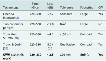
To contextualize the performance of the proposed interconnects within the broader THz integration, Table 2 benchmarks the QWM-slot termination against the most relevant dielectric and metallic interconnection technologies previously reported. In this work, we have proposed and experimentally demonstrated dielectric waveguide terminations for robust interconnection in hybrid-integrated THz systems. In particular, a QWM slot termination enables a compact, contactless interface between substrateless all-silicon dielectric waveguides. Compared to the conventional truncated interconnect [Reference Ichikawa, Gao, Ngo, Ohara, Tanaka, Murakami, Yamada, Yamane, Nishida, Fujita and Nagatsuma28], the QWM-slot termination improves the peak interconnection coupling by approximately  $2.5\,\mathrm{dB}$ across the 220–330 GHz band and maintains a
 $-3\,\mathrm{dB}$ coupling tolerance up to
 $100\,\mu\mathrm{m}$. The three-axis offset characterization further reveals smooth and predictable decoupling over a separation range of approximately
 $1\,\mu\mathrm{m}$. While angular and rotational tolerances remain an important subject for future investigation, the demonstrated three-axis translational robustness already addresses the dominant alignment errors encountered in practical hybrid-integrated sub-THz modules.
Comparison of representative contactless or interface-oriented mm-Waves or THz interconnect approaches

Table 2 Long description
Comparison of five millimeter-wave or terahertz interconnect approaches by operating band, insertion loss, alignment tolerance, physical footprint, and whether they support contactless facilitation across a gap. All entries cover at least 220 to 330 GHz, and one two-conductor port extends to 500 GHz. Lowest reported loss is under 2.0 dB for the two-conductor port, but it is not a gap-based interconnect and is marked as not contactless. Among the contactless options, the fiber to silicon interface reports about 2.2 dB loss but is described as sensitive and has a large footprint. The QWM-slot approach reports about 2.5 dB loss with 100 micrometer tolerance and a sub-wavelength footprint, indicating a compact design with relatively forgiving alignment. Other compact contactless designs show higher loss: truncated silicon dielectric waveguide is about 4.5 dB with under 50 micrometer tolerance, and the truncated plus QWM entry lists two loss values, 5.0 dB and 2.5 dB, with only qualitative tolerance. Tolerance descriptions mix numeric and qualitative terms, so direct ranking of alignment robustness is approximate.
Note:
1 CF: Contactless Facilitation (ability to maintain performance across a physical gap).
2 N/A: Not applicable (metal-assisted port, not a gap-based interconnect).
Beyond the measured performance gains, the QWM slot provides two complementary physical benefits that are central to its robustness. First, it acts as an impedance-matching element, reducing the effective reflection at the interface via a QWM-slot termination [Reference Headland, Kumar, Lees, Withayachumnankul and Carpintero27]. Second, it redistributes the fields into an extended slot aperture, which relaxes the sensitivity to translational offsets and provides leverage in practical packaging and assembly. Together, these effects yield a compact and packaging-tolerant interconnect concept for substrateless silicon dielectric waveguides. A specific application of the proposed QWM-slot interconnect is the contact-free, short-reach routing of sub-THz signals in modular 6G front-ends or multi-chip modules (MCMs). For instance, it can interface a packaged transmitter/receiver IC with a passive all-silicon dielectric-waveguide distribution network feeding a phased-array antenna tile. In such assemblies, thermal expansion, mechanical vibration, and pick-and-place placement errors make sub- $10\,\mu\mathrm{m}$ alignment unrealistic. The measured translational tolerance of up to
 $100\,\mu\mathrm{m}$ at the
 $-3\,\mathrm{dB}$ threshold (Table 1), combined with the compact sub-
 $\lambda$ footprint, enables repeatable module-to-module assembly with relaxed translational alignment requirements. This packaging-oriented approach directly addresses the practical “last-centimeter” interconnect challenges in scalable 6G hardware and high-throughput THz sensing modules.
Acknowledgements
Funding for APC: Universidad Carlos III de Madrid (Agreement CRUE-Madroáo 2026).
Funding statement
This work was supported by the European Union’s Horizon Europe research and innovation program through the Services Joint Undertaking projects SPRINTER (Grant Agreement No. 101070581), TERA6G (Grant Agreement No. 101096949), and POLYNICES (Grant Agreement No. 101070549).
Additional support was provided by the Spanish Ministry of Science and Innovation (MICIU) and the State Research Agency (AEI) through the national grant MiBiLab (ref. PID2023-149035OB-I00), co-funded by ERDF/UE.
Alejandro Lavado Rivera and Daniel Cabo Gallego acknowledge support from the Ayudas para contratos Torres Quevedo program of the Spanish State Research Agency (grant No. PTQ2022-012580 and No. PTQ2022-012583, respectively).
This work also received funding from the Spanish Ministry of Economic Affairs and Digital Transformation and the European Union NextGenerationEU through the project “TERAcom-6G” (ref. TSI-064100-2023-39) within the UNICO I+D 5G-6G 2023 program for research infrastructure and scientific equipment and the EPIC-Pack project (TSI-069100-2023-6).
Competing interests
The authors report no conflict of interest.

Ashish Kumar received his Master’s degree in Optical Engineering from Nanjing University of Science and Technology, China, and his Bachelor’s degree in Electrical and Electronics Engineering from Vel Tech Dr. Rangarajan Dr. Sagunthala R&D Institute of Science and Technology, India. From 2021 to 2024, he was a Marie Skłodowska-Curie Actions Fellow in the TERAOPTICS network, undertaking research secondments at the Center for Physical Sciences and Technology (FTMC), Vilnius, Lithuania. His research interests include terahertz system design, simulation and analysis, dielectric waveguides and waveguide-to-waveguide interconnects.

Muhsin Ali received the B.S. degree in telecommunications engineering from NUCES, Islamabad, Pakistan, in 2011, the M.S. degree in electrical engineering from NUST, Islamabad, in 2013, and the Ph.D. degree in electrical, electronics and automation engineering Universidad Carlos III de Madrid (UC3M), Madrid, Spain, in 2020.
He was a Visiting Researcher with Fraunhofer Heinrich Hertz Institute, Berlin, Germany, in 2019, and the University of Duisburg-Essen, Duisburg, Germany in 2021. He is the co-founder and RF Lead at LeapWave Technologies, a deep-tech company based in Madrid. Currently, he focuses on developing ultra-broadband interconnect technology for instrumentation, sensing and wireless systems markets. His research interests include the design, fabrication and integration aspects of mmWave and THz emitters and detectors for high-speed wireless links with beam-steering capability.

Daniel cabo Gallego received the B.S. degree in physics and the M.S. degree in optoelectronics from the Universidad de Santiago de Compostela, Santiago, Spain, in 2003, and the Ph.D. degree in electronics engineering from Universidad Carlos III de Madrid (UC3M), Madrid, Spain, in 2016.
Since 2022, he is a Co-Founder and led the Photonic Department, LeapWave Technologies, Leganés, Spain. His research interests include terahertz photonics and their applications to sensing and imaging, optoacoustic imaging systems for biomedical applications, high-power short-pulse diode laser instrumentation, optical fiber sensors, and optical detection and generation of high-frequency ultrasounds.

Alejandro Lavado Rivera was born in Madrid, Spain, in October 24, 1984. He received the Engineering degree in telecommunications and the Ph.D. (cum laude) degree in communications from Universidad Carlos III de Madrid (UC3M), Madrid, in 2010 and 2016, respectively. From 2018 to 2022, he was with Yebes Observatory, Dirección General del Instituto Geográfico Nacional, Yebes, Spain. Since 2022, he has been the Chief Technology Officer with LeapWave Technologies, Leganés, Spain. His research interests include dielectric lenses, ultra-broadband terahertz antennas, low-loss terahertz transmission lines, and radio astronomy instrumentation.

Guillermo Carpintero(Senior Member, IEEE) received the Telecommunication Engineering degree from the Universidad Politécnica de Madrid (UPM), Madrid, Spain, 1994, and the Ph.D. degree from the Universidad Carlos III de Madrid (UC3M), Madrid, in 1999. He is currently a Professor with the Electronics Technology Department, UC3M, and the Co-Director of the Optoelectronics and Laser Technology Group (GOTL). He has participated in technical program committees of numerous scientific conferences (ECOC, IRMMW-THz, MWP). His research interests include integrated microwave photonics, hybrid photonic integration, integrated mode-locked lasers, photonic-enabled beam-steered array antennas, integrated Terahertz technology, and high-frequency packaging.
Prof. Carpintero research outcome was recognized with several research awards and distinctions, including the “Doctoral Thesis Extraordinary Award” from UC3M in 2000, “Heather Williamson Young Investigator Award” from International Society for Optics and Photonics in 2000, the UC3M Social Council Excellence Award in 2009, and the 2011 Best European research and Development Project in Cooperation Award from Madri+d Foundation.






 Open access

