





Introduction
The power amplifier (PA) is a key component of the RF transmitter front-end, where high efficiency is critical for effective data transmission. The class-E PA [Reference Sokal and Sokal1] is a widely used switching-mode amplifier, capable in principle of achieving 100% efficiency at maximum saturated output power ( $\mathrm{P_{out}}$), with practical efficiencies of 80% in the sub-6 GHz range at Watt-level power [Reference van der Heijden, Acar and Vromans2, Reference Chen and Peroulis3]. With the advent of 5G and 6G wireless systems, higher data rates and more complex modulation schemes with high peak-to-average power ratios (PAPRs) have emerged. This trend underscores the need for energy-efficient PAs capable of maintaining strong performance over a wide output power back-off (OBO) range of up to 9–12 dB.
Various combinations of class-E PAs have been explored in GaN technologies in the past to achieve high efficiency under back-off conditions. Configurations such as outphasing strategies [Reference Özen, van der Heijden, Acar, Jos and Fager4, Reference Hoffmann, Schellhase, Heinrich and Wentzel5] have exhibited deep OBO up to 10 dB and OBO efficiency in the order of 50%, while Doherty configurations [Reference Lee, Lee and Jeong6–Reference Nghiem and Gajadharsing8] have achieved back-off levels up to 8 dB OBO and OBO efficiency up to 60%. It is therefore of significant interest to continue the research in the field of power-combined class-E PA to achieve even higher efficiency at even higher back-off ranges.
The majority of the solutions reported in the literature employ analog RF signals at the input, while only a limited number utilize a digital input approach [Reference Özen, van der Heijden, Acar, Jos and Fager4, Reference Hoffmann, Schellhase, Heinrich and Wentzel5]. Digital implementations offer greater flexibility and compactness, driving increased interest in fully digital transmitter and PA architectures [Reference Lin, Wu, Chen, Hu, Chen and Zhang9]. The integration of Doherty back-off efficiency enhancement strategy [Reference Doherty10] with the high-efficiency performance of class-E PAs with digital pulse-width-modulated (PWM) input driving remains largely unexplored in the literature. To the authors’ knowledge, the PA presented here is the first example of a GaN-based digital class-E Doherty PA.
Preliminary results of this work were reported at EuMW 2025 and published in the conference proceedings [Reference Bartolotti, Piacibello, Camarchia, Sun, Hoffmann and Wentzel11].
Design process
Two identical digital class-E MMICs (monolithic microwave integrated circuit) [Reference Hoffmann, Schellhase, Heinrich and Wentzel5], fabricated in the Ferdinand-Braun-Institut (FBH) 250 nm GaN-HEMT process, are combined off-chip in a two-way Doherty microstrip combiner to leverage class-E efficiency. A photograph of the fabricated module is shown in Figure 1.
Fabricated digital class-E Doherty module: schematic (left) and photograph (right), showing two GaN PA MMICs and two class-E output networks with the co-designed Doherty combiner. Module size:  $39\times42$ mm2.

Figure 1 Long description
The schematic on the left shows a Class-E Doherty module comprising two GaN PA MMICs, labelled Main MMIC and Aux MMIC, each with a PWM input. Both MMICs integrate on-chip at their output a 0.18 pF shunt capacitor and a 1.25 pF series capacitor. The two paths converge at an off-chip co-designed class-E network and Doherty combiner. Each path includes a 3.3 nH series inductor, a parallel combination of a 39 nH inductor and a 2 pF capacitor, and a 16 nH shunt inductor, followed by the Doherty combiner. The combiner consists of a 40 Ω, 10° line on the Main branch and a 58 Ω, 66° line on the Aux branch, connected to a common node followed by a 36 Ω, 96° line and a 50 Ω, 100° line leading to the RFout port. The photograph on the right shows the fabricated module, with the PWM input, RFout, and co-designed class-E network and combiner labelled. An example bias-line schematic is highlighted, comprising 43 pF, 4.7 µF, and 10 µF capacitors and a 680 nH inductor.
Class-E MMIC
Figure 2 shows the photograph and corresponding schematic of the digital class-E PA chip used in this work, previously presented in [Reference Hoffmann, Schellhase, Heinrich and Wentzel5], with an area of  $1.71\times1.18$ mm2.
Photograph and corresponding schematic of the digital class-E GaN PA MMIC, area  $1.71\times1.18$
 $\mathrm{mm}^2$ [Reference Hoffmann, Schellhase, Heinrich and Wentzel5].

Figure 2 Long description
A digital Class-E GaN PA MMIC comprising three main sections: the first driver stage, voltage-shift stage, and second driver stage, followed by the final stage. The first driver stage includes transistor V01, connected to input IN, resistor R01, and inductor L01. Its active pull-up circuitry comprises transistor V02, capacitor C02 connected to ground, and dumping resistor R02 connected to voltage source Vd1. The voltage-shift stage includes resistor R03 and capacitor C03. The second driver stage includes transistor V03, resistor R05, and inductor L02. Its active pull-up circuitry comprises transistor V04, capacitor C04, and resistor R06 connected to voltage source Vd2. Capacitor C05 and resistor R04 are connected to voltage source −Vs. The final stage includes transistor V1, connected to voltage source VDD, shunt capacitor Cds, and series capacitor C1. The schematic is accompanied by a photograph of the chip layout.
The final stage employs a common-source GaN-HEMT device with dimensions of  $8\times62.5$ µm (V1), preceded by two on-chip driver transistors (V01 and V03 in Figure 2). The drain-source capacitance (
 $\mathrm{C_{ds}}$) of the final device is estimated to be 0.18 pF and provides the required class-E shunt capacitance. At the circuit output, a 1.25 pF series capacitor (C1) is integrated to form part of the class-E output matching network, whose remaining elements are implemented off-chip. The chip operates with three drain supply voltages: a 10 V supply for the final stage (
 $\mathrm{V_{DD}}$) and two 5 V supplies for the driver stages (Vd1 and Vd2). To minimize the number of external supply lines, a voltage-shifting network composed of R03 and C03 is used. C05 provides RF blocking, while R04 damps the resonance formed by C05 and the bias bond wire. Likewise, R02 and R06 damp the resonances associated with C02 and C04 on the drivers’ drain bias lines.
The nominal driving of the digital class-E chip is a PWM signal, which is applied directly to the gate of the first driver transistor (V01). This input controls the switching of V01 and consequently that of the following stages. The chip is switched ON by setting duty cycles different from 0%. In addition, a DC bias voltage of  $-$10 V is applied at the input to set the gate operating point of V01. A shared negative bias (
 $-$Vs), typically set to
 $-$9 V, is applied to the sources of the driver transistors, ensuring that V03 has a sufficiently negative gate resting voltage. This biasing enables large gate swing excursions while maintaining the gate-source voltage (
 $\mathrm{V_{gs}}$) within safe operating limits.
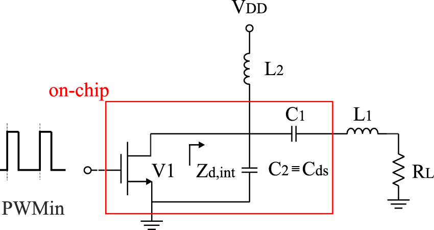
Figure 3 shows the ideal schematic of the class-E output network for the chip’s final-stage transistor (V1 in Figure 1). After the initial component values are derived from Sokal’s design equations [Reference Sokal and Sokal1], the maximum performance of the individual class-E MMIC is evaluated using load-pull simulations in a computer-aided design environment.
Ideal class-E PA with output matching network: MMIC on-chip components are highlighted.

An input PWM excitation with variable duty cycle is used to analyze the optimum loads to be presented at the transistor intrinsic plane (Z $_\mathrm{d,int}$) to achieve the desired power and the highest efficiency at full power and in back-off. In the next section, the selected loads for achieving Doherty load modulation are presented.
The on-chip driver stages (V01 and V03) consume approximately 2 W per chip, significantly affecting the overall efficiency. Since this work aims to demonstrate the effectiveness of the Doherty combining strategy rather than the absolute performance of the standalone digital class-E PA, the reported efficiency values exclude the driver-stage contribution. A chip redesign is underway to address this limitation.
Combiner design strategy
While the switching action of the class-E devices generates multiple harmonics at their drains, in the ideal class-E output network presented in Figure 3, C1 together with part of the inductance L1 forms a resonator tuned to the fundamental frequency [Reference Cripps12], thereby attenuating the harmonics. As a first approximation, only the fundamental frequency reaches the load, thus allowing the application of the Doherty theory developed for linear amplifiers, namely based on the assumption that at the combiner’s plane the current stimulus is sinusoidal and does not contain significant harmonic content [Reference Kim, Kim, Kim and Cha13]. Each PA and the output class-E section formed by (C1–C2, L1–L2) is modeled as an ideal single-frequency current source, and the Doherty theory is applied at the “RL” plane. This section presents the combiner strategy and the selection of the required load impedances, based on ideal single-frequency driving currents (Figure 8(b)). The following section will describe how these driving currents are generated from PWM input signals with varying duty cycles.
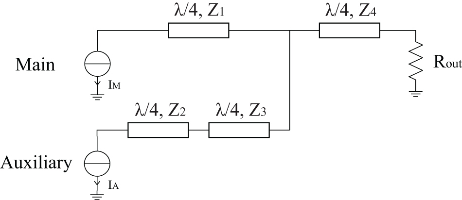
The output combiner strategy from [Reference Xu, Pang, Wang and Zhu14], shown in Figure 4, is adopted. To achieve OBO greater than 6 dB with devices of equal size and identical saturation currents, the generalized Doherty topology incorporates one quarter-wavelength transformer (QWT) in the Main branch, two QWTs with different characteristic impedances on the Auxiliary branch, and one QWT for post-matching. The lines’ characteristic impedances  $\mathrm{Z_1}, \mathrm{Z_2}, \mathrm{Z_3}$, and
 $\mathrm{Z_4}$ constitute the design space. The input variables for the design include the current ratio of the Main amplifier to the Auxiliary amplifier at saturation, defined as
 $\alpha = I_{\text{aux,max}} / I_{\text{main,max}}$, which is set to 1 in this study for equal maximum currents. The OBO level in linear units, denoted as
 $\beta$ and defined in (1), is 0.35 for the 9 dB OBO case.
 \begin{equation}
\beta = 10^{-\mathrm{OBO}/20}
\end{equation}
Generalized Doherty topology from [Reference Xu, Pang, Wang and Zhu14].

The resulting design parameters are expressed in (2) as a function of  $R\mathrm{_{opt}}$, the optimum impedance of the Main amplifier at saturation:
 \begin{equation}
\begin{aligned}
Z_1 &= 1.8\,R_\mathrm{opt}, \quad & Z_2 &= 1.6\,R_\mathrm{opt}, \\
Z_3 &= 1.5\,R_\mathrm{opt}, \quad & Z_4 &= 1.5\,R_\mathrm{opt}.
\end{aligned}
\end{equation}
For the Main amplifier, given the impedance relation at OBO versus saturation (3), the estimation for the output power level at OBO versus saturation (4) can be derived. For the 9 dB OBO target, it results in a reduction of 4.5 dB in power level.
 \begin{equation}
R_\mathrm{opt,OBO} = \frac{1}{\beta}\, R_\mathrm{opt}
\end{equation}
 \begin{equation}
P_\mathrm{out,OBO} = \beta\, P_\mathrm{out,sat}
\end{equation}
Here,  ${R_\mathrm{opt,OBO}}$ is the optimum load impedance of the Main amplifier at OBO, while
 ${P_\mathrm{out,OBO}}$ and
 ${P_\mathrm{out,sat}}$ represent the output power of the Main amplifier at OBO and saturation, respectively.
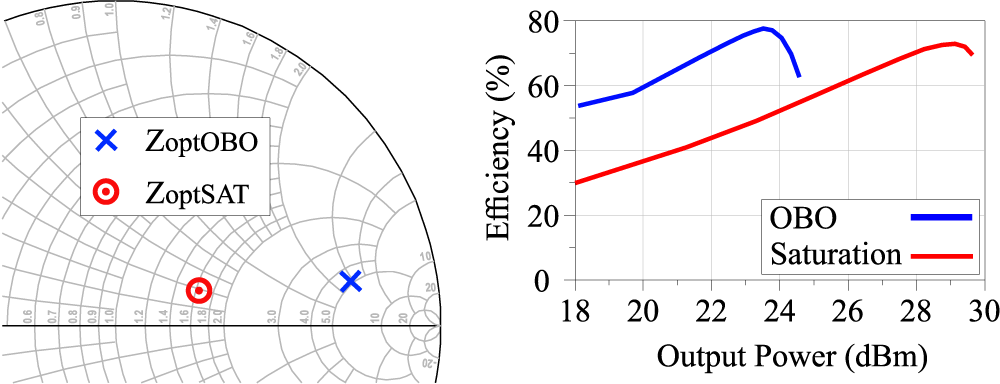
Since the output power of a class-E PA reduces with the duty cycle [Reference Cripps12, Reference Raab15], the reduced output power levels and back-off behavior of the PA are investigated by applying reduced duty cycles at the input. The resulting optimum load at back-off is then verified to satisfy the relationship in (4). At the nominal  $\mathrm{V_{DD}}$ of 10 V, the chip achieves a saturation power of 29 dBm with 70% efficiency on a (77 + j25)
 $\Omega$ load, using a 60% input duty cycle. The optimum load for OBO conditions is evaluated by applying duty cycles below 50%. With a 30% input duty cycle, the load-pull simulations indicate that 75% efficiency can be reached at 24 dBm output power, corresponding to 5 dB back-off, on a (230 + j150)
 $\Omega$ load.
Figure 5 shows the simulated performance of the chip under a swept duty cycle on the optimum loads obtained from load-pull, Z $_\mathrm{opt,SAT}=(77 + j25)\,\Omega$ and Z
 $_\mathrm{opt,OBO}=(230 + j150)\,\Omega$, at saturation and OBO, respectively. The resulting back-off power of 5 dB is sufficiently close to the required 4.5 dB value to satisfy (4).
Chip-level circuit model simulated power-sweep performance at saturation (red) and OBO (blue). Z $_\mathrm{opt,SAT}$ and Z
 $_\mathrm{opt,OBO}$ are highlighted.

Figure 5 shows that a single class-E PA can achieve a certain degree of back-off efficiency enhancement through load modulation. This work aims to demonstrate that a Doherty combination of class-E PAs enables larger back-off levels, on the order of 9 dB, which are more suitable for modern high-PAPR modulation schemes, while also being driven with digital PWM signals.
Figure 1 (left) shows the final implemented combiner together with the class-E output matching networks of each chip. The class-E output network configuration composed by (C1–C2, L1–L2) of Figure 3 is enhanced with the integration on-board of the SMD components (L3, C3) to form a resonator tuned to the second harmonic, in order to reduce the peak voltage across the transistor as demonstrated in [Reference Mediano and Sokal16]. The shunt SMD inductor L4 is introduced to enhance the design space for complex load synthesis.
The combiner strategy presented in [Reference Xu, Pang, Wang and Zhu14] assumes purely real optimum load impedances, whereas the selected optimum loads for class-E operation at saturation and back-off are complex. The combiner lines’ widths and lengths and the values of the off-chip SMD components (C3, L1–L4 in Figure 1) that constitute the class-E output matching networks for each chip have been co-optimized at circuit level. The co-optimization is performed to obtain the optimum loads at the intrinsic drain of the transistors as previously discussed. The final combiner layout deviates from the initial topology shown in Figure 4, with the two transmission lines in the Auxiliary branch merging into a single line and both the Auxiliary and Main branches being implemented with shorter transmission lines. An additional  $50~\Omega$ transmission line is inserted after the combiner solely to enable physical connection to the RF output launcher.
Figure 6 shows the load modulation performance over the (3.2–3.6) GHz bandwidth for the overall simulated module. The target saturation and back-off loads are effectively synthesized. The load modulation trajectories remain well-centered around the target loads across the entire bandwidth.
Load modulation trajectories for the Main (a) and Auxiliary (b) amplifiers over the (3.2–3.6) GHz bandwidth. Simulation of the full digital class-E module.

Figure 6 Long description
The diagram consists of two Smith charts labeled as (a) and (b). In chart (a), the blue trajectory represents the load modulation for the Main amplifier, spanning from 3.2 gigahertz to 3.6 gigahertz. Chart (b) shows the red trajectory for the Auxiliary amplifier, also from 3.2 gigahertz to 3.6 gigahertz. Both charts include markers labeled ZoptBO and ZoptSAT, representing back-off and saturation optimum impedances, respectively. The charts illustrate how the load impedance presented to each amplifier moves with frequency, highlighting differences in trajectory curvature and proximity to the Zopt points.
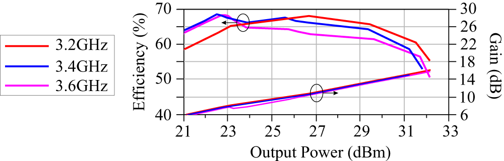
Figure 7 shows the 1-tone simulated output of the full digital class-E module across the (3.2–3.6) GHz bandwidth. The saturated output power ( $\mathrm{P_{sat}}$) exceeds 31.5 dBm with a variation within 0.5 dB.
1-Tone simulated output performance over the (3.2–3.6) GHz bandwidth of the full digital class-E module.

Figure 7 Long description
Legend lists three series: 3.2 gigahertz, 3.4 gigahertz and 3.6 gigahertz. The x-axis is labeled, Output Power (dBm), with tick labels from 21 to 33. The left y-axis is labeled, Efficiency (percent), ranging from 40 to 70 . The right y-axis is labeled, Gain (dB), ranging from 6 to 30. Efficiency curves: At output power 21 dBm, efficiency is about 58 percent for 3.2 gigahertz, about 64 percent for 3.4 gigahertz and about 63 percent for 3.6 gigahertz. Near 23 dBm, all three efficiency curves are near the upper 60s percent, with the 3.4 gigahertz curve highest. From about 23 to 29 dBm, efficiency stays in the mid 60s percent range, with 3.2 gigahertz generally above 3.4 gigahertz and 3.6 gigahertz after about 25 dBm. From about 29 to 32 dBm, all three efficiency curves slope downward, ending near the mid 50s percent range at the highest plotted output power. Gain curves: Gain starts near 6 decibel at 21 dBm for all three frequencies and increases steadily with output power. Around 27 dBm, gain is near 10 decibel. The gain curves end near about 15 to 16 decibel at the highest plotted output power.
The simulated gain exhibits an increasing behavior with output power, consistent with that reported in [Reference Hoffmann, Schellhase, Heinrich and Wentzel5], due to the nearly constant input power of the pulse-driven-wave signal. Efficiency is above 65% at 7.5 dB OBO and above 62% at 9 dB OBO across the bandwidth, peaking at 68% at 9 dB OBO at the center frequency of 3.4 GHz.
Digital driving
In digital class-E amplifiers, varying the input duty cycle allows control of the drain current and output power [Reference Cripps12, Reference Raab15]. In this application, we assume that the fundamental component of the drain current increases linearly with the input duty cycle, analogous to the linear relationship observed in analog-driven PAs between the fundamental drain current and the input drive [Reference Ghione and Pirola17]. Furthermore, we assume that, in the ideal class-E configuration of Figure 3, the fundamental component of the drain current corresponds to the magnitude of the previously assumed single-frequency signal at the load RL, where the Doherty combination theory is applied.
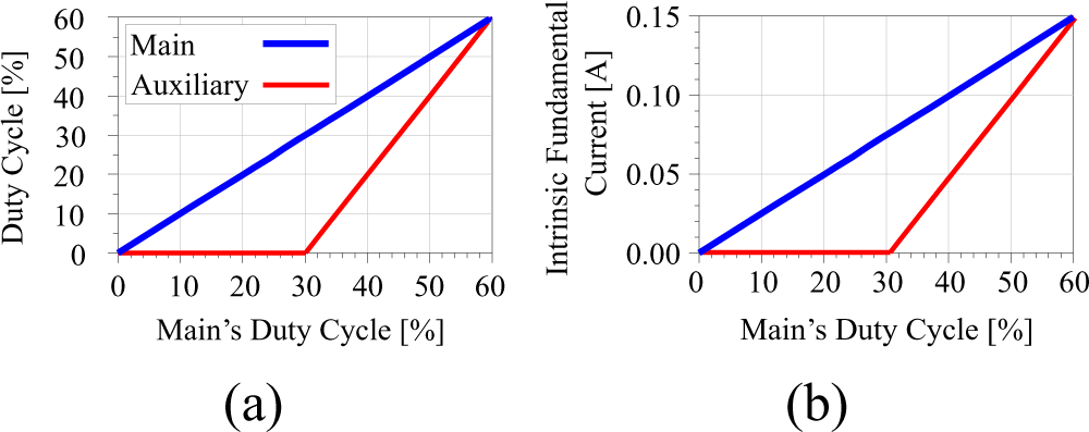
For the implemented digital Doherty, the input duty cycles of the Main and Auxiliary PAs are adjusted to obtain the drain current profiles shown in Figure 8(b). The digital implementation allows precise control of the PA’s turn-on and current ramp by adjusting the input duty cycle. As shown in Figure 8(a), the Main’s duty cycle is set to increase from 0 to 60%. For the Auxiliary device, the duty cycle remains at 0% until the break point, which is located where the duty cycle of the Main reaches 30%, turning the chip on just after this point. It is then increased until the Auxiliary current matches the Main maximum current, as illustrated in Figure 8(b). Digital driving using PWM signals faces inherent limitations, as the minimum achievable duty cycle directly affects the output power dynamic range. Arbitrary waveform generators (AWGs) exhibit a finite time resolution of approximately 10 ps for the M8195A used in this work, limiting the generation of very narrow pulses. This corresponds to a practical duty-cycle resolution of approximately 5% at the design center frequency of 3.4 GHz. Further discussion of these limitations and possible solutions is provided in the following section.
Driving duty cycles (a) and intrinsic fundamental currents (b) ideal target performance for the Main (blue) and Auxiliary (red) PAs.

Figure 8 Long description
Chart (a) shows Main and Auxiliary Duty Cycles values versus Mains Duty Cycle. The horizontal axis label is, Mains Duty Cycle percent, with a range from 0 to 60. The vertical axis label is, Duty Cycle percent, with a range from 0 to 60. Main Duty Cycle coordinate pairs: (0, 0), (60, 60). Auxiliary Duty Cycle coordinate pairs: (0, 0), (30, 0), (60, 60). Chart (b) shows Main and Auxiliary Intrinsic Fundamental Currents values versus Mains Duty Cycle.. The horizontal axis label is, Mains Duty Cycle percent, with a range from 0 to 60. The vertical axis label is, Intrinsic Fundamental Current Ampere, with a range from 0.00 to 0.15. Main coordinate pairs: (0, 0.00), (60, 0.15). Auxiliary coordinate pairs: (0, 0.00), (30, 0.00), (60, 0.15).
Board integration
The module shown in Figure 1 (right) is fabricated on a 0.305 mm Rogers 4003C laminate. The board is mounted on a copper heatsink, and the complete demonstrator measures  $39\times42$ mm2. The two class-E MMICs are mounted in dedicated cutouts on the board, soldered to the copper carrier for common ground and improved heat spreading, and wire-bonded to the DC and RF lines on the PCB. Two RF connectors provide the digital PWM inputs (PWMin), one for the Main chip and one for the Auxiliary chip, each routed to its respective MMIC input via a 50
 $\Omega$ transmission line.
As described in the “Class-E MMIC” section, each MMIC requires four bias lines: three for the drains of the two drivers and final-stage devices, and one for the negative source. The topology of one MMIC bias line is included in Figure 1. It features four decoupling capacitors, ranging from 43 pF to 10 µF, and a feeding inductor. The bias lines are connected to the DC supply via flat-top and pin-header connectors. At the chip outputs, the class-E output network is implemented as described in the “Combiner design strategy” section. The components C1 and C2 are integrated on-chip; L1 and L2 are partially implemented by the gold bond wires necessary to connect the chip to the board; where large values are necessary, high-precision SMD inductors are added on board. Following the class-E networks, the Doherty combiner, realized using microstrip lines, is connected to the RF output (RFout).
Characterization
The measurement setup uses a Keysight M8195A AWG to produce the two digital input signals. Two external broadband preamplifiers generate the minimum peak-to-peak input swing of 6 V required to drive the MMICs’ final-stage transistors. Two bias-Ts are used to supply the gate bias for the first driver transistor, whose gate is directly connected to the PWM input, as shown in Figure 2. At the output, a 20 dB attenuator limits the power delivered to the Tektronix DPO70000SX real-time oscilloscope. All results presented in the following section are derived from the captured real-time waveform data, with power measurements validated using a Keysight UXA spectrum analyzer.
The following biasing conditions are applied: the final-stage device  $\mathrm{V_{DD}}$ is set to 10 V, to match the load-pull simulation performance, while the driver’s drain voltage is set to 5 V. The input gate bias, provided by the bias-Ts, is set to
 $-$10 V to allow large gate swing excursions as described in the “Class-E MMIC” section.
The system was calibrated to equalize the Main and Auxiliary input channels in both amplitude and phase. Nevertheless, a residual phase mismatch may remain at GHz operating frequencies. For this reason, a phase sweep was performed to identify the optimum phase shift between the Main and Auxiliary branches, resulting in an optimal phase difference of 40 $^\circ$ for the co-optimized final circuit shown in Figure 1.
Because the effective gate bias varies with the input duty cycle, the DC level applied through the bias-Ts is dynamically adjusted during single-tone measurements via the remote PC controller to maintain a consistent operating point. This adjustment could not be implemented during modulated signal measurements, since the power supply is controlled via SCPI commands and cannot update the voltage setting on the required time scale. Future work will focus on integrating a GaN-based broadband driver PA with a dynamically adjustable voltage offset like [Reference Hoffmann, Hühn, Shevchenko, Heinrich and Wentzel18] into the digital PA transmitter chain.
The module gain could not be measured due to setup limitations. All reported efficiency values correspond to the drain efficiency of the class-E final-stage transistor only, as the goal of this work is to illustrate the maximum potential of the back-off efficiency enhancement strategy achievable with optimized drivers. The efficiency calculations also exclude the power consumed by the preamplifiers.
1-Tone characterization
The digital Doherty PA has been first evaluated using single-tone PWM input signals to demonstrate the effectiveness of the proposed Doherty combining strategy. The back-off behavior is examined by applying reduced duty-cycle values to the input signals of the Main and Auxiliary chips, following the profiles illustrated in Figure 8.
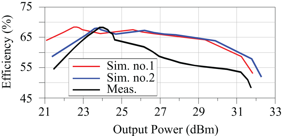
Figure 9 compares the measured and simulated final-stage drain efficiency ( $\eta_\mathrm{drain}$) versus
 $\mathrm{P_{out}}$ at the center frequency of 3.4 GHz. The measured
 $\mathrm{P_{sat}}$ reaches 31.6 dBm, while efficiencies of 68% at 7.5 dB OBO and 61% at 9 dB OBO are achieved.
 $\eta_\mathrm{drain}$ vs. output power performance @
 $f_\mathrm{s}$=3.4 GHz with
 $V_\mathrm{DD}$ = 10 V: 1-tone measured (black) and simulated results with original (red) and improved (blue) MMIC’s output section model.

Comparing the original simulated results (Sim. no. 1) with the measured results (Meas.), a good agreement in the efficiency level is achieved at the back-off peak, while differences appear in the efficiency values throughout the OBO range up to saturation and in the achieved power back-off range. To address this discrepancy, an additional simulation (Sim. no. 2) is performed using a more accurate model of the MMIC output stage, adjusting the simulated values of the output series capacitor C1 and the bond wire connecting it to the board, simulated as L1. In particular, the exact inductance of the bond wires is difficult to determine, introducing some uncertainty in the model; based on measurements, the inductance per unit length is estimated to be approximately 1 nH/mm. The updated simulation provides a better estimate of the OBO efficiency peak, shifting it from 9 to 7.5 dB, while maintaining agreement with the measured OBO efficiency level of 68%.
Despite the improved agreement, a drop in the measured performance is still observed from medium output powers up to saturation. This discrepancy is partly attributed to the simulation approach: the results combine time-domain circuit-level simulations with Doherty combiner losses estimated from electromagnetic simulations. Direct time-domain simulations of the full electromagnetic circuit could be more accurate, but they have shown convergence problems. Furthermore, the board implementation faced grounding issues, which may have affected the measured performance. Overall, the results show that the proposed topology is capable of achieving high efficiency in simulations at 9 dB OBO, as demonstrated by Sim. no. 1 (Figure 9). Updated simulations and measurements confirm the effective achievement of the Doherty efficiency enhancement in back-off, with characterized efficiencies of 68% at 7.5 dB OBO and 61% at 9 dB OBO.
The measured  $\mathrm{P_{sat}}$ has also been characterized for higher
 $\mathrm{V_{DD}}$ values. At a
 $\mathrm{V_{DD}}$ of 12 V, the output power peaks at 32.8 dBm. Nevertheless, according to class-E theory, the maximum voltage swing across the transistor can reach 3.6
 $\times \mathrm{V_{DD}}$ at a 50% duty cycle [Reference Cripps12]. To ensure the robustness of the module during testing, all measurements presented are performed at a
 $\mathrm{V_{DD}}$ of 10 V.
In the measurement setup used, the AWG has a finite time resolution of 16 ps that leads to the minimum duty cycle that was producing output power of about 5%. This corresponded to a characterized minimum output power of 21.5 dBm and 10 dB of output power dynamic range.
One possible approach to overcoming these limitations in digital PWM-driven PAs is currently under investigation and is based on the subharmonic principle [Reference Zhang and Chen19], already used in CMOS-based transmitters. In this approach, at low output power levels, the power devices are switched at a submultiple of the target center frequency, while the desired frequency is generated as a harmonic component of the switching waveform and selected by the filtering behavior of the class-E output network. Since the output is obtained from a higher-order harmonic of the switching signal, lower output power levels can be achieved.
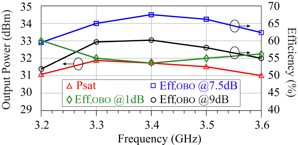
The performance over the (3.2–3.6) GHz frequency range is also investigated using single-tone PWM input signals. Figure 10 shows the maximum output power and peak efficiencies for 1 dB, 7.5 dB and 9 dB OBO levels, across the bandwidth at a  $\mathrm{V_{DD}}$ of 10 V. The saturated output power remains above 31 dBm with less than 1 dB variation over the bandwidth, while the minimum efficiencies achieved at 1, 7.5, and 9 dB OBO, respectively, are 54%, 59% and 52%. Overall, a minimum efficiency of 52% is maintained over the 9 dB OBO range and over a 400 MHz bandwidth, representing a record performance for a digital Doherty amplifier.
1-Tone measured  $\mathrm{P_{sat}}$ and
 $\eta_\mathrm{drain}$ at 1, 7.5, and 9 dB OBO performance with
 $\mathrm{V_{DD}}$=10 V over the (3.2–3.6) GHz band.

Figure 10 Long description
The x-axis is labeled, Frequency (gigahertz), ranging from 3.2 to 3.6 gigahertz. The left y-axis is labeled, Output Power (decibel milliwatt), ranging from 29 to 35 . The right y-axis is labeled, Efficiency (percent), ranging from 40 to 70 . A red triangle series labeled, Psat, is plotted against the left y-axis. The plotted points are at 3.2 equals 31.0, 3.3 equals 31.8, 3.4 equals 31.7, 3.5 equals 31.5 and 3.6 equals 31.0. Three efficiency series are plotted against the right y-axis. A green diamond series labeled, Eff,OBO at 1 decibel, has points at 3.2 equals 60, 3.3 equals 55, 3.4 equals 54, 3.5 equals 55 and 3.6 equals 57. A blue square series labeled, Eff,OBO at 7.5 decibel, has points at 3.2 equals 60, 3.3 equals 65, 3.4 equals 68, 3.5 equals 66 and 3.6 equals 63. A black circle series labeled, Eff,OBO at 9 decibel, has points at 3.2 equals 52, 3.3 equals 60, 3.4 equals 60, 3.5 equals 58 and 3.6 equals 55.
System-level characterization
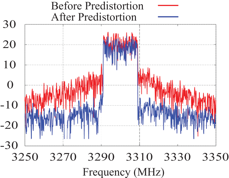
Finally, the PA module is tested across the (3.2–3.6) GHz bandwidth using OFDM input signals with 9 dB PAPR. All input signals are generated using the digital modulator concept presented in [Reference Hühn, Wentzel and Heinrich20], which employs an inline linearization technique that requires no additional power for digital predistortion (DPD). The best results are obtained at 3.3 GHz with a 20 MHz signal bandwidth, achieving 60% average efficiency and 21.6 dBm average power with  $-$20 dBc ACPR. As shown in Figure 11, after linearization, the 20 MHz signal reaches
 $-$31 dBc ACPR and 4.2% EVM, though with reduced efficiency of 47% and output power of 19 dBm. At 3.3 GHz, also the 100 MHz bandwidth has been characterized, achieving 59% average efficiency and 21.4 dBm average power with
 $-$15 dBc ACPR, before DPD.
System-level characterization of 20 MHz, 9 dB PAPR OFDM signal @3.3 GHz before (red) and after (blue) DPD. After DPD,  $-$31 dBc ACPR and 4.2% EVM were achieved, with 47% and 19 dBm average efficiency and average power, respectively.

The linearity performance of  $-$31 dBc achieved by the design remains below the
 $-$45 dBc 5G requirements for the targeted base-station application. In this design, Doherty back-off efficiency enhancement was prioritized over linearity, resulting in low selectivity of the class-E output resonator and degraded linearity. However, literature reports on both analog-driven Doherty [Reference Nghiem and Gajadharsing8] and digitally driven class-E PAs [Reference Özen, Andersson, Eriksson, Acar, Jos and Fager21] demonstrating ACPR values of
 $-$45 dBc or better after linearization. This indicates that the observed linearity limitations stem from the specific implementation and that the presented architecture has potential to fulfill 5G linearity requirements.
From the system-level campaign, a drop in performance of over 10% in average efficiency and 2 dBm in power is apparent. The discrepancy is attributed to the physical limitations of the measurement test bench when used with the nominal digital input drive. Specifically, due to the limited time resolution (16 ps) of the AWG, some short pulses may be lost, and some may be incorrectly generated with reduced amplitude, reducing the total output power and affecting the efficiency. The application of the subharmonic principle [Reference Zhang and Chen19] introduced in the “1-Tone characterization” section, by operating at a lower switching frequency, appears promising for mitigating the loss of short pulses and preventing the performance degradation observed when applying modulated signals. The application of this revised driving approach is planned for future work. Overall, the results nevertheless demonstrate the significant potential of the proposed digital class-E Doherty architecture for future 5G base station applications.
State-of-the-art comparison
The achieved performances are compared to the state-of-the-art of GaN class-E PA in Table 1. Both analog (A) and digital (D) input solutions are considered. Works [Reference Lee, Lee and Jeong6–Reference Nghiem and Gajadharsing8] present Doherty implementations (Impl.) with analog input signals and microstrip combination techniques implemented on-board. Ref. [Reference Ozen, Jos, Andersson, Acar and Fager22] constitutes the only example of a digitally driven class-E PA, where a single class-E MMIC is wire-bonded to an off-chip tunable load matching network implemented with a varactor diode, achieving analogous power levels in the order of 33 dBm.
Comparison with state-of-the-art GaN class-E PAs

Table 1 Long description
Columns list References, Frequency in GHz, Bandwidth (BW) in percent, Saturated power in dBm, Saturated efficiency (eta sat) in percent, OBO efficiency (eta OBO) in percent, OBO in dB, Analog (A) or Digital (D) input, and PA or Doherty PA (DPA) Implementation. Ref. 6 reports 2.14 GHz, negligible bandwidth, Psat 46 dBm, eta sat 75 percent, eta obo 61 percent, OBO 6 dB, A input, Impl. DPA. Ref. 7 reports 2.9 GHz, BW 14 percent, P sat 43 dBm, eta sat 73 percent, eta obo 50 percent, OBO 6 dB, A input, Impl. DPA. Ref. 8 reports 3.6 GHz, BW 11 percent, P sat 48 dBm, eta sat 50 percent, eta obo 54 percent, OBO 7.5 dB, A input, Impl. DPA. Ref. 22 reports 2.0 GHz, BW 10 percent, P sat 33 dBm, eta sat 60 percent, eta obo 40 percent, OBO 6 dB, D input, Impl. PA. This work reports 3.4 GHz, BW 12 percent, P sat 33 dBm, eta sat 48 percent, eta obo 52 percent, OBO 9 dB, D input, Impl. DPA.
This work presents the largest OBO range of 9 dB, with 52% efficiency achieved on a comparable fractional bandwidth in the order of 10%. The comparison shows that the presented implementation is, to the best of our knowledge, the first digitally driven class-E Doherty PA and achieves the highest OBO performance among reported analog- and digital-driven class-E implementations.
Conclusion
This work proposes a GaN-based digital class-E Doherty PA designed for 5G sub-6 GHz applications, achieving peak single-tone performance of 68% drain efficiency at 7.5 dB OBO at 3.4 GHz and maintaining 52% drain efficiency across the (3.2–3.6) GHz band at 9 dB OBO. The compact module demonstrates significant potential for 5G base-station use, delivering efficiencies near 60% when driven with modulated OFDM signals up to 100 MHz bandwidth.
Funding Statement
This work was partly funded by the German BMBF within the “Forschungsfabrik Mikroelektronik Deutschland (FMD)” framework under ref. 16FMD02 as well as within the project “GreenICT@FMD” under ref. 16ME0505. This collaboration was made possible with the support of the European Microwave Association (EuMA) in the context of the 2024 EuMA Internship Award.
Competing interests
The author(s) declare none.

Giulia Bartolotti received her Master’s degree in Electronic Engineering from Politecnico di Torino, Italy, in 2023 with a thesis project on a wideband integrated GaN Doherty power amplifier. She is currently pursuing her PhD at Politecnico di Torino, focusing on designing wideband, multi-stage power amplifiers to enhance efficiency and linearity.

Anna Piacibello received her PhD in Electronic Engineering in 2019 from the Politecnico di Torino, where she is currently an Assistant Professor. She was the recipient of the Young Engineer Prize and of the GaAs Best Student Paper Awards in 2018, and she is a member of the MTT-S TCs 12 (High-Power techniques) and 23 (Wireless communications). Her research interests include the design and characterization of microwave power amplifiers, with a focus on load modulation techniques.

Vittorio Camarchia received the Laurea and Ph.D. degrees in Electronic Engineering from Politecnico di Torino, where he is now an Associate Professor. His research focuses on RF and microwave device modeling, design, and characterization. He has been principal investigator for ESA projects, reviewer for the European Commission, and author of 180 papers, two books, and several book chapters. He chairs the IEEE MTT-S Subcommittee #23 and serves on Subcommittee #12 and the IMS TPRC for power amplifiers. He is an Associate Editor of IEEE MWTL and IEEE Access, and was Guest Editor of the 2020 T-MTT Special Issue on Broadband Millimeter-Wave PAs. He will serve as an IEEE MTT-S Distinguished Microwave Lecturer for 2026–2028. Prof. Camarchia received the 2002 GAAS Young Graduated Research Fellowship.

Deguang Sun(Student Member, IEEE) received the B.Eng. degree in communication engineering from Hainan University, China, in 2020, and the M.Sc. degree in signal processing from Nanyang Technological University, Singapore, in 2022. He is currently a research assistant with the Ferdinand-Braun-Institut (FBH), Germany. His research interests include signal processing for efficient all-digital transmitters and RF modulators.

Thomas Hoffmann received his Diploma from the Technical University of Dresden, Germany. Since 1983, he has worked as a design engineer at the research institute Zentrum für Wissenschaftlichen Gerätebau, in several companies, and as a freelancer. There he developed electronic components and devices for industrial use, particularly switch-mode converters. Since 2008, he has been working for the Ferdinand-Braun-Institut (FBH) in Berlin, Germany, as a research assistant, where he is developing drivers for pulse laser systems and, since 2015, digital power amplifiers.

Andreas Wentzel(M‘16) received the Diploma and the Doctoral degree in electrical engineering from the Technical University of Berlin, Germany, in 2006 and 2011, respectively. Since 2015, he has been the head of the Digital PA Lab in the III-V-Electronics department of the Ferdinand- Braun-Institut in Berlin, Germany. His research activities focus on the design, realization, and measurements of flexible digital TX architectures, including advanced switch-mode power amplifier concepts realized on GaN and InP from GHz to sub-THz, as well as on optimized modulation schemes suitable for these types of PAs. Moreover, his focus is on GaN- and AlN-based highly-efficient VHF power converters up to the GHz range. Dr. Wentzel is a member of IEEE and MTT Society.










 Open access

