
I. INTRODUCTION
The advantage of wide band gap semiconducting materials has been pointed out for high voltage power electronics, where the high electric field strength allows a reduction of the blocking region, to reduce the on-resistance and power losses. Reference Zetterling1,Reference Kimoto and Cooper2 They have also been pointed out as contenders for extreme environment electronics. Reference Cressler and Mantooth3 Because of higher bond strengths much higher radiation doses can be endured. Reference Suvanam, Lanni, Malm, Zetterling and Hallén4
The wide band gap also allows much higher temperature; as it takes more energy before the intrinsic concentration of thermally generated carriers stop the semiconducting operation of diodes and transistors. Reference Zetterling1
At this point in time silicon carbide (SiC) is the most mature wide band gap semiconductor material with commercially available SiC wafers in diameters of 100–200 mm. Reference Kimoto and Cooper2 High voltage capability has been demonstrated with commercial 1.2–1.7 kV devices (diodes and transistors) as well as experimental 10–24 kV devices. Reference Van Brunt, Cheng, O'Loughlin, Richmond, Pala, Palmour, Tipton and Scozzie5 Analog and digital Integrated circuits have been demonstrated experimentally operating at as high temperatures as 400–600 °C Reference Lanni, Malm, Östling and Zetterling6–Reference Ghandi, Chen, Yin, Zhu, Yu, Arthur, Ahmad and Sandvik9 and pressure sensors even up to 800 °C. Reference Okojie, Lukco, Nguyen and Savrun10 This makes application above 300 °C possible, much higher than SOI at 300 °C. Reference Cressler and Mantooth3 In comparison, GaN has mainly shown commercial RF devices and some experimental 4 kV devices. Reference Ohta, Kaneda, Horikiri, Narita, Yoshida, Mishima and Nakamura12 GaN HEMT integrated circuits have been reported to operate up to 500 °C. Reference Gaska, Gaevski, Deng, Jain, Simin and Shur11 Recently integrated circuits have been demonstrated in GaN CMOS technology. Reference Chu, Cao, Chen, Li and Zehnder13
There are many challenges involved when we consider high temperature electronics. Not only do the semiconductors need to be semiconducting at high temperatures, insulators need to be insulating and metals conducting. Chemical reaction should be minimal at these temperatures between SiC and the chosen insulators or metals to assure long-term stability of the materials and reliability of the electronics. As mentioned, SiC is not only semiconducting up to 1000 °C, it is also stable up to 2200 °C. Reference Kimoto and Cooper2 Reactions with oxygen take place at around 1100 °C and SiO2 is stable up to 1400 °C. Reference Kimoto and Cooper2 Insulators are used for interlayer dielectrics, surface passivation and gate oxides; gate oxides are challenging because the applied bias voltage on the thin layers of gate oxides lead to high electric fields. Reference Kimoto and Cooper2
Reactions with metals take place in the temperature range 700 °C and higher. Once formed, most of the metal silicides and metal carbides are stable. Many metals have been tested for ohmic and Schottky contacts, Reference Porter14 but for high temperature operation there are some recent developments using Ni–W. Reference Kragh-Buetow, Okojie, Lukco and Mohney15 For interconnects the reaction with underlying barriers are important to control Reference Lanni, Malm, Zetterling and Östling16 and some systems have been operated for more than 1000 h at 500 °C. Reference Spry, Neudeck, Chen, Lukco, Chang and Beheim7
Once high temperature operation has been achieved, there are requirements for wide temperature range operation, meaning that the electronics can operate from room temperature or lower all the way up to the maximum temperature. Space electronics is one such application, where temperature variations can be from −70 °C in the dark to more than 300 °C in direct sunlight. Reference Cressler and Mantooth3 An additional challenge in terms of reliability can be if the temperature is cycled rapidly, so that the materials undergo many heating and cooling cycles, where differing thermal expansion coefficients can generate mechanical stresses. Packaging is certainly an entirely different challenge, although ceramic packages show some promise. Reference Cressler and Mantooth3
In this paper we will mainly consider the material aspects of designing electronics for a wide temperature range from RT to 500 °C. Digital circuits are easier, since noise margins can usually be increased by increasing the supply voltage. Reference Lanni, Malm, Ostling and Zetterling17 Instead we consider amplifiers, as they are the basic building block for most electronics including power supplies, radio transceivers, instrument amplifiers, and data converters.
The first choice for integrated amplifiers is whether to use (unipolar) field-effect devices or bipolar devices. Both JFET and MOSFET based ICs have been demonstrated at high temperatures. Reference Spry, Neudeck, Chen, Lukco, Chang and Beheim7–Reference Ghandi, Chen, Yin, Zhu, Yu, Arthur, Ahmad and Sandvik9 The main challenge is the threshold voltage variation with temperature that can be in the range of −1 V/100 °C. Reference Kimoto and Cooper2 This therefore requires large threshold and supply voltages at room temperature to maintain normally off operation at 500 °C. One advantage of using bipolar transistors for wide temperature range electronics is that the voltage drift is smaller, in the range −0.2 V/100 °C. Reference Hedayati, Lanni, Rusu and Zetterling18 The built in voltage of the base–emitter junction of 2.5 V requires a large supply voltage, but the relative variation is smaller. The current gain of the bipolar transistor varies with a factor 2–4 in the range 500 °C, but the radiation hardness is better than MOSFETs. Reference Suvanam, Lanni, Malm, Zetterling and Hallén4,Reference Ohshima, Yokoseki, Murata, Matsuda, Mitomo, Abe, Makino, Onoda, Hijikata, Tanaka, Kandori, Okubo and Yoshie19,Reference Nawaz, Zaring, Onoda, Ohshima and Östling20
First we will discuss how basic properties like resistance and transistor gain vary over the temperature range from 27 to 500 °C, based on empirical data rather than theoretical modeling.
Spice models for the different temperatures are demonstrated. Next we will explain negative feedback for the nonelectrical engineer and how it can manage parameter variation of the basic circuit elements (transistors and resistors). The basic tradeoff of gain and bandwidth is explained, and two different circuit designs are presented. In the experimental section we explain the fabrication of the integrated amplifiers in SiC, and how they were measured over the wide temperature range. The measurements are then compared with simulations using the developed models.
II. THEORY
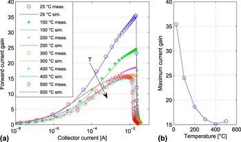
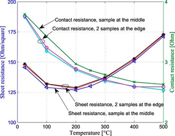
The design of wide temperature range amplifiers can be very challenging. There are many parameters that influence the performance of the amplifier. Doping of the epitaxial layers and their thicknesses vary from batch to batch that result in current gain and sheet resistance variations. In fact, process variation is inevitable and is not a new phenomenon. It was already an issue in vacuum tube electronics and Si transistors. Moreover, the temperature dependence of the device parameters affects the circuit performance at higher temperatures. Current gain of the bipolar transistor is an important parameter of low voltage npn transistors. Based on the experimental data, the current gain of the SiC npn transistor is reduced as the temperature increases from room temperature up to 300 °C, but at higher temperatures, the current gain does not change significantly and it slightly improves up to 500 °C. Similarly, epitaxial integrated resistors in the collector layer vary largely with temperature. The resistance value decreases when the temperature increases from room temperature up to 200 °C, while it increases at higher temperatures. The reasons for these nonmonotonic behaviors are discussed in the Results section.
To achieve an accurate gain amplifier which is independent of process and temperature variations, the amplifiers are used in negative feedback configuration. The amplifier design methodology presented in this paper is based on the negative feedback topology. Negative feedbacks are widely used in amplifier designs because of several remarkable features. First, it produces a stable gain despite temperature changes, process variation, and supply voltage variation. Another advantage is that, the input and output impedances can be tuned for different applications by the proper design of the feedback network. Further, the negative feedback reduces the distortion by comparing a precise attenuated sample of the output signal to the input and suppressing the error. Finally, negative feedback provides higher 3-dB bandwidth.
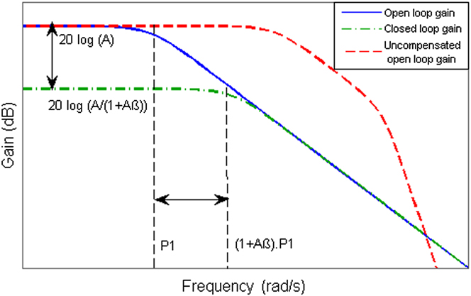
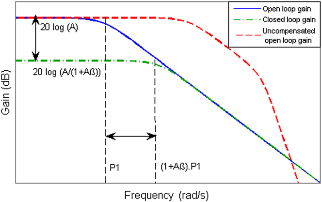
All the mentioned benefits of the negative feedback are achieved at the expense of lower gain and higher risk of oscillation. The stability of the amplifier should be considered in the design phase. The effect of negative feedback on the frequency response and gain of a basic amplifier with a single pole transfer function is illustrated in Fig. 1. When the loop is closed using a feedback network with gain of β, the low frequency gain reduces by a factor of (1 + Aβ) whereas the 3-dB bandwidth increases with the same factor. Therefore, the gain-bandwidth product is always constant. Reference Gray, Hurst, Meyer and Lewis21 The amplifiers such as two-stage amplifiers which are presented in this paper have two or more poles. As mentioned before the negative feedback has a stability issue due to increased bandwidth. One direct method of compensation is to reduce the bandwidth to acquire enough phase-margin at unity gain. In this way, a dominant pole is introduced in the transfer function of the amplifier. For this purpose a capacitor is added to create a dominant pole and limit the bandwidth.
Schematic frequency response of a basic open-loop amplifier and the negative feedback closed-loop amplifier. An uncompensated frequency response is also shown schematically for a multi stage amplifier.
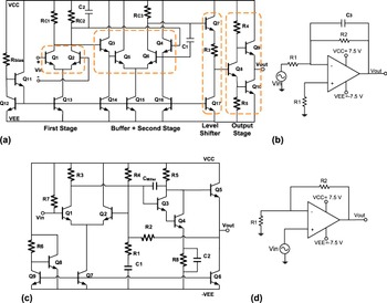
Inverting and noninverting amplifiers are implemented with resistors in the feedback network. This paper compares the simulated and the measured data of two different amplifiers in inverting configuration Reference Hedayati, Lanni, Rodriguez, Malm, Rusu and Zetterling22 and noninverting configuration. Reference Hedayati, Lanni, Rusu and Zetterling23,Reference Hedayati, Lanni, Rusu and Zetterling24 The amplifiers in open-loop and closed-loop configurations are shown in Fig. 2.
SiC operational amplifier in inverting configuration (a) and (b), SiC amplifier in noninverting configuration (c) and (d).

In general, the closed-loop gain of the amplifier is given by
 $${A_{{\rm{CL}}}} = {A \over {1 + A\beta }}\quad ,$$
where A is the open-loop gain of the amplifier and β is the feedback gain. Considering an infinite gain of the amplifier
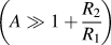 $\left( {A \gg 1 + {{{R_2}} \over {{R_1}}}} \right)$
and zero current to the input of the amplifiers, the ideal closed-loop gain of the amplifiers in inverting and noninverting configurations are defined by the resistors' ratio:
 $${A_{{\rm{CL\_inv}}}} = - {{{R_2}} \over {{R_1}}}\quad ,$$
 $${A_{{\rm{CL\_non - inv}}}} = 1 + {{{R_2}} \over {{R_1}}}\quad .$$
Even if resistor values change with temperature, it is expected that ratio of the resistors made in the same way and located close to each other on chip is constant. The ideal gain is accurate and independent of any kind of temperature changes, open-loop gain variation, or supply voltage variations. However in reality, the open-loop gain is finite and there is always current at the input of the amplifier, the current flows to the base of the input transistors. The amplifiers are composed of two gain stages and an output stage, and Miller capacitances were used to stabilize the amplifiers in feedback. After introducing this compensation capacitor to the circuit, the bandwidth is reduced dramatically. The open-loop gain of the inverting amplifier is given by
 $${A_{{\rm{OL}}}} = {{{I_{{C_1}}}{I_{{C_2}}}{R_{{\rm{eq}}}}\left( {{I_{{C_{5,6}}}}{R_{{C_3}}}} \right)} \over {V_{\rm{T}}^2{I_{{\rm{EE}}}}}}\quad ,$$
where
 $R_{{\rm{eq}}} = R_{C_{1,2} } {\parallel} \left( {r_{\pi _{3,4} } + \beta _{3,4} \left( {r_{\pi _{5,6} } + \beta _{5,6} R_{\rm{E}} } \right)} \right)$
is the effective load and
 ${r_{{\pi _{3,4}}}}$
and
 ${r_{{\pi _{5,6}}}}$
are the input impedances of Q
3,4 and Q
5,6 respectively, and
 ${V_{\rm{T}}} = {{kT} \over q}$
is the thermal voltage.
Likewise, the open-loop gain of the noninverting amplifier is expressed as:
 $${A_{{\rm{OL}}}} = {{{I_{{C_1}}}\left( {{R_2} {\parallel} \left( {{r_{{\pi _3}}} + {\beta _3}{r_{{\pi _4}}}} \right)} \right){I_{{C_4}}}{R_5}} \over {2{V_{\rm{T}}}^2}}\quad .$$
Both expressions show a strong temperature dependence, roughly
 ${1 \over {{T^2}}}$
. Therefore to attain a stable gain, the loop around the amplifier is closed with a feedback network.
III. EXPERIMENTAL
In our in-house SiC bipolar IC process, SPICE Gummel–Poon (SGP) models are developed for the fabricated transistors over the wide temperature range. To mitigate the temperature variation of the components' parameters, amplifier topologies with negative feedback are used. The performance of the designed amplifiers is then verified using the developed SGP models at binned temperature points by simulating the circuits in Cadence software. The new designed circuits are made in 4H-SiC. Then the fabricated circuits are characterized over the wide temperature range and the measured performance is compared to the simulated performance. The methodology is repeated and new improved SGP models are made, and fed back into the new circuit designs.
A set of the SPICE Gummel–Poon (SGP) models for different discrete temperatures have been developed for a SiC npn transistor by using IC-CAP 2014 software. The modeling was performed in two steps. First, the DC parameters and the junction capacitances were extracted from the measured forward and reverse gummel plot and output characteristics of the npn transistor. Second, the extracted parameters were optimized to match the simulated results to the measured data for the binned temperature points: 25, 100, 200, 300, 400, and 500 °C. The models lack ac parameters such as diffusion capacitances. Therefore, the ac performance of the amplifiers is usually overestimated.
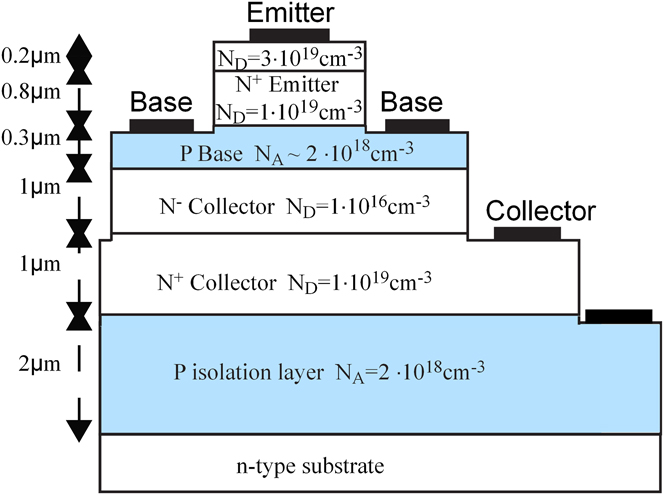
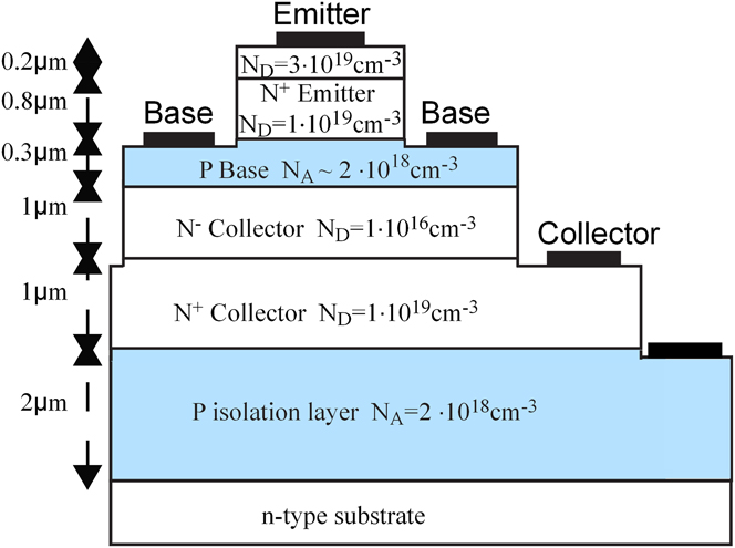
NPN transistors are fabricated on 4-inch wafers with six epitaxial layers. Three mesa etches have been used to form different layers including emitter, base, and collector. The process is ion implantation free to eliminate damage due to ion implantation. The cross-section of a SiC npn transistor with the layers' respective doping concentrations and thicknesses is illustrated in Fig. 3. There are different challenges involved in this IC process such as several etching steps in micrometer range, step coverage for the metallization and reliability of the metallization at 600 °C. Reference Lanni, Malm, Ostling and Zetterling17 Therefore, the performance of bipolar SiC ICs at 600 °C is limited by the metallization, compared to CMOS SiC ICs where the gate oxide reliability is a limiting factor at extreme temperatures. Reference Zetterling1 Higher operating temperature range (up to 1000 °C which is the intrinsic temperature of SiC) can be achieved by improving the metal integrity.
Cross-section of a SiC vertical npn transistor. Reference Lanni, Malm, Ostling and Zetterling17
In our in-house SiC bipolar technology, integrated resistors are implemented in the highly doped collector layer. Transfer length method (TLM) structures with contact size of 100 × 100 μm have been used to extract sheet and contact resistances using four-probe measurements.
The fabricated amplifiers including transistors and resistors, were characterized over the temperature range from 25 °C to 500 °C using on wafer measurements in a high temperature probe station. The microphotograph of the noninverting amplifier and the inverting amplifier are shown in Refs. Reference Hedayati, Lanni, Rodriguez, Malm, Rusu and Zetterling22 and Reference Hedayati, Lanni, Rusu and Zetterling23, respectively. In both circuits, external Miller compensation capacitors were used to stabilize the amplifiers. The stabilization of the inverting amplifier was more challenging due to the higher open-loop gain and also more stages in the amplifier compared to the noninverting amplifier.
In this work the amplifiers are implemented in closed loop configuration with integrated resistors in the feedback network. Therefore, the open-loop gain cannot be measured. However, it can be estimated by measuring the closed loop gain as explained in Ref. Reference Hedayati, Lanni, Rodriguez, Malm, Rusu and Zetterling22.
IV. RESULTS
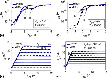
SiC transistors were characterized over the wide temperature range from room temperature to 500 °C. The measured and simulated forward gummel plot and output characteristics of an npn transistor at room temperature and 500 °C are shown in Fig. 4. As illustrated, the simulation results agree with the measurements results which validate the developed SGP models.
Measured and simulated gummel plot of a SiC npn transistor at (a) 25 °C and (b) 500 °C, measurement versus simulation of the output characteristics of a SiC npn transistor at (c) 25 °C and (d) 500 °C.

The measured forward current gain versus collector current that is obtained from the gummel plot is shown in Fig. 5(a). The maximum current gain drops from 35 at room temperature to 15 at 500 °C as shown in Fig. 5(b). Mainly, two effects cause this nonmonotonic temperature variation behavior. The incomplete ionization of the base dopants at room temperature results in current gain reduction up to 300 °C. Whereas above 300 °C, the increased minority carrier lifetime prevents further gain reduction and slightly improves the current gain. Reference Lanni, Malm, Ostling and Zetterling17
(a) Measured current gain of a SiC npn transistor from 25 °C to 500 °C, (b) maximum measured current gain versus temperature.

DC parameters were extracted from forward/reverse gummel plot and output characteristics of the transistor. Table I compares several DC parameters of the developed SGP models at room temperature and 500 °C.
Several Spice model parameters of SiC bipolar transistor.

Figure 6 shows the measured temperature dependence of the sheet resistance and the contact resistance of three TLM samples on two different dies. When the temperature increases up to 200 °C the sheet resistance drops as a result of increased dopant ionization, while at higher temperatures, the resistance value increases due to the decreased mobility. As can be seen in Fig. 6, the temperature variation of the resistors is relatively high (16%) and needs to be considered in the circuit design phase. To alleviate the resistors' variation effect on the gain of the amplifiers and achieving precise and constant gain over the wide temperature range, the amplifiers are used in negative feedback configurations. The closed-loop gain of a negative feedback amplifier relies on the ratio of the feedback resistors rather than the absolute resistor values. Since all the resistors are realized in the collector layer with the same temperature coefficients, the closed-loop gain remains constant over the wide temperature range.
Measured sheet resistance and contact resistance of a TLM structure from 25 °C to 500 °C for three samples.

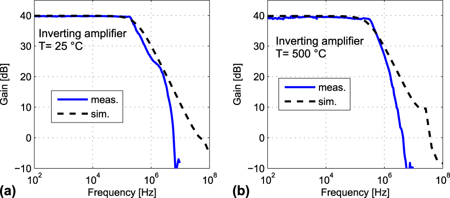
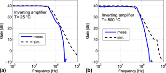
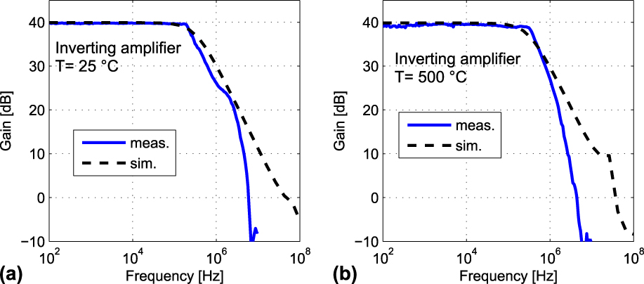
The measured and simulated frequency response of the inverting amplifier at room temperature and 500 °C, are compared in Fig. 7. The simulation results follow the measurement results except for the bandwidth. The simulated 3-dB bandwidth is larger compared to the measured one, due to incomplete AC models and external capacitor of 330 pF in parallel with the integrated 30 pF Miller capacitance. 330 pF can be integrated in new batches therefore the compensation capacitor would be exposed to high temperatures. Increasing the temperature from room temperature up to 500 °C, results in a slight gain reduction. The simulated gain reduces from 39.9 dB to 39.8 dB, while the bandwidth drops from 334 kHz at 25 °C to 315 kHz at 500 °C. The measured gain is reduced slightly from 39.9 dB to 39.5 with increasing temperature from 25 °C to 500 °C.
Measured and simulated frequency response of the inverting amplifier at (a) 25 °C and (b) 500 °C.
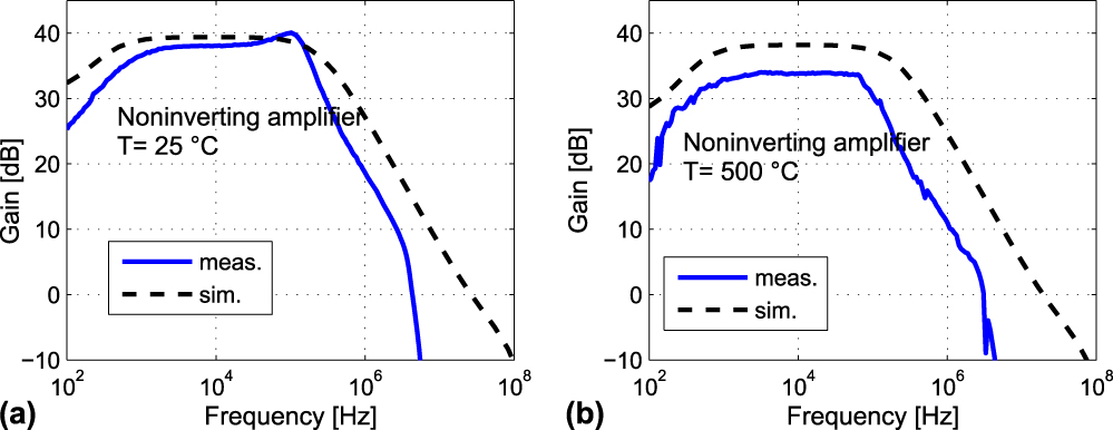
As illustrated in Fig. 8, both simulated gain and 3-dB bandwidth of the noninverting amplifier, reduces from 39 dB to 252 kHz at 25 °C to 38 dB and 210 kHz at 500 °C. Similarly, the measured gain and 3-dB bandwidth of the amplifier decreases from 39 dB to 195 kHz at 25 °C to 34 dB and 100 kHz at 500 °C due to the open-loop gain reduction. As mentioned before, the open-loop gain strongly depends on the operating temperature. The amplifier has relatively low bandwidth which is mainly due to the large Miller compensation capacitor. An external Miller capacitor of 100 pF was required to improve the stability of the amplifier. However as the temperature increases and thus the loop gain decreases, the stability improves. The Miller compensation capacitor of 100 pF can be integrated in SiC while C 1 = C 2 = 1 nF are too large and area consuming and cannot be integrated.
Measured and simulated frequency response of the noninverting amplifier at (a) 25 °C and (b) 500 °C.
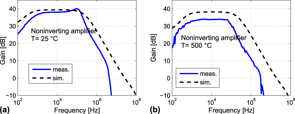
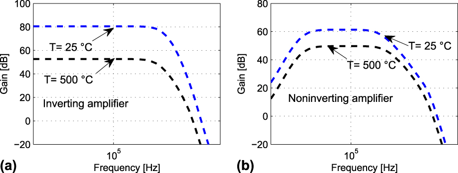
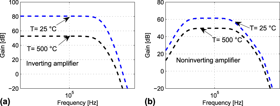
The gain of the noninverting amplifier at 500 °C [Fig. 8(b)] is smaller than the measured gain of the inverting amplifier [Fig. 7(b)] at this temperature, as a result of lower open-loop gain of the noninverting amplifier at 500 °C. The inverting amplifier has more stages and thus as expressed in Eq. (4) has higher open-loop gain compared to the noninverting amplifier. Figure 9 shows the simulated open-loop gain of the inverting and noninverting amplifiers without compensation capacitors. The open-loop gain of the inverting amplifier decreases from 80 dB at room temperature to 52 dB at 500 °C. However, the open-loop gain is high enough to maintain a relatively constant closed-loop gain over the entire temperature range. The simulated open-loop gain of the noninverting amplifier drops from 61 dB to 50 dB when the temperature increases from 25 °C to 500 °C.
Simulated open loop gain of the (a) inverting amplifier and (b) noninverting amplifier.
Two recent works on SiC bipolar amplifier designs are presented in Refs. Reference Kargarrazi, Lanni and Zetterling25 and Reference Tian, Lanni, Rusu and Zetterling26. In Ref. Reference Kargarrazi, Lanni and Zetterling25, a two-stage operational amplifier has been designed using a negative feedback configuration. A low frequency closed-loop gain of about 40 dB has been reported over the wide temperature range from room temperature up to 500 °C. Similarly, in Ref. Reference Tian, Lanni, Rusu and Zetterling26, a fully differential SiC bipolar amplifier in negative feedback configuration with a closed-loop gain of 20 dB has been reported and characterized in the range from 25 °C to 500 °C. These results together with the ones presented in this paper show that the negative feedback is an effective method for wide temperature range amplifiers.
V. CONCLUSIONS
The challenges of the wide temperature amplifier design have been studied. SiC bipolar amplifiers using negative feedback topology have been simulated and characterized from room temperature up to 500 °C. SGP models have been developed at discrete temperature point up to 500 °C. The simulation results based on the developed SGP models have been compared with the measurement results. Despite process variation and wide temperature variation of the transistors and integrated resistors that result in large open loop gain reduction at extreme temperatures, the negative feedback provides a stable gain over the wide temperature range from room temperature to 500 °C. Miller compensation capacitors were required to stabilize the amplifiers at the expense of lower bandwidth. This paper demonstrates that analog circuits can be made in SiC using conventional design techniques.
ACKNOWLEDGMENTS
The Swedish Foundation for Strategic Research (SSF) is acknowledged for funding the HOTSiC project.