Introduction
Quantum phenomena such as superconductivity, charge density waves, skyrmions, magnetic spin ice, and device physics for quantum information science applications are more easily and commonly studied at low temperatures (closer to mK than 77 K).Reference Ball1 In most cases, these phenomena only exist at low temperatures. However, electron microscopes are designed to work optimally at room temperature.
Currently, most ultralow-temperature experimental measurements for quantum materials are performed spectroscopically or with only near-surface imaging. Scanning tunneling microscopy (STM) can provide atomic imaging and electronic structure information with spectroscopic resolution of 11 μeV for exploring quantum phenomena at temperatures down to 10 mK.Reference Assig, Etzkorn, Enders, Stiepany, Ast and Kern2 Scanning tunneling microscopes can provide a wide array of information,Reference Rosenthal, Andrade, Arguello, Fernandes, Xing, Wang, Jin, Millis and Pasupathy3–Reference Pan, O’Neal, Badzey, Chamon, Ding, Engelbrecht, Wang, Eisaki, Uchida, Gupta, Ng, Hudson, Lang and Davis6 providing direct observations of inhomogeneous structures such as charge puddles in graphene at 4.8 KReference Zhang, Brar, Girit, Zettl and Crommie7 and atomic-scale surface features in Weyl semimetals.Reference Zheng, Xu, Bian, Guo, Chang, Sanchez, Belopolski, Lee, Huang, Zhang, Sankar, Alidoust, Chang, Wu, Neupert, Chou, Jeng, Yao, Bansil, Jia, Lin and Hasan8 Beyond the impressive advancements in scanning probe measurement technology of the recent three decades, one of the primary reasons low temperatures provide inherent stability is that as temperatures approach zero K, so do coefficients of thermal expansion. Therefore, even if there is drift and movement, it is small, allowing modern atomic force microscopes and scanning tunneling microscopes to image the same atoms for weeks at a time.Reference Fujita, Schmidt, Kim, Lawler, Hai Lee, Davis, Eisaki and Uchida9 However, scanning probe techniques only provide information from near the sample surface, which by definition cannot provide structural information about internal defects or the three-dimensional microstructure.
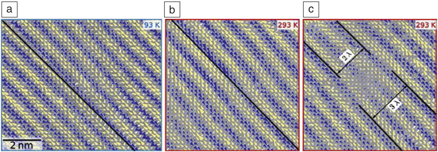
Liquid He-based cryogenic sample stages for electron microscopy have been available since the 1960s.Reference Watanabe and Ishikawa10–Reference Valdrè and Goringe14 While it has been technically possible to cool samples down to as low as 1.5 K in a transmission electron microscope,Reference Fujiyoshi, Mizusaki, Morikawa, Yamagishi, Aoki, Kihara and Harada15 mechanical vibrations and sample drift have limited the resolution, stability, and practical possibilities of ultralow-temperature transmission electron microscopy (TEM). Nonetheless, TEM has been used to image phenomena in quantum materials at more limited resolutions than is available at room temperature. Harada et al. produced the first-ever images of “real-time” observations of vortices in high-Tc superconductors at 9 K.Reference Harada, Matsuda, Bonevich, Igarashi, Kondo, Pozzi, Kawabe and Tonomura16 Mori and colleaguesReference Mori, Chen and Cheong17 used TEM imaging at 95 K to observe patterns of charge localization in the charge-ordered phase of a manganese oxide that displays colossal magnetoresistance. More recently, cryo-transmission electron microscopy (cryo-TEM) with modern electron microscopes has enabled direct imaging of quantum phase transformations in relation to defects and external stimuli. For instance, Carbone and colleagues used Lorentz TEM (a method of phase contrast imaging of magnetic domains) at 7–10 K to observe the formation of skyrmions in Cu2OSeO3 under varying applied electric fields.Reference Rajeswari, Huang, Mancini, Murooka, Latychevskaia, McGrouther, Cantoni, Baldini, White, Magrez, Giamarchi, Rønnow and Carbone18 Zhao and colleaguesReference Zhao, Li, Chang, Jiang, Wu, Liu, Moodera, Zhu and Chan19 recently performed electron energy-loss spectroscopy (EELS) at 10 K using a liquid He stage to understand the role of the substrate on the behavior of the superconductor FeSe. The Kourkoutis group has recently pushed the resolution of cryo-TEM imaging through improvements in image registration to correct for drift Reference Savitzky, El Baggari, Clement, Waite, Goodge, Baek, Sheckelton, Pasco, Nair, Schreiber, Hoffman, Admasu, Kim, Cheong, Bhattacharya, Schlom, McQueen, Hovden and Kourkoutis20 that allowed for not just direct, quantitative imaging of charge order in a manganite, but also observations of their evolutionReference El Baggari, Savitzky, Admasu, Kim, Cheong, Hovden and Kourkoutis21 (see Figure 1).
Atomic resolution mapping charge–lattice coupling in manganite, obtained by cryo-transmission electron microscopy, showing local variations and disorder in an incommensurately ordered charge-stripe phase. (a, b) Picometer-scale shear deformations of striped modulations at (a) 93 K and (b) 293 K. Shear deformation appears as a bending of the wavefronts. The black line traces the direction perpendicular to the modulation wave vector (λ) and helps visualize the deformation of the wavefront. (c) Stripe dislocation at 293 K, in which one wavefront terminates abruptly. The color (i.e., blue, yellow) indicates the direction of modulation, and the size of the arrowheads the magnitude, with the largest distortions, approximately 14 pm.Reference El Baggari, Savitzky, Admasu, Kim, Cheong, Hovden and Kourkoutis21

However, despite these examples of pioneering work on quantum materials, instrument limitations lead to resolution tradeoffs even on the most stable electron microscope platforms. A weakness of modern electron microscopes used in materials science is the side-entry sample-rod design, where the sample is thermally coupled to a cryogenic coolant at the end of the sample rod, leading to short hold times, thermal drift, and coupling to external vibrations. Current high-performance biological cryogenic electron microscopy (cryo-EM) systems have abandoned this design, using a cartridge that is transferred into a cooled stage. These systems used in biology research, unfortunately, lack a five-axis goniometer that is essential for orienting crystalline materials, but they display far superior drift and stability performance. Switching to a mechanically decoupled system will be also be essential for further progress in materials cryo-EM.
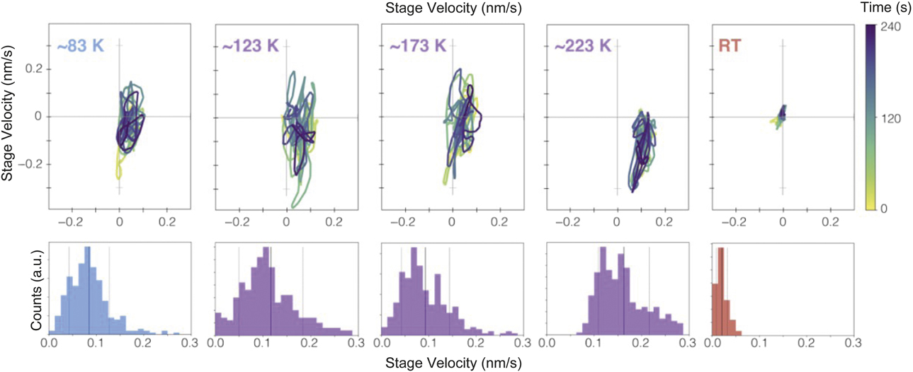
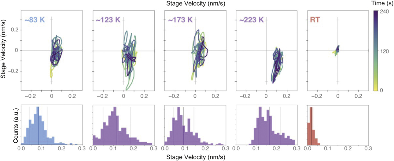
Recent measurements by Goodge et al.Reference Goodge, Bianco, Zandbergen and Kourkoutis22 clearly illustrate that the instantaneous drift velocities for specimen holders cooled below room temperature are substantially worse (Figure 2), as is the settling time to get to the most stable condition at low temperatures. The hold times and vibrations for liquid helium cooling are even worse than for liquid nitrogen. As one of the main strengths of electron microscopy is the ability to measure small (even sub-picometer) lattice distortions in real space, the mechanical instabilities are incredibly limiting.
Stability and drift of a side-entry electron microscopy sample holder when cooled with liquid nitrogen. Relatively stable imaging is achieved across a broad temperature range using a dual-tilt microelectromechanical system (MEMS)-heated variable temperature cryo-holder, although the nitrogen-free room-temperature measurement shows the best performance. (Top row, left to right) Data showing instantaneous stage drift velocities at ∼83 K, 123 K, 173 K, 223 K, and room temperature (RT) tracked over 4 min from registered image stacks. (Bottom row) Corresponding histograms show instantaneous velocity values with the mean (solid line) and standard deviations (dashed line) marked. Holder drift velocities can be somewhat reduced by extending the settling time and by controlling the nitrogen level.Reference Goodge, Bianco, Zandbergen and Kourkoutis22
Given the cost and engineering challenges for designing a stable, low-drift five-axis goniometer, it is worth asking what we could study at ultralow temperatures if we did not have today’s instrumental limitations—especially in temperature regimes rarely explored with high-resolution electron microscopy (i.e., below 77 K) or potentially even in temperature regimes never before explored with electron microscopy (mK).
Electron–lattice coupling
Electron microscopy can unambiguously provide local structural information on the level of individual lattice defects, providing the location of nuclear coordinates to sub-picometer precision, and electronic structure information at the atomic scale, essential for obtaining critical details about electron–lattice couplings. In strongly correlated electronic materials, it has been demonstrated that local complexity can alter critical transitions.Reference Dagotto23 Complexity in this context means microstructure, where features such as local defects, strain fields, and impurities can determine where a transition nucleates and whether it occurs. It has even been suggested that disorder could be considered as an axis for a phase diagram when considering strongly correlated electronic systems such as cuprate- or manganite-based superconductors.Reference Dagotto23 However, in considering the temperature regime of quantum transitions, there is simply much more interest in below liquid nitrogen temperatures (77 K) than above. For example, one of the most widely studied quantum transitions, the critical temperature for superconductivity, is confined to temperatures mostly below 40 K for conventional superconductors (those that can be described by the Bardeen–Cooper–Schrieffer theory24) and below 164 K for unconventional superconductors (such as superconductors based on cuprate and pnictide structures) at atmospheric pressure.Reference Webb, Marsiglio and Hirsch25,Reference Stewart26
Quantum transitions occur through changes in electronic structure. These changes can be imaged using STM techniques, but the correlation with the lattice and electronic structure is not always clear. Electron microscopy should be able to provide more direct structural information across a transition related to quantum criticality, where it is proposed that new phases start as “droplets” of nascent order.Reference Coleman and Schofield27 Structural information with high lattice precision would lead to insights into “remnant behavior” by imaging nucleation events at critical temperatures. For example, it has been recently shown that changes in the T c (critical temperature) of 2H-NbSe2 are affected by strain-induced phase transformations.Reference Wieteska, Foutty, Guguchia, Flicker, Mazel, Fu, Jia, Marianetti, van Wezel and Pasupathy28 TEM could then provide direct observations of the lattice around defects and their associated strain fields at low temperatures, especially with emerging large-field strain mapping techniques such as four-dimensional scanning transmission electron microscopy (4D-STEM).Reference Ozdol, Gammer, Jin, Ercius, Ophus, Ciston and Minor29–Reference Han, Nguyen, Cao, Cueva, Xie, Tate, Purohit, Gruner, Park and Muller31
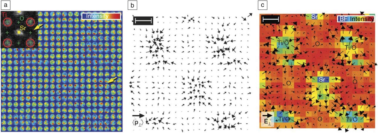
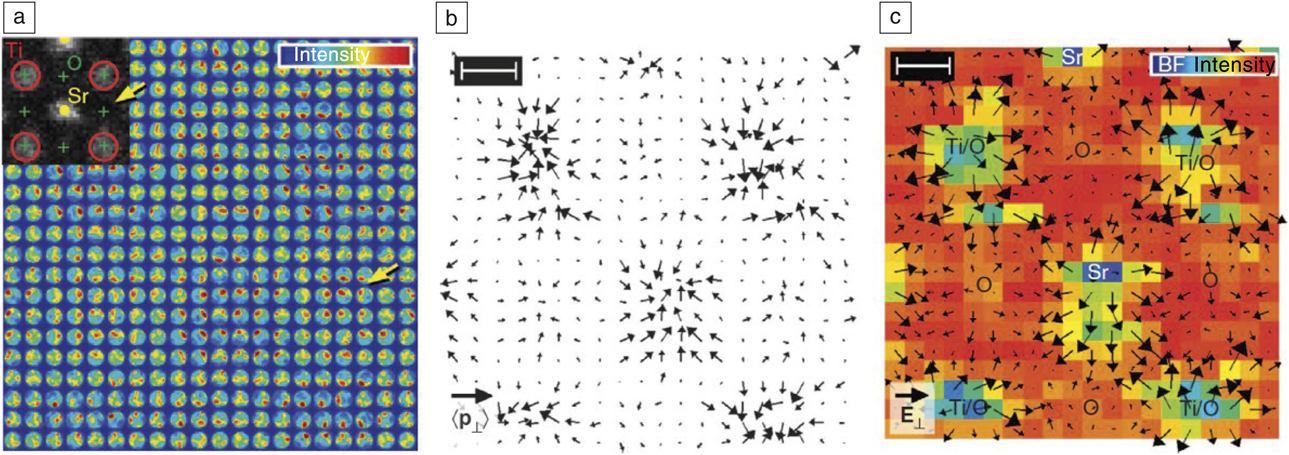
In addition to measuring strain locally with 4D-STEM techniques, it is also possible to measure total charge density and the electric field directly by analyzing momentum transfer to the electron beam in STEM mode (Figure 3).Reference Müller, Krause, Béché, Schowalter, Galioit, Löffler, Verbeeck, Zweck, Schattschneider and Rosenauer32 It is worth considering whether we could spatially resolve the quantum Hall effect by measuring electric fields at atomic resolution or magnetic fields induced by circulating currents at low temperatures.
Imaging of atomic (predominantly the nuclear) electric fields with electron microscopy, demonstrated for SrTiO3. (a) Experimental maps of the central diffraction disks from a probe focused to subatomic dimensions and scanned across a unit cell of SrTiO3 with a 4-min acquisition time. The intensity weighting inside each disk indicates the direction of probability current flow. (Inset) Atomic sites as indexed in the Z-contrast image are recognized in the 20 × 20 array as points of symmetric intensity. An oxygen column is marked by the yellow arrow. (b) Experimental momentum transfer (〈p⊥〉) obtained from (a). Length of the black legend vector is 5 ℏ.nm–1. (c) Electric field, E⊥, derived from the momentum transfer in (b) using the measured specimen thickness of z = 2.5 nm, superimposed on the integrated disk intensity (labeled “BF Intensity” where BF = bright field). Length of the black legend vector is 1 V.pm–1. Scale bars top left in (b, c) = 100 pm and also apply to the image in (a).Reference Müller, Krause, Béché, Schowalter, Galioit, Löffler, Verbeeck, Zweck, Schattschneider and Rosenauer32 Note: ℏ, reduced Planck’s constant.
Magnetic materials
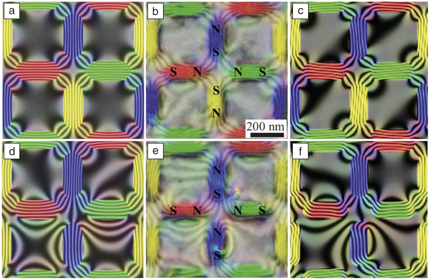
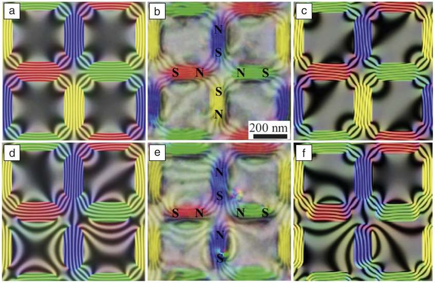
Understanding the low-temperature behavior of magnetic materials can help in the search for new materials operating at technologically relevant temperatures. For example, magnetic-spin ices are a class of materials with interesting and unanswered questions about their structure at very low temperatures. They can have “frustrated” interactions that are not defined by a single minimal energy state. One outstanding question in these materials is whether the spin lattices freeze into a disordered “glassy” state at low temperatures similar to a quantum spin liquid, with a possible connection to high-temperature superconductivity.Reference Ball1,Reference Anderson33 Electron beams undergo phase shifts and deflections when passed through magnetic fields, making them well suited to sensitive, high spatial resolution imaging of magnetic induction fields. Figure 4 shows Lorentz-TEM images from a frustrated two-dimensional square artificial spin-ice lattice at room temperature.Reference Phatak, Petford-Long, Heinonen, Tanase and De Graef34 Understanding the fundamental tetrahedral structure that is thought to lead to magnetic monopoles in real spin-ice crystalsReference Dusad, Kirschner, Hoke, Roberts, Eyal, Flicker, Luke, Blundell and Davis35 would require atomic resolution over a range of temperatures, since the ordering will change as a function of temperature.
The nanoscale magnetic structure of individual magnetic monopoles in an artificially frustrated 2D square spin-ice lattice, obtained using high-resolution aberration-corrected Lorentz transmission electron microscopy at room temperature. The top row shows phase maps with color-coded magnetic induction direction for a neutral node surrounded by four vortices, and the bottom row shows the same for a node with a magnetic monopole defect of positive charge. (a, d) Simulated phase maps using the approximation of uniform magnetization for each element. (b, e) Experimentally obtained high-resolution phase maps. (c, f) Simulated phase maps using micromagnetic simulation data.Reference Phatak, Petford-Long, Heinonen, Tanase and De Graef34 Note: N, North pole; S, South pole of the magnetic dipoles.
Nanophotonics
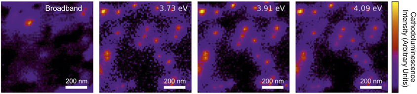
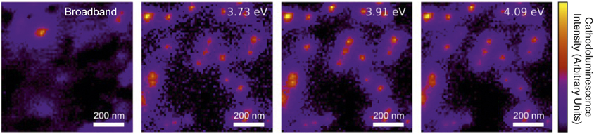
Nanoscale optical measurements take advantage of local confinement and resonance,Reference Baldi, Narayan, Koh and Dionne36 thus electron microscopy is an attractive approach to help identify defects and features of optical signals, especially the simultaneous local characterization of optical response and underlying physical and electronic structure. The lower the temperature for electron-enabled measurements such as cathodoluminescence (electron-beam excited luminescence), the less the contamination, sample damage, nonradiative recombination, and exciton ionization. Bourrellier and colleaguesReference Bourrellier, Meuret, Tararan, Stéphan, Kociak, Tizei and Zobelli37 used low-temperature (150 K) cathodoluminescence measurements in a scanning transmission electron microscope to identify a new extremely bright UV single-photon emitter (4.1 eV) in hexagonal boron nitride. Figure 5 shows hyperspectral cathodoluminescence maps from this work confirming high spatial localization of the emission indicating a point defect origin.Reference Bourrellier, Meuret, Tararan, Stéphan, Kociak, Tizei and Zobelli37 Electron microscopy has already demonstrated the ability to manipulate single dopant atomsReference Hudak, Song, Sims, Troparevsky, Humble, Pantelides, Snijders and Lupini38 and fabricate structures at the atomic level.Reference Hudak, Song, Sims, Troparevsky, Humble, Pantelides, Snijders and Lupini38,Reference Kalinin and Pennycook39 Ultralow-temperature electron microscopy has the potential to place defects where we want them, know what they are, and measure their optoelectronic effects in situ.
Spatially resolved cathodoluminescence intensity maps of bright, ultraviolet single-photon emitters in hexagonal boron nitride measured in a scanning transmission electron microscope at 150 K. The perfect spatial correlation of the emission peaks at 3.73, 3.91, and 4.09 eV suggests the same underlying physical origin, in this case a phonon replica of the 4.09 eV peak. The color bar represents cathodoluminescence intensity (arbitrary units).Reference Bourrellier, Meuret, Tararan, Stéphan, Kociak, Tizei and Zobelli37
Quantum information science
Electron microscopy has had an enormous impact on device characterization and failure analysis for integrated circuits. Primarily, this has come from room-temperature microscopy, which is close to the operating temperatures of most electronic devices. However, to have the same impact on low-temperature device physics, such as is relevant to the emerging field of quantum information science, it is imperative to analyze materials at their actual operating temperature. At extremely low temperatures where qubits (quantum bits) operate, it is unknown precisely how adsorbates, strain, and interfacial materials characteristics affect materials properties, and thereby device characteristics.Reference Ani Nersisyan, Alidoust, Manenti, Renzas, Bui, Vu, Whyland, Mohan, Sete, Stanwyck, Bestwick and Reagor40 Barkov et al.Reference Barkov, Romanenko, Trenikhina and Grassellino41 showed how large island-shaped hydrides that appeared at low temperatures in Nb superconducting cavities led to the emergence of “Q disease,” the deterioration of the quality factor. Cryo-electron microscopy can provide not only structural and electronic properties for such defects, but also imaging of vortices and flux pinning at defects, grain boundaries, and interfaces.Reference Harada, Matsuda, Bonevich, Igarashi, Kondo, Pozzi, Kawabe and Tonomura16
Opportunities for correlative microscopies
Understanding the structure and chemistry of materials requires both high spatial resolution and high-energy resolution of the outgoing scattered probe particle. Electron optics makes atomic imaging possible, with energy resolution below 10 meV,Reference Lagos and Batson42 whereas x-ray optics offer easier ensemble measurements of large fields of view for more representative statistics. Correlative microscopy at low temperatures can thus bridge length scales and provide complementary information. Electron and x-ray techniques generally have analogs—such as STEM/scanning transmission x-ray microscopy. For chemical analysis, EELS and x-ray absorption spectroscopy both provide useful core loss information.Reference Goode, Porter, Ryan and McComb43 Soft x-ray resonant inelastic x-ray scattering is approaching 10 meV resolution at 1 keVReference Jarrige, Bisogni, Zhu, Leonhardt and Dvorak44 at modern, diffraction-limited storage ring x-ray sources. New, high repetition rate x-ray free-electron lasers have the potential,Reference Bostedt, Bozek, Bucksbaum, Coffee, Hastings, Huang, Lee, Schorb, Corlett, Denes, Emma, Falcone, Schoenlein, Doumy, Kanter, Kraessig, Southworth, Young, Fang, Hoener, Berrah, Roedig and DiMauro45 with suitable temporal coherence, to further extend energy and temporal resolution. Correlative microscopy offers paths to ultimate spatial and energy resolution. At very low temperatures, both spatial and spectroscopic resolution are exciting new frontiers. The combination of electron and x-ray microscopies can reach these limits. If very low temperature electron sources are capable of low intrinsic energy spread or high coherence, then it is possible that atomic resolution imaging with exquisite energy resolution and coherence can be achieved in an electron microscope.
Summary
Atomic resolution electron microscopy at cryogenic temperatures without the current design limitations in spatial or spectral resolution would enable dramatic advances in understanding structure–property relationships in quantum science. Resolution is critical for direct observations of quantum phenomena, since lattice distortions on the level of picometers can characterize an electronic phase transformation. Reaching this goal is not limited by fundamental physics, but rather by engineering and instrumentation challenges, which will require new investments in cryogenic electron microscope designs optimized for low-temperature materials science.
Acknowledgments
The content of this article is based on a workshop held in Berkeley, Calif., in January 2019. We would like to thank all of the workshop participants for contributing to the discussions that led to this article, especially the invited speakers: L. Kourkourtis, A. Pasupathy, K. Müller-Caspary, A. Petford-Long, J. Cha, J. Analytis, R. Ramesh, P. Crozier, C. Regan, A. Salleo, Y. Zhu, J. Idrobo, M. Kociak, and J. Dionne. A.M. and the workshop were supported by the Molecular Foundry, which is supported by the Office of Science, Office of Basic Energy Sciences, of the US Department of Energy (DOE) under Contract No. DE-AC02–05CH11231. A.M. was also supported by the DOE, Office of Science, Basic Energy Sciences, Materials Sciences and Engineering Division under Contract No. DE-AC02–05-CH11231 within the High-Coherence Multilayer Superconducting Structures for Large Scale Qubit Integration and Photonic Transduction Program. P.D. acknowledges support by the DOE, Office of Science, Basic Energy Sciences, Scientific User Facilities Division under Contract No. DE-AC02–05-CH11231. D.M. also acknowledges support from the US National Science Foundation (NSF) through the PARADIM materials innovation platform under Cooperative Agreement No. DMR-1539918, and the Cornell Center for Materials Research, an NSF materials research science and engineering center (Grant No. DMR-1719875).

Andrew Minor is a professor of materials science and engineering at the University of California, Berkeley, and is also the facility director of the National Center for Electron Microscopy in the Molecular Foundry at Lawrence Berkeley National Laboratory. He received his BA degree from Yale University in economics and mechanical engineering in 1997, and his MS and PhD degrees in materials science and engineering from the University of California, Berkeley, in 2000 and 2002, respectively. Minor has co-authored more than 190 publications and presented more than 130 invited talks on topics such as nanomechanics, lightweight alloy development, characterization of soft materials, and in situ transmission electron microscopy technique development. His awards include the Lawrence Berkeley National Laboratory Materials Science Division Outstanding Performance Award (2006 and 2010), the AIME Robert Lansing Hardy Award from The Minerals, Metals & Materials Society (2012), and the Burton Medal from the Microscopy Society of America (2015). Minor can be reached by email at aminor@berkeley.edu.

Peter Denes has been a senior scientist at Lawrence Berkeley National Laboratory since 2000. He received his PhD degree in physics in 1984 from The University of New Mexico. He was a senior research scholar at Princeton University in the Department of Physics. His research interests include instrumentation to improve microscopies, such as the development of complementary metal oxide semiconductor direct electron detectors. He has published more than 500 papers, and his awards include the 2017 Joseph F. Keithley Award for Advances in Measurement Science from the American Physical Society and the 2015 Berkeley Lab Lifetime Achievement Award. Denes can be reached by email at pdenes@lbl.gov.

David Muller is the Samuel B. Eckert Professor of Engineering in the School of Applied and Engineering Physics at Cornell University, and co-director of the Kavli Institute for Nanoscale Science at Cornell University. He received his BSc degree from The University of Sydney, Australia, in 1991, and his PhD degree from Cornell University in 1996. He was previously a member of the technical staff at Bell Labs. His current research interests include hardware and algorithms for high-speed pixelated detectors for imaging beyond the diffraction limit, and the atomic-scale control and characterization of matter for applications in energy storage and conversion. He is a Fellow of both the American Physical Society and the Microscopy Society of America, and recipient of the Microscopy Society of America Burton Medal and Microanalysis Society Peter Duncumb Award for Excellence in Microanalysis. Muller can be reached by email at dm24@cornell.edu.