Introduction
Inspired by the potential to solve problems that cannot be efficiently solved by any classical computer, researchers have exerted enormous effort in the last two decades to develop a quantum computer.Reference Nielsen and Chuang1 Data processing in a quantum computer is performed through the manipulation of quantum information, the fundamental unit of which is called (by analogy with classical computation) a qubit. Conceptually, a qubit is a quantum mechanical system that can be in any linear combination α|0> + β|1> (where α and β are complex numbers representing probability amplitudes) of two fundamental basis states, denoted as |0> and |1>. Given the restriction that |α|2 + |β|2 = 1, the state of the qubit is often represented schematically by a point on a unit sphere (the “Bloch sphere”). The state of the qubit (i.e., its position on the Bloch sphere) can be manipulated through appropriate physical operations, and by allowing qubits to interact with one another, the states of multiple qubits can become entangled.
A detailed discussion of these manipulations and interactions is beyond the scope of the present article, but two points warrant emphasis: In order for the qubit to function well, the basis states should be unique and energetically distinct from other states accessible to the system, and unintentional perturbations of the system by its environment should be minimized. Physical embodiments of qubits have included the polarization states of photons; the energy levels of trapped ions; the nuclear spins in molecules; the spin states of confined electrons in solids; and the charge, flux, or phase of pairs of electrons bound together at low temperature (Cooper pairs) in superconducting materials.Reference Ladd, Jelezko, Laflamme, Nakamura, Monroe and O’Brien2
In semiconductors, qubits have been realized by electrons confined to point defects, such as nitrogen-vacancy centers in diamond and phosphorus donors in silicon, and to self-assembled nanostructures.Reference Morello, Pla, Zwanenburg, Chan, Tan, Huebl, Möttönen, Nugroho, Yang, van Donkelaar, Alves, Jamieson, Escott, Hollenberg, Clark and Dzurak3 An alternative approach is to first confine electrons within a two-dimensional (2D) quantum well, and then to apply biases to gates above the well to enclose the electrons within an electrostatically defined quantum dot. In this approach, quantum information can be encoded in the spin state of one or more electrons confined to the quantum dot. This approach has been implemented in very high-quality GaAs/AlGaAs heterostructures,Reference Petta, Johnson, Taylor, Laird, Yacoby, Lukin, Marcus, Hanson and Gossard4 GaInAs quantum wells,Reference Croke, Borselli, Gyure, Bui, Milosavljevic, Ross, Schmitz and Hunter5 silicon metal oxide semiconductor nanostructures,Reference Nordberg, Ten Eyck, Stalford, Muller, Young, Eng, Tracy, Childs, Wendt, Grubbs, Stevens, Lilly, Eriksson and Carroll6 and Si/SiGe heterostructures.Reference Maune, Borselli, Huang, Ladd, Deelman, Holabird, Kiselev, Alvarado-Rodriguez, Ross, Schmitz, Sokolich, Watson, Gyure and Hunter7 All but the last of these implementations are able to make use of high-quality, single-crystal substrates on which the active device layers can be grown coherently and pseudomorphically, without the complication of plastic deformation. That is not the case with the Si/SiGe system, although it has seen remarkable progress in recent years.Reference Zwanenburg, Dzurak, Morello, Simmons, Hollenberg, Klimeck, Rogge, Coppersmith and Eriksson8
Quantum devices implemented in the Si/SiGe system rely on metamorphic substrates—strain-relaxed, compositionally graded films of SiGe on which the active device layers are deposited. The discussion that follows focuses on this system and on the possible limitations imposed on device performance as a result of the metamorphic substrate. We note, however, that other embodiments of qubits also employ metamorphic films. In particular, microwave resonators and Josephson junctions that are critical elements in superconducting quantum architectures contain several metal–dielectric interfaces, and good device performance relies on the optimization of metamorphic metal films grown on a dielectric.Reference Megrant, Neill, Barends, Chiaro, Chen, Feigl, Kelly, Lucero, Mariantoni, O’Malley, Sank, Vainsencher, Wenner, White, Yin, Zhao, Palmstrøm, Martinis and Cleland9 The section on metamorphic materials for superconducting qubits discusses some of the approaches used in these applications.
Approaches based on Si/SiGe heterostructures
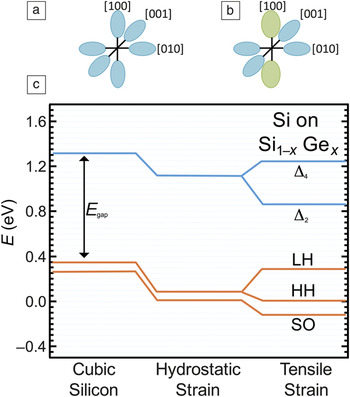
The bandgap of bulk Si is larger than that of SiGe, and one would expect that as these materials are brought into contact with each other, the conduction-band edge of Si would lie above that of SiGe, and the valence-band edge would lie below that of SiGe. This type of band alignment is termed Type I. However, the band edges for Si films embedded in (100)-oriented, unstrained Si1–xGex exhibit a Type-II band alignment.Reference Abstreiter, Brugger, Wolf, Jorke and Herzog10 That is, while the bandgap of silicon remains larger than that of the surrounding Si1–xGex, the biaxial, tensile strain imposed on the Si film decreases the energy of its conduction-band edge relative to that of the unstrained Si1–xGex.Reference Abstreiter, Brugger, Wolf, Jorke and Herzog10 It is this band alignment that enables quantum confinement in Si/SiGe buried-channel structures. As the Ge mole fraction increases from 0 to some value x, the inherent, sixfold conduction-band degeneracy of bulk, unstrained Si is lifted, with four equivalent in-plane valleys, Δ4, rising in energy, and two equivalent out-of-plane valleys, Δ2, lowering in energy at twice the rate of the Δ4 valleys.Reference Schäffler11 This process is illustrated schematically in Figure 1. The Si layer acts as a quantum well, and electrons, supplied either through applied voltages or by layers in the Si1–xGex that are doped n-type, are confined to 2D electron gases at the Si/SiGe interfaces.
Fermi surfaces for (a) cubic silicon and (b) silicon grown on SiGe[100] and under biaxial tensile strain. The ellipsoids represent areas of constant energy—the lifting of the sixfold degeneracy with strain is illustrated by the change in color and shape of the [100]-oriented ellipsoids in (b). (c) The respective effects of hydrostatic and biaxial tensile strain on the valence and conduction bands of silicon, illustrating the use of strain to eliminate degenerate states. Adapted with permission from Reference Reference Schäffler11. © 1997 Institute of Physics. Note: E gap, bandgap energy; E, energy; Δ4, fourfold degenerate in-plane conduction band; Δ2, twofold degenerate out-of-plane conduction band; LH, light hole valence band; HH, heavy hole valence band; SO, spin–orbit split band.

Strained silicon n-metal oxide semiconductor field-effect transistor devices have achieved enhanced mobility by exploiting the fact that the in-plane, effective mass of the electrons in the Δ2 valleys is reduced relative to their bulk value, as is the intervalley phonon scattering.Reference Schäffler11–Reference Paul13 In the context of electrostatically defined quantum dots for computing applications, the formation of the Si well provides confinement in one dimension, and the splitting of the sixfold degenerate valleys is an important step towards the definition of a nondegenerate ground state. Splitting of the remaining twofold degeneracy in the Δ2 valleys is critical to the definition of a nondegenerate ground state, and is discussed later in this article.
We must first note that the composition range typically used in these structures has Ge mole fractions x on the order of 0.20–0.35. This range provides conduction-band offsets between the Si well and the SixGe1–x cladding of roughly 100–200 meV. Larger values of x could be used, but doing so would impose severe constraints on the thickness of the Si well due to strain considerations.
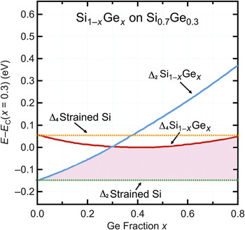
Figure 2 illustrates the Δ2 and Δ4 conduction-band offsets for silicon grown on top of a Si0.7Ge0.3 buffer; also displayed are the offsets for a SixGe1–x-cap layer subsequently grown on top of the silicon. The composition of the cap is normally chosen to be identical to that of the buffer. In any event, no bulk SiGe crystals of high quality and with reasonable size exist in this composition range. Several groups have attempted to grow single crystals of SixGe1–x, but typically only in the composition ranges 0 < x < 0.15 and 0.85 < x < 1.Reference Usami, Shiraki and Usami14–Reference Dold, Barz, Recha, Pressel, Franz and Benz18 Researchers suspect that, outside of these composition ranges and despite the fact that Si and Ge are miscible for all x, the large difference in physical properties between Si and Ge atoms makes it difficult to grow large, defect-free single crystals.Reference Yildiz, Dost and Lent15 Segregation during growth and distinctly different Si–Si, Si–Ge, and Ge–Ge bond lengths result in built-in strain that causes the crystals to be polycrystalline rather than a single crystal.Reference Usami, Shiraki and Usami14,Reference Yonenaga19,Reference Yonenaga, Sakurai, Sluiter, Kawazoe and Muto20 Although high-quality Si0.5Ge0.5 single crystals two inches in diameter were recently prepared using the traveling liquidus-zone method, it is unclear if this method would work to achieve the Ge compositions needed for quantum-computing applications.Reference Kinoshita, Arai, Nakatsuka, Taguchi, Tomioka, Tanaka and Yoda21
Conduction-band offsets, relative to the substrate, for Si and Si1–xGex films grown pseudomorphically on a Si0.7Ge0.3 strain-relaxed buffer. For the Si film, the Δ2 twofold degenerate conduction-band valley minima (green dotted line) and the Δ4 fourfold degenerate conduction-band valley minima (orange dotted line) are constants; for the Si1–xGex film, they vary with x. The shaded region denotes the offset between the Si and Si1–xGex films. Thus, controlling the relative composition between a metamorphic substrate and epitaxial layers facilitates precise bandgap engineering. Adapted with permission from Reference Reference Schäffler11. © 1997 Institute of Physics.

Not having SixGe1–x wafers with the desired alloy composition necessitates the use of metamorphic, strain-relaxed buffers as substrates for the growth of device layers. This growth is generally performed by chemical vapor deposition (CVD) or molecular beam epitaxy (MBE) on Si substrates, and considerable effort has gone toward optimizing the growth process.Reference Lee, Fitzgerald, Bulsara, Currie and Lochtefeld22 If the target composition of Si1–xGex were directly deposited onto the Si substrate, a dense network of dislocations would form once the film thickness exceeded the critical thickness for their formation.Reference Matthews and Blakeslee23 Each dislocation would consist of a strain-relieving misfit segment parallel to the growth plane and two threading segments running up to the surface of the film (unless one or both ends managed to run to the edge of the wafer first). Each dislocation would attempt to maximize the length of its strain-relieving misfit segment parallel to the growth plane in order to maximize relaxation, but it would be prevented in doing so by interactions with neighboring dislocations. The result would be a dense network of short misfit dislocations near the interface with the Si substrate and a high density of threading dislocation segments running up through the buffer and the device layers, potentially acting as mobility-limiting scattering centers in the Si well.Reference Monroe, Xie, Fitzgerald, Silverman and Watson24 For the Ge mole fractions of interest, threading dislocation densities on the order of 109–1011 cm–2 have been observed.Reference Schäffler11
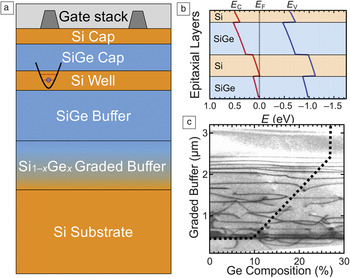
To prevent strain-relieving dislocations from forming all at once, Si1–xGex films are compositionally graded from x ≈ 0 at the Si substrate to x = x f at the top of the buffer, as illustrated in Figure 3. This grade is typically achieved through a monotonic increase in the concentration at a rate of approximately 10% Ge per micrometer, but may be performed in steps and may involve more complicated concentration profiles. To maximize dislocation glide velocity, the growth temperature is also chosen to be as high as possible. Threading dislocation densities on the order of 106 cm–2 have been achieved through these approaches.Reference Lee, Fitzgerald, Bulsara, Currie and Lochtefeld22
Schematic cross section of an epitaxial layer stack. (a) Gate electrodes on the semiconductor surface are employed to accumulate and manipulate electrons in the silicon well. (b) The conduction- (red) and valence- (blue) band edges and Fermi level (black dashed line) of the epistructure are displayed as a function of depth. The epilayers are color matched with the corresponding layer featured in (a). (c) Cross-sectional transmission electron microscope image showing a network of strain-relieving dislocations throughout the graded buffer and their absence in the constant-composition region at the top of the buffer. The dotted line indicates the Ge mole fraction as a function of depth. Reprinted with permission from Reference Reference Schäffler11. © 1997 Institute of Physics. Note: E C, conduction-band energy; E F, Fermi energy level; E V, valence-band energy; E, energy.

The nucleation of new dislocations and the interaction of propagating dislocation segments interact in a complicated way with the evolving growth surface, thus resulting in a rough final surface morphology that exhibits a characteristic crosshatch morphology.Reference Currie, Samavedam, Langdo, Leitz and Fitzgerald25 This roughness presents not only a practical challenge to the subsequent lithographic definition of electrostatic gates on the final device layers, but also a fundamental obstacle to the operation of quantum dot devices. The high areal density of atomic steps comprising the crosshatched surface will propagate up to the Si channel layer and impede the splitting of the Δ2 valley degeneracy. While very sharp, well-defined interfaces are predicted to produce valley splitting on the order of 1 meV, sufficient for quantum-computing applications, arguments have been made that the presence of steps can lead to the suppression of valley splitting.Reference Boykin, Klimeck, Eriksson, Friesen, Coppersmith, von Allmen, Oyafuso and Lee26–Reference Ando, Fowler and Stern28 One approach to reducing this step density is to subject the strain-relaxed buffer to chemical–mechanical polishing before growth of the final device layers.Reference Currie, Leitz, Langdo, Taraschi, Fitzgerald and Antoniadis12,Reference Leitz, Yang, Carroll, Langdo, Westhoff, Vineis and Bulsara29 Polishing the surface, however, does not address bulk structural imperfections that arise as a result of metamorphic growth.
In addition to the threading dislocation density, the mosaic structure of the buffer needs to be considered, if only because local mosaic tilts could limit mobility in the channel.Reference Monroe, Xie, Fitzgerald, Silverman and Watson24,Reference Mooney, Jordan-Sweet, Noyan, Kaldor and Wang30–Reference Wallis, Robbins, Pidduck, Williams, Churchill, Newey, Fitzgerald, Mooney and Houghton32 Due to the aforementioned random plastic relaxation during growth, complex variations in local structure can arise in the Si quantum well, that, in turn, impacts the sub-band structure; understanding these local variations is important. For quantum-electronic applications, a method is called for that can provide local information at length scales comparable to the separation between neighboring qubits (roughly 100 nm). Studies employing focused x-rays (diffracted beam size of approximately 1 μm × 1 μm) have revealed that step-graded buffers display locally tilted regions larger than the spot size, while uniform-composition layers display local tilted regions smaller than the beam size. The step-graded buffers relax through multiplication of dislocations, while uniform composition layers relax through random dislocation nucleation.Reference Mooney, Jordan-Sweet, Noyan, Kaldor and Wang30,Reference Mooney, Legoues, Chu and Nelson31,Reference Mooney33 The differences in distribution are attributed to different distributions of 60° misfit dislocations between the two types of structures.
More recently, using x-ray nanodiffraction with a 150-nm spot size, variations in crystallographic orientation of a Si quantum well grown on a strain-relaxed SiGe buffer have been observed on length scales on the order of 0.5–1.0 μm, which may have deleterious effects on spin qubits localized in such a well.Reference Evans, Savage, Prance, Simmons, Lagally, Coppersmith, Eriksson and Schülli34 The Si well is evident in reciprocal space maps as a rod of intensity that extends normal to the direction of the Si/SiGe interface beyond the broader signal of the thicker SiGe layer. Thus, orientation variations in the quantum well can be readily distinguished, and tilt maps can be created by plotting the angular position of the maximum intensity from a series of reciprocal-space maps measured at different locations across the wafer. Using this technique, it is observed that the crystal orientation of the planes within the well are influenced by the dislocations produced during the relaxation process, resulting in localized strain gradients that are averaged over more macroscopic measurements. Tilt maps reveal orientation gradients across lateral distances of 1 μm that correspond with local strain variations across the strained Si well. This local strain variation is in addition to the lattice mismatch strain, leading to a local change in conduction-band energy of 14 μeV that begins to approach the magnitude of observed valley-splitting energies.Reference Evans, Savage, Prance, Simmons, Lagally, Coppersmith, Eriksson and Schülli34
The active-device layers grown on the strain-relaxed buffer may contain multiple quantum wells or doped supply layers, but since these additional features do not alter the essential physics of the metamorphic structure and its interaction with device properties, we focus on undoped layer structures containing a single quantum well and having SiGe layers that are lattice-matched to the polished, pregrown buffer. Growth on the planarized SiGe surface generally, but not necessarily, begins with a SiGe layer to bury that interface and shield the Si channel from the effect of impurities and defects located there.Reference Leitz, Yang, Carroll, Langdo, Westhoff, Vineis and Bulsara29 The Si channel (typically 5–15-nm thick) is grown next, followed by a SiGe capping layer (typically tens of nanometers thick) and perhaps a thin (a few nanometers) Si cap layer.
The structure of the Si channel requires special consideration for quantum-computing applications because of the requirement that the Δ2 valley degeneracy be lifted. Theoretical calculations using tight-binding and mean-field methods have highlighted the very sensitive dependence of valley splitting on the thickness of the well, the nature of its interfaces with the surrounding SiGe, and its crystallographic orientation.Reference Boykin, Klimeck, Eriksson, Friesen, Coppersmith, von Allmen, Oyafuso and Lee26,Reference Friesen, Chutia, Tahan and Coppersmith27,Reference Friesen and Coppersmith35,Reference Boykin, Klimeck, Friesen, Coppersmith, von Allmen, Oyafiuso and Lee36
The thickness of the well is ultimately limited by the requirement to avoid the formation of strain-relieving dislocations. For an ideal structure, the Matthews–Blakeslee critical thickness (the thickness where, at equilibrium, the energy of a dislocation-free, strained film exceeds that of a film with dislocations) provides an upper limit that depends on the Ge mole fraction of the surrounding material. However, the presence of previously formed threading dislocation segments diminishes the thickness at which it becomes favorable to form misfit segments.Reference Ismail, LeGoues, Saenger, Arafa, Chu, Mooney and Meyerson37 That is, the relevant kinetic barrier is not the energy required for new nucleation, but rather the energy to add a misfit segment at the Si/SiGe interface to an existing threading dislocation. In practice, this limitation does not present an obstacle, since valley splitting is predicted to roughly decrease with well width. It should be noted that simulations have also predicted that for a given well width, built-in or externally applied electric fields can serve to increase the valley splitting.
Even in numerical experiments that consider the buried channel to be perfectly oriented perpendicular to the [001] direction and to have idealized, flat interfaces with the surrounding SiGe, the valley splitting turns out to have a sensitive, oscillating dependence on channel width. Moreover, appreciable mixing of valley states occurs only at the interfaces themselves, in a region defined by a length scale comparable to the interatomic distance. For actual 2D channels, atomic steps occur at the interfaces, and thus delineate adjacent regions of the channel that differ in thickness by a monatomic layer. The effects of step distributions on valley splitting within dots are nontrivial and the object of current research. In any event, their consequences are expected to be detrimental; for example, in effective mass simulations in which the plane of the well is allowed to be nonperpendicular to the [001] direction, mixing between valley and orbital eigenstates can occur.Reference Friesen and Coppersmith35
Calculated valley splittings have generally exceeded measured values, suggesting that the simulations need to treat the SiGe surrounding the Si channel, as well as the interfaces, in a more sophisticated way.Reference Goswami, Slinker, Friesen, McGuire, Truitt, Tahan, Klein, Chu, Mooney, van der Weide, Joynt, Coppersmith and Eriksson38 Nevertheless, valley splittings of up to 270 μeV have been measured by magnetospectroscopic techniques in few-electron quantum dots in Si/SiGe, a result interpreted as evidence of abrupt Si/SiGe interfaces.Reference Borselli, Ross, Kiselev, Croke, Holabird, Deelman, Warren, Alvarado-Rodriguez, Milosavljevic, Ku, Wong, Schmitz, Sokolich, Gyure and Hunter39
Metamorphic materials for superconducting qubits
An alternative architecture for quantum computing is based on superconducting circuit quantum electrodynamics. Using Josephson junctions with microwave coplanar waveguide inductors and capacitors, micrometer-scale devices can be created that are energetically similar to an artificial atom coupled to a resonant cavity. This approach allows the artificial atom and its coupling strength with the cavity to be extensively engineered, allowing scientists to design the energy levels that are to be used to store quantum information.Reference You and Nori40
A Josephson junction is a tunnel junction between two superconducting layers separated by a thin layer made from an insulating material. Aluminum is frequently chosen to be at least one of the metals in these devices, because it has a reasonable superconducting critical temperature and a stable oxide; in addition, standard lithographic techniques can be used to define both the junction metal and coplanar waveguide resonators from a single evaporated Al film. Single-crystal materials are not required to make superconducting devices that have been well served by amorphous or polycrystalline films, so these devices are typically deposited using standard thin-film deposition techniques on Al2O3 or high-resistivity silicon substrates, that are available as large-diameter, high-quality wafers with very low microwave loss tangents.Reference Creedon, Reshitkyk, Farr, Martinis, Duty and Tobar41 However, in order to improve noise performance, there is an emerging adaption of epitaxial and metamorphic films for quantum-computing applications.
Amorphous AlOx layers have for decades filled the role of the tunnel barrier in Josephson junctions. Loss of quantum information can result from the existence of two-level fluctuators (TLFs) (two-state quantum systems that switch randomly with time between the two states) in the amorphous barriers, leading to decoherence of the quantum states in superconducting qubits.Reference Oh, Cicak, Kline, Sillanpää, Osborn, Whittaker, Simmonds and Pappas42 The qubit’s coherence is disrupted by the quantum states of the TLFs that interact with the qubit. By carefully growing single-crystal Al2O3 barriers in an ultrahigh vacuum, a roughly 80% reduction in TLFs has been observed.Reference Oh, Cicak, Kline, Sillanpää, Osborn, Whittaker, Simmonds and Pappas42 The benefit of an epitaxial junction with fewer defect states result in a qubit with fewer energy splittings in the energy spectrum.
Josephson junctions have recently been made from an epitaxial superconducting shell over a single-crystal semiconductor nanowire in the InAs/Al system. These nanowire junctions have a tunable Josephson coupling energy that enables resonant tuning of the superconductor qubit. This superconductor–semiconductor hybrid nanowire is formed by metamorphic epitaxial core–shell growth, where different phases of the shell crystal are geometrically arranged around the nanowire.Reference Krogstrup, Ziino, Chang, Albrecht, Madsen, Johnson, Nygård, Marcus and Jespersen43
Epitaxial materials have also proven to be beneficial for the microwave inductor and capacitor components of the superconducting circuit. For these components, the relevant figure of merit related to energy loss is the ratio (known as the loss tangent) of the component’s resistance to its reactance. This ratio is also referred to as the inverse of the component’s quality factor (Q-factor). Currently, good samples have microwave loss tangents on the order of 10–6.Reference Megrant, Neill, Barends, Chiaro, Chen, Feigl, Kelly, Lucero, Mariantoni, O’Malley, Sank, Vainsencher, Wenner, White, Yin, Zhao, Palmstrøm, Martinis and Cleland9
Megrant et al. measured the quality factors for Al films deposited by sputtering, electron-beam evaporation, and MBE. They found that epitaxial, MBE-grown films annealed in activated oxygen (O2*) gave the highest internal quality factors—more than 107 at high microwave powers and approaching 2 × 10⁶ at low powers. It turns out that the Q-factor is affected by losses from imperfections and two-level systems at the substrate–metal interface.Reference Megrant, Neill, Barends, Chiaro, Chen, Feigl, Kelly, Lucero, Mariantoni, O’Malley, Sank, Vainsencher, Wenner, White, Yin, Zhao, Palmstrøm, Martinis and Cleland9 Simulations of metamorphic Al on Al2O3 suggest that the interface stoichiometry is dependent on the level of oxygen at the interface.Reference Pilania, Thijsse, Hoagland, Lazić, Valone and Liu44 Understanding the interfaces and bonding between these materials will be key for the application of these materials in superconducting qubit devices.
Conclusion
The availability of bulk SiGe substrates with Ge mole fractions relevant to quantum-computing applications could have profound implications for device performance. However, such materials may not be feasible, and qubits formed from Si/SiGe heterostructures will continue to rely on metamorphic SiGe virtual substrates for the foreseeable future. Qubits formed from superconducting Josephson junctions and microwave resonators are yet more constrained in the sense that metal–dielectric interfaces are inherent to their structure, and improved understanding of the metamorphic growth of one type of film over the other should lead to improved device performance.
Acknowledgments
We would like to thank M.G. Borselli and A.T. Hunter for valuable discussions, and L.D. Warren for technical assistance.