Introduction
Many materials can be fabricated in both amorphous and crystalline forms, but few of them possess the unique combination of properties such as fast crystallization, large optical and electrical contrasts between the phases, and high stability of the amorphous phase, which make them useful materials for data storage. OvshinskyReference Ovshinsky1 proposed the concept of using chalcogenides as data storage materials in the 1960s, but the technological success of rewritable optical storage media based on phase change materials was enabled only by the breakthrough discovery of fast crystallizing materials by Yamada and co-workersReference Yamada, Ohno, Akahira, Nishiuchi, Nagata and Takao2 in the late 1980s. These new phase change materials were based on compositions along the pseudo-binary line between GeTe and Sb2Te3, most notably the composition Ge2Sb2Te5 (GST), and are still the most commonly used materials today. Phase change optical data storage has been a great success, and rewritable Blu-ray disks based on it already are the third generation of optical media. This progress has triggered a renewed interest in the development of solid-state memory devices employing phase change materials.
This article reviews the relationship between the composition, structure, optical and electrical, and physical properties of phase change materials. The latest developments in phase change memory (PCM) technology are discussed as well.
Structural properties of phase change materials
In the last decades, a number of compounds have been identified that possess the characteristic properties of technologically useful phase change materials. In recent years, the main focus in the search for superior phase change alloys was the optimization of materials for electronic data storage, such as materials with very high data transfer rates that can compete with dynamic random access memoriesReference Bruns, Merkelbach, Schlockerman, Salinga, Wuttig, Happ, Philipp and Kund3 or the attempt to find materials with elevated operation temperatures for embedded memories or automotive applications. The search for such novel or improved phase change materials would be alleviated if design principles were available to develop new phase change materials. In an attempt to explain the characteristic properties of phase change alloys, research has focused on the determination of the atomic arrangements in phase change materials.Reference Lencer, Salinga and Wuttig4 The crystalline phase is often characterized by an octahedral-like atomic arrangement, where each atom has, to a first approximation, six nearest neighbors. The frequent appearance of this structural motif is a consequence of the unique bonding that prevails in crystalline phase change materials.Reference Shportko, Kremers, Woda, Lencer, Robertson and Wuttig5 For an octahedrally coordinated atom, six covalent bonds are established, but there are not enough electrons available to saturate these bonds. Therefore, resonant bonds form, similar to the case of benzene.Reference Shportko, Kremers, Woda, Lencer, Robertson and Wuttig5 Resonant bonding is characterized by large Born effective charges Z T, high optical dielectric constants ε∞, and rather small bandgaps.Reference Lencer, Salinga, Grabowski, Hickel, Neugebauer and Wuttig6 Resonant bonding can only prevail under well-defined conditions. In fact, if the bonding is too ionic or if there is a strong hybridization of s- and p-states, resonant bonding is impossible. This insight has been employed to create the first map depicting the hybridization and ionicity conditions of various materials (Figure 1).Reference Lencer, Salinga, Grabowski, Hickel, Neugebauer and Wuttig6 The insets on the left illustrate how the bonding mechanism varies with the coordinates. The starting point is a structure with predominant resonance bonding. The resonance character is weakened both by increasing hybridization as well as increasing ionicity. Increasing the former leads to larger distortions that favor a smaller number of more saturated covalent bonds. Increasing ionicity also reduces resonant bonding because now the charge is increasingly localized at the ion cores. In this map of hybridization versus ionicity, suitable phase change materials (marked by green dots) are all located in a region of the map that is characterized by bonds that are neither too ionic nor showing a strong hybridization of s- and p-states.
Map for numerous systems with 3p electrons. A wide variety of materials are shown that differ in their tendency toward hybridization (degree of covalency r π–1) and ionicity r’σ. Three types of systems are shown: group V elements (squares), binary AIVBVI compounds (gray circles), and ternary alloys with different compositions, including AIV2 BV2CVI5 (triangles), AIVBV2CVI4 (diamonds), and AIVBV4CVI7 (pentagons). Bands of oxides, sulphides, selenides, and tellurides are clearly discernible and are denoted by red, orange, yellow, and blue letters, respectively, to label the corresponding binaries. Reprinted with permission from Reference Reference Lencer, Salinga, Grabowski, Hickel, Neugebauer and Wuttig6. ©2008, Macmillan Publishers Ltd.

Resonance effects can only occur if the p-orbitals of adjacent atoms are aligned. This provides a possible explanation for the pronounced optical contrast between the amorphous and crystalline state of phase change materials. While the amorphous phase lacks the required alignment of p-orbitals due to the absence of long range order, the crystalline phase is able to form resonant bonds.Reference Huang and Robertson7
A second model to explain the differences between the amorphous and the crystalline state focuses on the differences in the atomic arrangement.Reference Kolobov, Fons, Frenkel, Ankudinov, Tominaga and Uruga8 Extended x-ray absorption fine structure (EXAFS) spectroscopy studies have shown that the Ge-Te distance of amorphous GST is shorter than the corresponding crystalline phase.Reference Kolobov, Fons, Frenkel, Ankudinov, Tominaga and Uruga8 This unusual reduction of bond length upon the transition to the amorphous state has been interpreted as evidence for a rearrangement of the Ge atom from an octahedral-like site in the crystalline state to a tetrahedral site in the amorphous state. Theoretical investigations using ab initio molecular dynamics calculations have found evidence for a tetrahedral arrangement of some Ge atoms in the amorphous phase.Reference Akola and Jones9 Since usually less than 35% of the Ge atoms occupy this site, it is presently not entirely clear if the absence of resonant bonding or the rearrangement of some Ge atoms to tetrahedral configurations provides a better explanation of the atomic arrangement in the amorphous phase. The pronounced optical contrast between the amorphous and the crystalline state can best be explained by the presence or absence, respectively, of resonant bonding in the amorphous and crystalline states. Resonant bonding leads to an increase of the electronic polarizability, leading to an increase of the refractive index, which is responsible for the reduced distance of the reflectance minima of the infrared spectra, the region in which the differences between the two phases are particularly strong.Reference Shportko, Kremers, Woda, Lencer, Robertson and Wuttig5 The increase of the electronic polarizability upon crystallization is reduced if the crystalline phase has pronounced distortions, which reduce the alignment of p-orbitals. Such distortions are frequently observed in phase change materials. They are evidence for instability of the perfect octahedral arrangement against Peierls-like distortions. In addition, many phase change materials possess high vacancy concentrations. An example is GST, which has a rock salt-like crystalline phase, where the Te atoms occupy one sublattice, while Ge atoms, Sb atoms, and 20% vacancies occupy the second sublattice.Reference Yamada and Matsunaga10 The interplay between vacancies and distortions accounts for a number of properties of the (metastable) crystalline state. The combination of empty lattice sites (vacancies) and lattice distortions even has a pronounced effect on charge transport and leads to disorder induced localization of charge carriers.Reference Siegrist, Jost, Volker, Woda, Merkelbach and Schlockermann11 This unusual combination of properties proves that phase change materials are attractive both for scientific investigations as well as potential applications.
Optical, electrical, and scaling properties of phase change materials
The success of rewritable optical storage technology based on phase change materials relies on their unique optical properties. Laser pulses are used to write and read information. High power pulses melt-quench the material and amorphize it, lower power pulses crystallize the material, and the lowest power pulses detect the reflectivity change that accompanies the phase transformation (optical contrast) without leading to any phase transformation. Optimized phase change materials possess high optical contrast at the required laser wavelength, proper absorption at that same wavelength, relatively low melting temperatures, fast crystallization, and high stability of the amorphous phase at operating temperatures.
Scaling in optical storage was achieved mainly in two ways: reducing the wavelength and increasing the numerical aperture, leading to smaller data bit length and a narrower recording track pitch. The change of wavelength also required materials optimization because GST, which has a high optical contrast in the red region, does not have a large contrast at blue wavelengths. Materials that are close in composition to a very lightly Sb-doped GeTe are applied that show the required optical contrast.Reference Yamada, Kojima, Uno, Akiyama, Kitaura, Narumi and Nishiutchi12
Triggered by the success of rewritable optical storage, large research and development efforts were directed toward solid-state PCM devices based on phase change materials. In this technology, electrical current pulses are used to switch the material between the two phases. A short, high-current pulse is used to switch the phase change material by Joule heating from the crystalline to the amorphous state by melting and quenching it in very short times so that it solidifies in the amorphous, high resistance state (known as RESET operation). Longer and lower current pulses are applied to switch from the amorphous to the crystalline state by heating the material above its crystallization temperature for a sufficient time, and the material is switched to the crystalline, low resistance state (known as SET operation). A crucial property of phase change materials, the so-called threshold switching, is required for SET operation. When a certain electrical field is surpassed, amorphous phase change materials suddenly show a large drop in resistance, enabling the delivery of large currents to the materials that allows for the required Joule heating. Smaller current pulses are applied for the read operation that detects the resistance state without causing any phase transformation.
For the development of PCM devices, one of the key requirements is a large and stable resistance window between the amorphous and the crystalline phase. The resistance window in a memory device is much larger than the optical contrast and generally exceeds two orders of magnitude, from about 10 kΩ to a few MΩ. Such a large resistance window can be understood from the band structure theory of amorphous semiconductors. The lack of long-range order in amorphous semiconductors results in a large density of localized states within the bandgap. Electrons hop among localized states by thermal excitation from below the Fermi level E F0 to the edge of the conduction band E C, where states are delocalized and allow transport. This conduction mechanism can be described by the Poole-Frenkel (PF) model, where the current is given by:Reference Ielmini and Zhang13

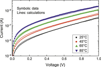
where q is the electron charge, A the cross-section area, N T the concentration of localized states, Δz the distance between positively charged traps, τ0 the pre-exponential time for thermal excitation, kT the thermal energy, and F the electric field. Figure 2 shows measured (symbols) and calculated (lines) current-voltage (I–V) curves for increasing temperatures according to Equation 1.Reference Ielmini and Zhang13 The analytical model accounts for the exponential increase of the current at relatively large voltages and for the voltage dependence of the activation energy for transport, resulting from the field-induced barrier lowering, which is typical of the PF model.Reference Ielmini and Zhang13 Due to the large concentration of localized states, the Fermi level is pinned around midgap, resulting in a large activation energy and a correspondingly high resistance of the amorphous chalcogenide phase. The crystalline phase behaves instead as a doped semiconductor (p-type in the Ge2Sb2Te5 case) with weak temperature activation. The different E F0 positions in the crystalline and amorphous phases explain the large resistance window in PCM between the two chalcogenide phases.
Measured and calculated I–V curves for a phase change memory device in the amorphous state for increasing T. Calculations using Equation 1 are also shown. Reprinted with permission from Reference Reference Ielmini and Zhang13. ©2007, American Institute of Physics.

Transport properties in the crystalline and amorphous chalcogenide phases differ not only by the conduction behavior, but most notably by the previously mentioned threshold switching in the amorphous chalcogenide phase. Threshold switching can be viewed as a reversible electrical breakdown, where conductivity suddenly increases as a threshold voltage V T is reached, resulting in negative differential resistance (NDR) behavior.Reference Ovshinsky1 Threshold switching has been attributed to a variety of physical mechanisms and models, including impact ionization,Reference Adler, Shur, Silver and Ovshinsky14 polaron instability,Reference Emin15 field-induced nucleation,Reference Karpov, Kryukov, Savransky and Karpov16 and structural/carrier heating.Reference Ielmini17
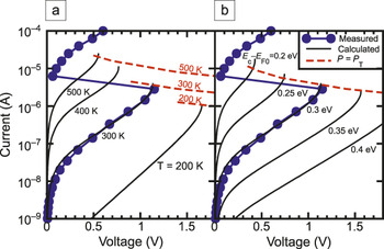
Figure 3 shows the measured and calculated I–V characteristics, including threshold switching. Calculations were obtained from a model for carrier heating at high fields in PF transport.Reference Ielmini17 In this model, the electron distribution is shifted to higher energies due to the high electric field, enhancing the conductivity and yielding the consequent NDR. According to this switching model, the condition for threshold switching is a temperature-dependent constant power P = P T. Calculations by the model are shown for increasing T (Figure 3a) and increasing activation energy E C–E F0 in Equation 1 (Figure 3b). The threshold point, which marks the onset of the NDR regime, obeys the constant-power formula in both figures. The calculated threshold voltage V T decreases for increasing T (Figure 3a) and for decreasing E C–E F0 (Figure 3b), in agreement with literature data.Reference Lee, Jeong, Jeong, Zhe, Park, Ahn and Cheong18
Measured and calculated I–V curves for a phase change memory device in the amorphous state, showing conduction and switching for (a) increasing T and (b) increasing activation energy. Reprinted with permission from Reference Reference Ielmini17. ©2008, American Physical Society.

To evaluate the viability of PCM technology, one of the most important questions is how materials properties change with size and at which spatial dimensions these materials cease to have the required phase change and other electrical and physical properties. Numerous scaling studies on phase change thin films, nanowires, nanoparticles, and ultra-scaled PCM devices have shown very favorable scaling behavior. Many materials properties that are important for the functionality of a PCM device change in a favorable manner. For example, the melting temperature that determines the required RESET current is reduced as dimensions shrink,Reference Raoux, Shelby, Jordan-Sweet, Munoz, Salinga, Chen, Shih, Lai and Lee19 while the crystallization temperature is increased,Reference Caldwell, Raoux, Wang, Wong and Milliron20 leading to better data retention. In other cases, however, a reduction in activation energy of crystallization and thus a deterioration of data retention was reported.Reference Lee, Jung and Agarwal21 This might depend on the actual phase change materials and interfaces. The size limit for a thin film or nanoparticle where at least some phase change materials have been shown to still exist in the amorphous and crystalline states is about 2 nm,Reference Caldwell, Raoux, Wang, Wong and Milliron20 which is quite remarkable because this length corresponds to three times the lattice constant of a typical phase change material. Scaling is also favorable, as it reduces the required currents to switch the devices and reduces the crystallization timesReference Bruns, Merkelbach, Schlockerman, Salinga, Wuttig, Happ, Philipp and Kund3 to values of about 1 ns for advanced prototype PCM devices, making this technology a potential contender for dynamic random-access memory (DRAM) replacement.
Prototype phase change memory fabrication and testing
Many phase change material properties can be studied on blanket films, but the ultimate test of a newly developed material is its performance in a PCM device. One reason for this is that certain properties such as threshold voltage, cyclability, and data retention can only be measured in actual devices; the second reason is that melt-quenched amorphous phase change material, which is the relevant amorphous phase in technological applications, can have very different properties from as-deposited amorphous material.
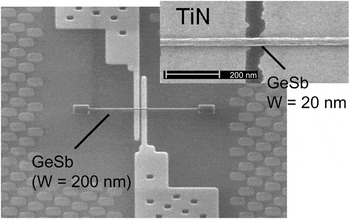
The most aggressively scaled prototype devices made of phase change materials are either pore devices with very small pore diametersReference Bruns, Merkelbach, Schlockerman, Salinga, Wuttig, Happ, Philipp and Kund3 or linear devices fabricated by lithography or made from phase change nanowires.Reference Lee, Jung and Agarwal21, Reference Chen, Rettner, Raoux, Burr, Chen, Shelby, Salinga, Risk, Happ, McClelland, Breitwisch, Schrott, Philipp, Lee, Cheek, Nirschl, Lamorey, Chen, Joseph, Zaidi, Yee, Lung, Bergmann and Lam22 The dimensions of these very small devices are in the few nm to few tens of nm range. Often, scaling is achieved by controlling the film thickness, which is more easily controlled than lithographically fabricated dimensions, as one way to define one of the dimensions of the switching volume.Reference Chen, Rettner, Raoux, Burr, Chen, Shelby, Salinga, Risk, Happ, McClelland, Breitwisch, Schrott, Philipp, Lee, Cheek, Nirschl, Lamorey, Chen, Joseph, Zaidi, Yee, Lung, Bergmann and Lam22Figure 4 shows a particularly small phase change bridge device with a cross-section of 3 nm × 20 nm, to which this fabrication principle was precisely applied controlling one dimension of the phase change material (3 nm) via controlling the film thickness. Small switching volumes were also achieved on nanowire devices, in which material was removed from a portion of the nanowire by a transmission electron microscope (TEM) beam or focused ion beam. This “notch” around the diameter of the nanowire led to a concentration of current and heat at this specific location and defined the switching area of the wire when current pulses were applied. It thus allowed for the detailed study of the phase change material in the SET, fully RESET, and various intermediate states.Reference Jung, Nam and Agarwal23
Plane view scanning electron microscope image of a fabricated bridge device. A closer view of a smaller device is shown in the inset. Reprinted with permission from Reference Reference Chen, Rettner, Raoux, Burr, Chen, Shelby, Salinga, Risk, Happ, McClelland, Breitwisch, Schrott, Philipp, Lee, Cheek, Nirschl, Lamorey, Chen, Joseph, Zaidi, Yee, Lung, Bergmann and Lam22. ©2006, IEEE.

An important parameter for PCM devices is the RESET current because it is the power-limiting factor. Currently, the size of the PCM cell is typically determined by the size of the access device, which delivers the current pulses, not by the memory device. A reduction in RESET current will lead to a reduction in access device size and thus an increase in storage density. The RESET current can be reduced in various ways, including modification of the phase change material, reduction in the size of the switched volume by reduction of the electrode contact area, or a combination of these methods. Measurements clearly show that RESET currents can be effectively reduced by scaling.Reference Chen, Rettner, Raoux, Burr, Chen, Shelby, Salinga, Risk, Happ, McClelland, Breitwisch, Schrott, Philipp, Lee, Cheek, Nirschl, Lamorey, Chen, Joseph, Zaidi, Yee, Lung, Bergmann and Lam22 Another important parameter is the SET (crystallization) time, because it is the data-rate limiting factor. In this case as well, it has been shown that scaling leads to much improved performance, and switching times on the scale of 1 ns have been achieved with very small devices.Reference Bruns, Merkelbach, Schlockerman, Salinga, Wuttig, Happ, Philipp and Kund3
Large scale phase change memory device integration
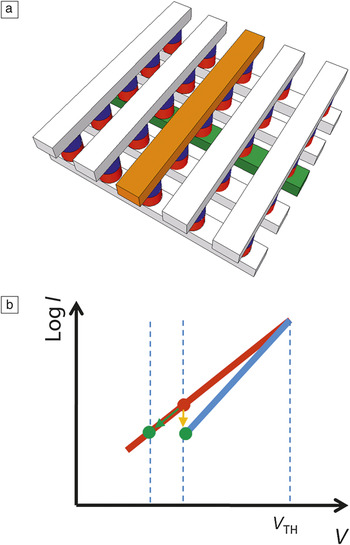
While various PCM memory cells have been proposed and studied in recent years, only few cell designs have been integrated to manufacture large scale memory arrays, up to 1 gigabyte, for 180 nm,Reference Bedeschi, Bez, Boffino, Bonizzoni, Buda, Casagrande, Costa, Ferraro, Gastaldi, Khouri, Ottogalli, Pellizzer, Pirovano, Resta, Torelli and Tosi24 90 nm,Reference Oh, Park, Lim, Lim, Oh, Kim, Shin, Park, Song, Ryoo, Lim, Park, Kim, Kim, Yu, Yeung, Jeong, Kong, Kang, Koh, Jeong, Jeong and Kim25 and 45 nmReference Servalli26 technology nodes. To fabricate large scale memory arrays, the memory cell area, as well as the number of critical masks, becomes a key consideration in terms of cost, in addition to cell efficiency (performance). Also, a large memory array requires a selector device built in series with each memory element to eliminate parasitic currents through the cells in the low resistance state, which are in parallel to the selected cell. Selector devices for arrays reported in References Reference Bedeschi, Bez, Boffino, Bonizzoni, Buda, Casagrande, Costa, Ferraro, Gastaldi, Khouri, Ottogalli, Pellizzer, Pirovano, Resta, Torelli and Tosi24–Reference Servalli26 include metal oxide semiconductor field-effect transistors (MOSFETs) or diodes made in the front end of the complementary metal oxide semiconductor (CMOS) process. Since these selectors use single crystal silicon, such memory arrays cannot be built as stackable memory to allow further increase in memory density. Taking into account that PCM cells are fabricated in CMOS backend, it is possible to consider stackable PCM memory. As seen in Figure 5, each memory layer contains a cross-point array of metal bitlines and orthogonal metal wordlines, with a memory element in series with a thin film selector located at each cross-point.
(a) Cross-point array configuration where memory and selector elements (red and blue) are fabricated in series at each cross-point of a bitline and a wordline. A memory cell is selected by appropriate biases applied to selected wordline (green) and bitline (orange) and to deselected wordlines and bitlines (white). (b) Sub-threshold log (I) versus V characteristics of a selector illustrating different ways to reduce array leakage by change in subthreshold slope (yellow arrow) or by reducing bias (green arrow).

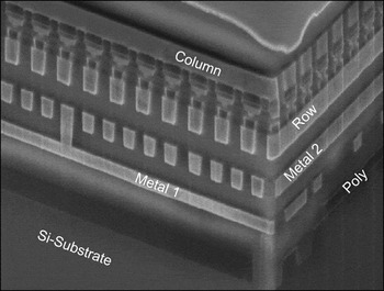
The key requirements to design a selector are low leakage current to enable large arrays, and high on-current capability, to provide sufficient programming current to the memory cell. On-current scaling with device size, endurance, and even processing temperature also need to be considered. Polycrystalline Si p-n junction diode,Reference Sasago, Kinoshita, Morikawa, Kurotsuchi, Hanzawa, Mine, Shima, Fujisaki, Kume, Moriya, Takaura and Torii27 oxide-based p-n junction diode,Reference Lee, Park, Kang, Ahn, Lee, Kim, Xianyu, Stefanovich, Lee, Chung, Kim, Lee, Park and Yoo28 oxide-based Schottky diode,Reference Tallarida, Huby, Kutrzeba-Kotowska, Spiga, Arcari, Csaba, Lugli, Redaelli and Bez29 mixed ionic-electronic conductor (MIEC),Reference Gopalakrishnan, Shenoy, Rettner, Virwani, Bethune, Shelby, Burr, Kellock, King, Nguyen, Bowers, Jurich, Jackson, Friz, Topuria, Rice and Kurdi30 and Ovonic threshold switch (OTS)Reference Kau, Tang, Karpov, Dodge, Klehn, Kalb, Strand, Diaz, Leung, Wu, Lee, Langtry, Chang, Papagianni, Lee, Hirst, Erra, Flores, Righos, Castro and Spadini31 devices have been evaluated as selectors. No device scores the best in all categories; however, OTS shows a great deal of promise. It was recently integrated with a PCM element to form 64 Mb arrays;Reference Kau, Tang, Karpov, Dodge, Klehn, Kalb, Strand, Diaz, Leung, Wu, Lee, Langtry, Chang, Papagianni, Lee, Hirst, Erra, Flores, Righos, Castro and Spadini31 this combination is known as PCMS (Figure 6). As illustrated in Figure 6, the PCMS cell for this prototype array consists of two devices, PCM and OTS, in series, interlinked by a middle electrode.
Phase change memory cross-point array with Ovonic threshold switch selector, sandwiched between row and column metal layers in the backend of the process, and integrated with complementary metal oxide semiconductor technology. Reprinted with permission from Reference Reference Kau, Tang, Karpov, Dodge, Klehn, Kalb, Strand, Diaz, Leung, Wu, Lee, Langtry, Chang, Papagianni, Lee, Hirst, Erra, Flores, Righos, Castro and Spadini31. ©2009, IEEE.

Important requirements for cross-point array operation are that while the selected cell is read or written, the deselected cells are kept in the off-state to ensure that they are not disturbed, and their off-current does not interfere with the sensing of the current from the selected cell. To address these requirements, a proper biasing scheme must be devised for both read and write operations. For example, OTS off-state leakage current on the selected bitline can be reduced by lowering the bias for the deselected cells. Alternatively, to accomplish the same result, an OTS material can be chosen with a suppressed sub-threshold conduction and a steeper sub-threshold slope, as illustrated in Figure 5b.
In addition to sub-threshold conduction,Reference Simon, Nardone, Kostylev, Karpov and Karpov32 threshold switching, the different features it exhibits, and its dependence on ambient temperature, time, device geometry, and material parameters,Reference Karpov, Kryukov, Savransky and Karpov16, Reference Karpov, Mitra, Kau, Spadini, Kryukov and Karpov33–Reference Karpov, Kau, Spadini and Karpov35 are all key to PCMS technology development.
Summary and outlook
Rewritable optical storage technology based on phase change materials has been a great technological success story that initiated large research and development efforts toward the development of solid-state memory based on these materials. The recent years have seen great progress in the application of phase change materials in phase change memory (PCM), and products are already on the market. In parallel, materials research will lead to a better understanding of the relationship between structure and properties. Many problems are still not solved, and we are far away from the ideal situation when one can design a novel phase change material based on first principles and predict optical and electrical properties. Nevertheless, in particular due to its excellent scaling properties, PCM can be expected to play an increasing role in the memory landscape of the future.