Introduction
Wide-Bandgap (WBG) semiconductor devices are promising candidates for next-generation power electronic converters.[Reference Galazka1–Reference Eum, Oyama and Otake9] Power electronic applications range from on-chip power converters to very high voltage rectifiers for electric power transmission lines.[Reference Bayraktaroglu2, Reference Higashiwaki and Jessen3, Reference Cheng7–Reference Eum, Oyama and Otake9] The potential application space includes power generation (solar and wind), power distribution and conversion in electricity grids, electric vehicles, server farms, and charging infrastructure.[Reference Bayraktaroglu2, Reference Cheng7–Reference Eum, Oyama and Otake9] High-voltage switching transistors used in these applications are required to have small ON resistance while providing very high blocking voltages in the OFF state. There are already kV-range power switches today, based on SiC and GaN.[Reference Cheng7–Reference Eum, Oyama and Otake9] These include a 1200 V direct-driven SiC Junction Field Effect Transistor power switch[Reference Singh and Sundaresan8] and reliable GaN Metal Oxide–Semiconductor (MOS) Heterostructure Field Effect Transistors (HFETs).[Reference Eum, Oyama and Otake9]
The β-polymorph of Ga2O3 has an even larger power figure-of-merit than these two materials and is available in large area bulk and epitaxial layer form.[Reference Galazka1–Reference Higashiwaki and Jessen3, Reference Pearton, Yang, Carey, Ren, Kim, Tadjer and Mastro6] The potential target for the Ga2O3 devices, if the material quality continues to improve and appropriate device processing techniques are developed, will be in the 100s of kV–MV range.[Reference Bayraktaroglu2] However, the prohibitive cost and limited variety of device types currently possible are still the main constraints before Ga2O3 will be widely used in power electronics applications. One possible solution to mitigate these issues is hybrid switches: a combination of Si metal oxide semiconductor field effect transistors (MOSFETs) and WBG devices such as Ga2O3 rectifiers or GaN High Electron Mobility Transistors (HEMTs). In the latter case, 400 V/80A full bridge prototypes have been developed that show the ability to continuously turn off 400 V/80A@100 kHz and 400 V/40A@300 kHz with only one GaN device paralleled to two commercial Si MOSFETs.[Reference Bayraktaroglu2] Ga2O3 would have an even larger voltage capability.
High-power (~50 kW) is also required for fast wireless charging systems (WCS) in transportation applications.[Reference Bayraktaroglu2, Reference Pearton, Yang, Carey, Ren, Kim, Tadjer and Mastro6, Reference Cheng7] In this application, the operating frequency of the WCS determines the size and configuration of the pad, the range of charging distance, and the quality factor of the resonant tank. Low power systems in the range 3.7–11.0 kW have been standardized to operate at 85 kHz. However, higher-power systems at 10–22 kHz reduce the switching loss in the inverter as well as conductive and magnetic losses in the power pad. At these frequencies, higher current is required to transfer the same power levels. Moreover, the mutual inductance is lower in case of dynamic wireless charging. SiC-based inverters are being developed for wireless vehicular charging applications and Ga2O3 is a possible candidate due to the promising rectifier results reported to date.[Reference Bayraktaroglu2, Reference Higashiwaki and Jessen3, Reference Pearton, Yang, Carey, Ren, Kim, Tadjer and Mastro6]
Relevant properties and limitations of Ga2O3
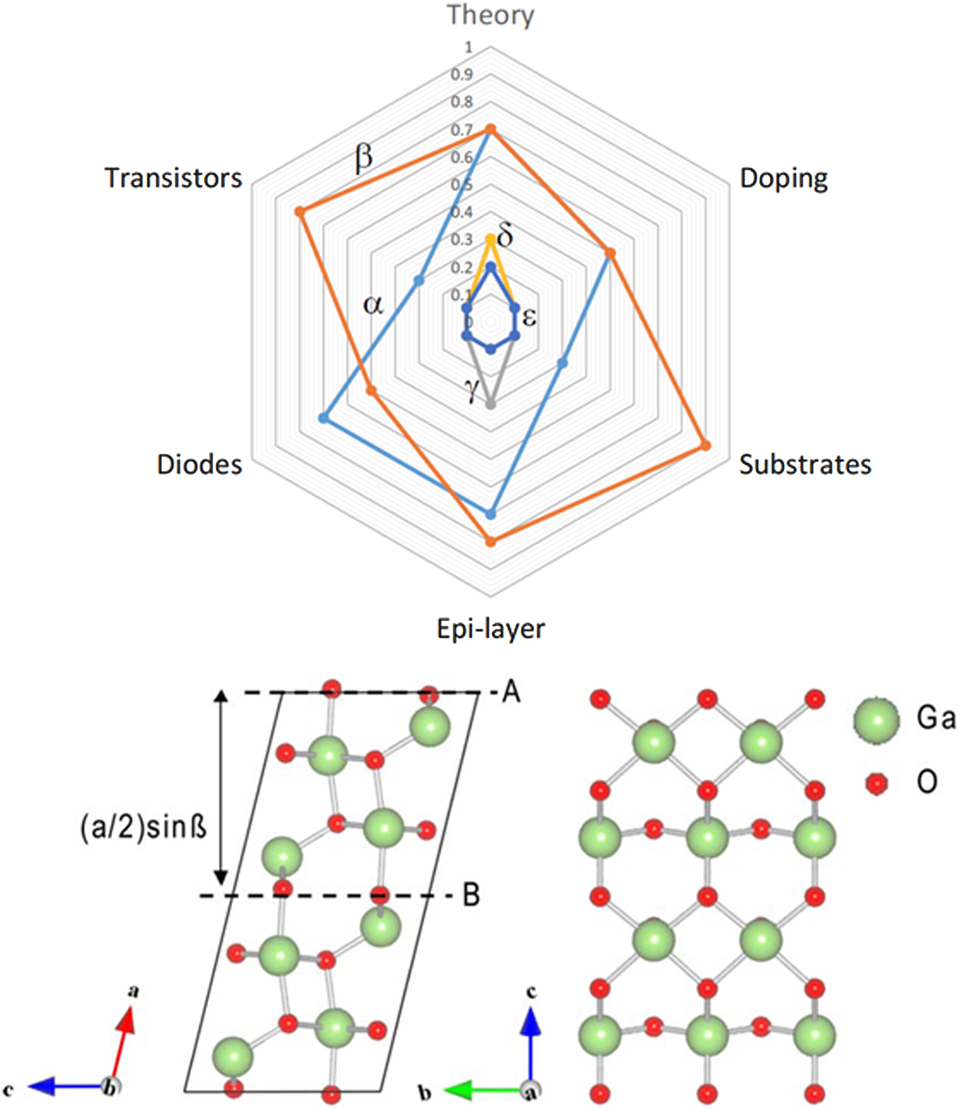
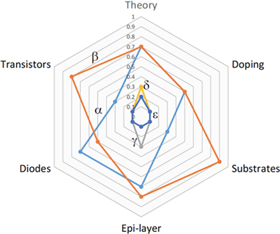
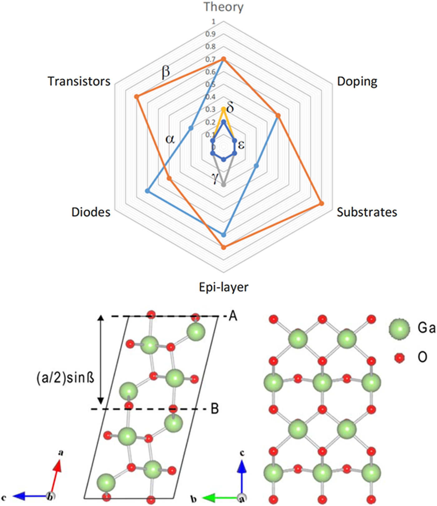
While there are a number of polymorphs of Ga2O3, the most stable and widely studied is monoclinic β-Ga2O3.[Reference Galazka1, Reference Varley, Janotti, Franchini and Van de Walle10–Reference Higashiwaki, Sasaki, Kuramata, Masui and Yamakoshi13] The corundum structure α-Ga2O3 has a wider bandgap but is more difficult to stabilize. Figure 1 shows that the β-polymorph is the most developed in terms of devices, substrate, and epi layer availability.[Reference Bayraktaroglu2] Cross-sections of the β-polymorph crystal structure are shown at the bottom of the figure. For power switching applications, there are several drawbacks of β-Ga2O3, including its low thermal conductivity and the absence of p-type doping capability.[Reference Galazka1–Reference Tadjer, Mahadik, Wheeler, Glaser, Ruppalt and Koehler4, Reference Pearton, Yang, Carey, Ren, Kim, Tadjer and Mastro6, Reference Varley, Janotti, Franchini and Van de Walle10] The use of minority carrier assisted turn-on mechanisms are an intrinsic part of current power electronics. Ga2O3-based power devices would benefit from the availability of minority carrier so that PIN type diodes and IGBT (insulated gate bipolar transistor) type transistors can be fabricated. These devices preserve the high voltage blocking capacity while lowering the on-state resistance. Such devices exceed the theoretical limits of unipolar devices. As a consequence of its doping limitations, all Ga2O3 devices are majority carrier type.[Reference Galazka1–Reference Pearton, Yang, Carey, Ren, Kim, Tadjer and Mastro6] The two-terminal devices reported include rectifiers, UV solar-blind photoconductors, and photodetectors.[Reference Galazka1–Reference Pearton, Yang, Carey, Ren, Kim, Tadjer and Mastro6, Reference Higashiwaki, Sasaki, Kuramata, Masui and Yamakoshi13–Reference Tadjer, Mahadik, Freitas, Glaser, Koehler, Luna, Feigelson, Hobart, Kub and Kuramata15] Three-terminal devices reported include MESFETs and MOSFETs, mostly operating in depletion mode. At this stage, the theoretical critical field of Ga2O3 of~8 MV/c (extrapolated from other materials), has not been achieved experimentally, with values in the range 1.5–4.4 MV.cm−1.[Reference Tadjer, Mahadik, Freitas, Glaser, Koehler, Luna, Feigelson, Hobart, Kub and Kuramata15]
(top) Qualitative representation of the technology development status of the different polymorphs of Ga2O3 and (bottom left) unit cell along (010) direction and (bottom right) normal to the (100) surface of β-Ga2O3.
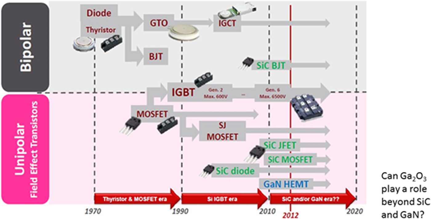
The absence of a p-type doping capability is due to the flatness of the valence band, which leads holes to effectively self-trap, giving rise to localize polarons.[Reference Varley, Janotti, Franchini and Van de Walle10, Reference Watahiki, Yuda, Furukawa, Yamamuka, Takiguchi and Miyajima14–Reference Higashiwaki, Sasaki, Wong, Kamimura, Krishnamurthy, Kuramata, Masui and Yamakoshi19] There have been reports of p-type conductivity from ionized Ga vacancies at elevated temperature,[Reference Chikoidze, Fellous, Perez-Tomas, Sauthier, Tchelidze, Ton-That, Huynh, Phillips, Russell, Jennings, Berini, Jomard and Dumont20] but extrinsic acceptors are not electrically active at room temperature.[Reference Kyrtsos, Matsubara and Bellotti21] Electronic devices are broadly classified as bipolar (minority carrier) or unipolar (majority carrier). Majority carrier devices usually switch faster and include Schottky diode rectifiers and MOSFETs. Minority carrier devices usually have better on-state performance and include p-i-n diode rectifiers, bipolar junction transistors (BJTs), IGBTs, and thyristors.[Reference Bayraktaroglu2, Reference Higashiwaki and Jessen3] These latter two play a large role in Si power electronics but will be challenging to achieve in Ga2O3 because of the lack of p-type doping. The current approach is to employ p-type semiconductors such as SiC, NiO, Cu2O, CuI, or diamond to make vertical p-n heterojunctions.[Reference Watahiki, Yuda, Furukawa, Yamamuka, Takiguchi and Miyajima14–Reference Nakagomi, Hiratsuka, Kakuda and Kokubun17] Figure 2 shows the evolution of Si power electronics and where SiC and GaN have begun to have an impact.
Evolution of Si power electronics based on both majority and minority carrier devices and the beginning of the availability of SiC and GaN devices to provide higher performance.
It is not clear that multiple junction devices in Ga2O3 can be made successfully using these other p-type materials, since even single junction demonstrations have shown significant limitations.[Reference Tadjer, Mahadik, Freitas, Glaser, Koehler, Luna, Feigelson, Hobart, Kub and Kuramata15] The quality of the junctions must be very high in order to achieve acceptable performance in devices such as IGBTs and thyristors. These are three terminal devices with a controlling “gate” terminal but utilize different principles of operation. The thyristor has four alternating semiconductor layers (e.g., p-n-p-n), i.e., three p-n junctions and is basically a coupled pair of pnp and npn transistors. The outermost P- and N-type layers are the anode and cathode respectively, with the inner P-type layer acting as the “gate”. It has three modes of operation, namely reverse blocking mode, forward blocking mode, and forward conducting mode. Once the gate is triggered, the thyristor is in forward conducting mode and keeps conducting until the forward current becomes less than the threshold holding current. Thyristors are mainly used in control of alternating currents. The IGBT has three terminals (emitter, collector, and gate). It can handle high powers at fast switching speed and has the combined features of both MOSFET and BJT. It is gate driven, like a MOSFET, and has current-voltage characteristics like BJTs. Therefore, it has the advantages of both high current handling capability and ease of control. Si IGBT modules can handle kilowatts of power, with much larger capabilities for the wider gap materials if they have appropriate carrier lifetime and junction capability. Currently, the single p-n heterojunctions involving Ga2O3 do not generally indicate minority carrier injection at low bias, indicating that a true p-n junction is not formed.
An important parameter in bipolar power devices is the minority carrier lifetime. Indirect semiconductors have a longer minority carrier lifetime compared to direct bandgap semiconductors. Lifetimes of 215 ps were reported for nonequilibrium holes created by e-beam excitation of n-type Ga2O3.[Reference Lee, Flitsiyan, Chernyak, Yang, Ren, Pearton, Meyler and Salzman18]
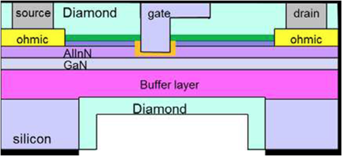
One limitation to Ga2O3 material for power electronics is its low thermal conductivity at 11–27 W/mK, particularly when contrasted to the thermal conductivity of Si (130 W/mK), SiC (360–490 W/mK), and GaN (150–200 W/mK).[Reference Galazka1–Reference Higashiwaki and Jessen3] This means that thermal management approaches will be critical in power applications and these include top and bottom heat sinks and microfluidic channel to bring cooling fluid to the active region of the device. One approach for mitigating the low thermal conductivity of Ga2O3 is by integrating diamond, AlN, or Cu as a high thermal conductivity heat spreader.[Reference Tadjer, Anderson, Hobart, Feygelson, Caldwell, Eddy, Kub, Butler, Pate and Melngailis22–Reference Meyer, Feygelson, Anderson, Roussos, Tadjer, Downey, Katzer, Pate, Ancona, Koehler, Hobart and Eddy24] Integration of Ga2O3 with diamond, which has nearly an order of magnitude higher thermal conductivity than Cu, is the most attractive option for high power Ga2O3 devices.[Reference Tadjer, Anderson, Hobart, Feygelson, Caldwell, Eddy, Kub, Butler, Pate and Melngailis22–Reference Meyer, Feygelson, Anderson, Roussos, Tadjer, Downey, Katzer, Pate, Ancona, Koehler, Hobart and Eddy24] However, diamond and Ga2O3 are incompatible from a growth standpoint, as the growth atmosphere of one is detrimental to the other (H-plasma for Ga2O3, O-plasma for diamond). Development of approaches for the growth of Ga2O3 on single-crystal diamond, as well as CVD nanocrystalline diamond on both Ga2O3 substrates and devices is an area of need. The existing embedded thermal management approaches developed for GaN, where cooling is built into the chip, substrate, and/or package to directly cool the heat generation sites using high-thermal-conductivity synthetic diamond material either to line microfluidic channels or to form the substrate of the RF chips,[Reference Bayraktaroglu2, Reference Pearton, Yang, Carey, Ren, Kim, Tadjer and Mastro6] is something that could be quickly applied to Ga2O3. Groups at the Naval Research Laboratories have demonstrated the integration of nanocrystalline diamond on both the front-side and backside of GaN HEMTs to effectively remove the heat from its source (drain edge of the gate) to heat sinks.[Reference Tadjer, Anderson, Hobart, Feygelson, Caldwell, Eddy, Kub, Butler, Pate and Melngailis22–Reference Meyer, Feygelson, Anderson, Roussos, Tadjer, Downey, Katzer, Pate, Ancona, Koehler, Hobart and Eddy24] A schematic is shown in Fig. 3. These devices have achieved 20% (25–50 °C) reductions in device operating temperature while enhancing DC and RF performance.[Reference Tadjer, Anderson, Hobart, Feygelson, Caldwell, Eddy, Kub, Butler, Pate and Melngailis22–Reference Meyer, Feygelson, Anderson, Roussos, Tadjer, Downey, Katzer, Pate, Ancona, Koehler, Hobart and Eddy24]
Schematic cross-section of GaN power transistor with integrated nanocrystalline diamond coatings for improved heat dissipation.

Given the basic properties of Ga2O3, where is it likely to have an impact? The status of p-n heterojunctions is too crude for practical applications. For rf applications, it is hard to see where Ga2O3 brings advantages, although gate-all-around FinFETs can operate in accumulation mode in the on state.[Reference Chabak, Moser, Green, Walker, Tetlak, Heller, Crespo, Fitch, McCandless, Leedy, Baldini, Wagner, Galazka, Li and Jessen25] Additionally, for lateral devices, the (AlxGa1−x)2O3/Ga2O3 heterostructure has been recently demonstrated using modulation doping of the barrier layer,[Reference Ahmadi, Koksaldi, Zheng, Mates, Oshima, Mishra and Speck26–Reference Wakabayashi, Hattori, Yoshimatsu, Horiba, Kumigashira and Ohtomo30] as β-Ga2O3 is nonpolar. There needs to be a major breakthrough, such as a >5 kV transistor or Ga2O3 on diamond HFETs. The future of Ga2O3 depends on its ability to find a profitable, sustainable commercial application. Solar-blind, ultra-violet photodetectors are a niche application (the 4.7–4.9 eV bandgap of Ga2O3 renders it naturally solar-blind). The vertical Schottky barrier diodes matching the recovery characteristics of SiC SBDs have been demonstrated but offer no performance advantage at this time.[Reference Takatsuka, Sasaki, Wakimoto, Thieu, Koishikawa, Arima, Hirabayashi, Inokuchi, Fukumitsu, Kuramata and Yamakoshi31, Reference Yang, Ren, Chen, Liao, Chang, Lin, Tadjer, Pearton and Kuramata32] However, continued performance improvements would be a useful addition to the power electronics market as a fast, cheap, robust, low-loss switch.
Processing needs
Vertical devices need field termination to avoid electric field crowding. For SiC and GaN, p-type termination regions such as guard rings and junction termination extensions, patterned selectively using either regrowth or implantation, have been vital. Again, this is very difficult to implement in Ga2O3 and simpler field termination must be employed.
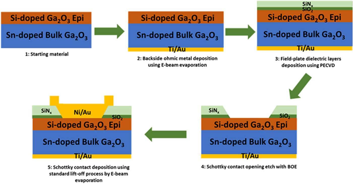
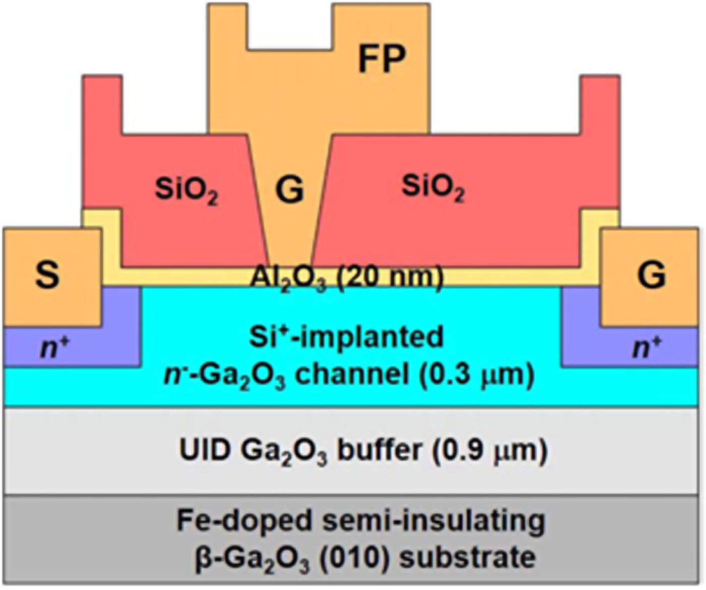
Let us examine the process sequence for a typical vertical geometry rectifier, shown in Fig. 4. This is relatively straightforward, involving a full area backside Ohmic contact, top Schottky contact, and overlap of this contact onto a dielectric layer. For a three terminal device, such as the MOSFET shown in Fig. 5, a simplified sequence involves the following steps:
(i) Device Isolation––the active region is defined by mesa etching using low damage Cl2/BCl3-based inductively coupled plasma etching or by ion implantation to create highly resistive regions.
(ii) Ohmic contact formation—a typical Ohmic on n-Ga2O3 is a Ti/Pt/Au metal stack deposited by e-beam evaporated and annealed in O2
(iii) Gate recess etching—threshold voltage control by recess dry etching
(iv) Gate oxide deposition—Al2O3 or SiO2 gate oxide deposited by ALD
(v) Gate electrode metallization—typically Ni/Au metal stack e-beam evaporated for the gate formation
(vi) O2 ambient post-metallization annealing—post-metallization annealing in O2 ambient to improve the interface quality of the Al2O3/Ga2O3 or SiO2/Ga2O3.
Schematic of processing sequence for Ga2O3 power rectifier, showing edge termination, thermally stable Schottky, and low resistance Ohmic.

Schematic of trench MOS Schottky diode. Reprinted with permission from ref. Reference Wong, Sasaki, Kuramata, Yamakoshi and Higashiwaki5 (IEEE, 2018).

Most of these same steps are generic to any two or three terminal Ga2O3 device. In addition, while we show a Ga2O3 channel MOSFET in Fig. 5, the use of (AlxGa1−x)2O3 two-dimensional electron gas (2DEG) channels allows high carrier density and mobility (high on-state driving current) and fast switching speed.[Reference Ahmadi, Koksaldi, Zheng, Mates, Oshima, Mishra and Speck26–Reference Wakabayashi, Hattori, Yoshimatsu, Horiba, Kumigashira and Ohtomo30]
All of the devices benefit from the addition of field plates to tailor the electric field profile, although multiple field plates have yet to be implemented and this might improve the dynamic on-resistance in FETs. Current collapse phenomena have been observed in MOSFETs but not studied to the extent they have in AlGaN/GaN HEMTs. This can be caused by reversible trapping into surface defects, AlGaO barrier bulk traps, interfacial traps at the AlGaO/GaO interface, and buffer traps. In recessed gate MOS configurations, there can be additional fixed/interface charges and plasma-induced recess damage. Again, the addition of field plates can reduce the current collapse and increase breakdown voltage by suppressed electric field reduce the probability of electron injection from the gate.
Contacts
Ohmic contacts
It is always challenging to make low resistance Ohmic contacts to wide bandgap semiconductors and generally some form of local doping enhancement by ion implantation,[Reference Sasaki, Higashiwaki, Kuramata, Masui and Yamakoshi12, Reference Zolper33, Reference Wong, Lin, Kuramata, Yamakoshi, Murakami, Masataka and Higashiwaki34] plasma exposure,[Reference Sasaki, Higashiwaki, Kuramata, Masui and Yamakoshi12] or the addition of a low bandgap interlayer (AZO, ITO, InN)[Reference Carey, Yang, Ren, Hays, Pearton, Jang, Kuramata and Kravchenko35, Reference Carey, Yang, Ren, Hays, Pearton, Jang, Kuramata and Kravchenko36] is used. Ion implantation is still relatively unexplored in Ga2O3 in terms of choice of species, doses, and annealing conditions.[Reference Sasaki, Higashiwaki, Kuramata, Masui and Yamakoshi12, Reference Wong, Lin, Kuramata, Yamakoshi, Murakami, Masataka and Higashiwaki34] It is necessary to achieve highly conductive surface layers for Ohmic contacts formation. In this case of ion implantation, this means carrier concentrations of 1019–1020/cm3. Activation annealing has typically been carried out at 900–1000 °C for 30 min, with activation percentages approaching 60%.[Reference Sasaki, Higashiwaki, Kuramata, Masui and Yamakoshi12, Reference Wong, Lin, Kuramata, Yamakoshi, Murakami, Masataka and Higashiwaki34] When annealed in N2, there was no change in surface morphology at temperatures below 1150 °C, however, the addition of hydrogen to the annealing ambient lowered the temperature at which degradation was evident.[Reference Hoshikawa, Ohba, Kobayashi, Yanagisawa, Miyagawa and Nakamura37, Reference Togashi, Nomura, Eguchi, Fukizawa, Goto, Thieu, Murakami, Kumagai, Kuramata and Yamakoshi38] Thermodynamic analysis showed that the dominant reactions are Ga2O3(s) = Ga2O(g) + O2 (g) in N2 and Ga2O3(s) + 2H2(g) = Ga2O(g) + 2H2O (g) in a mixed flow of H2 and N2. A simple expedient is to perform the implant activation anneals in O2 ambient.[Reference Hoshikawa, Ohba, Kobayashi, Yanagisawa, Miyagawa and Nakamura37–Reference Nikolaev, Maslov, Stepanov, Pechnikov, Krymov, Nikitina, Guzilova, Bougrov and Romanov40]
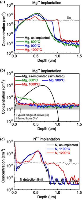
One surprising feature of the few implantation studies to date has been the high diffusivities of some of the implanted species.[Reference Wong, Lin, Kuramata, Yamakoshi, Murakami, Masataka and Higashiwaki34] Secondary Ion Mass Spectrometry (SIMS) depth profiles of Mg and N are shown in Fig. 6.[Reference Wong, Lin, Kuramata, Yamakoshi, Murakami, Masataka and Higashiwaki34] Significant Mg diffusion occurred at T a ≥ 900 °C, with the as-implanted Gaussian Mg profile transformed into box-like with a sharp cutoff tail and a plateau concentration stabilized at the background donor (Sn) concentration.[Reference Wong, Lin, Kuramata, Yamakoshi, Murakami, Masataka and Higashiwaki34] This diffusion was independent of the impurity concentrations or the specific donor species involved. By contrast, implanted N profiles showed limited redistribution at 1200 °C and also stabilized at the background donor (Si) concentration of 2 × 10¹⁷/cm3.
SIMS profiles of Mg or N implants into Ga2O3 before and after annealing at different temperatures. In (a), Mg profiles in heavily Sn-doped substrates before and annealing at 800–1000 °C, (b) Mg profiles in lightly Sn-doped substrates before and after annealing at 800–1000 °C and (c) N and Si profiles in undoped substrates before and after annealing at 1100–1200 °C. [Reprinted with permission from ref. Reference Wong, Lin, Kuramata, Yamakoshi, Murakami, Masataka and Higashiwaki34 (American Institute of Physics, 2018)].

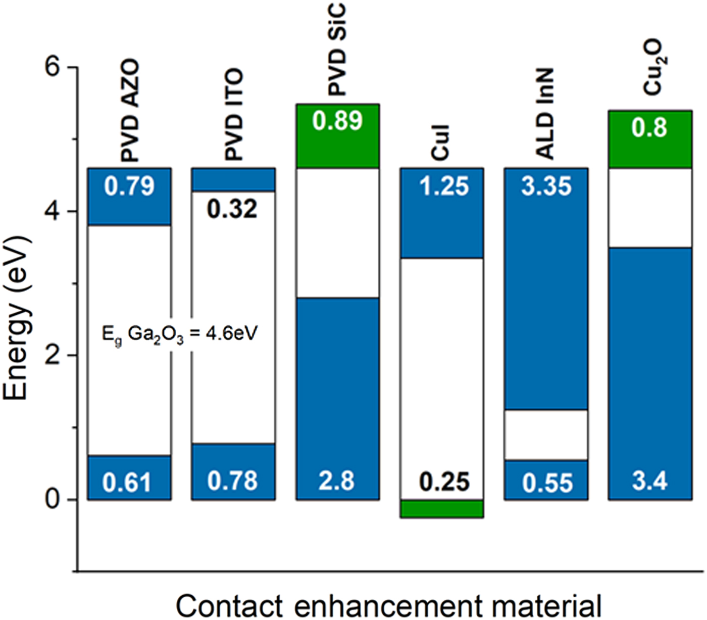
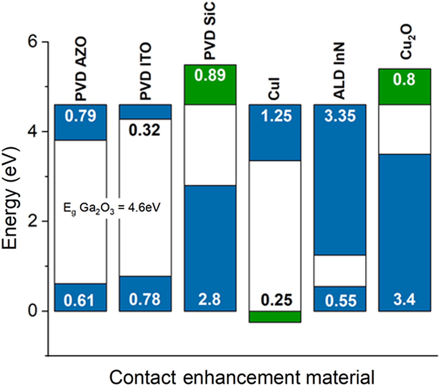
Sasaki et al. reported Ohmic contacts to Ga2O3 using implanted Si to form n+ regions under the contact metal.[Reference Sasaki, Higashiwaki, Kuramata, Masui and Yamakoshi12] The implants were activated by 950 °C rapid-thermal annealing. Ohmic contacts made to these Si-implanted layers using Ti/Au metallization showed a specific contact resistivity of 4.6 × 10⁻⁶/Ω.cm2, using a three-step contact process (BCl3/Ar etch, Ti/Au metal liftoff, 1 min. 450 °C RTA), Other variations employ additional metal layers such as Al, Ni, and Pt in the stack. It is not clear the insertion of these additional metal layers has had a positive impact on the Ohmic contact performance.[Reference Tadjer, Mahadik, Freitas, Glaser, Koehler, Luna, Feigelson, Hobart, Kub and Kuramata15] Carey et al. reported Al-doped ZnO (AZO) interlayers and compared to the Ohmic characteristics to Ti/Au.[Reference Carey, Yang, Ren, Hays, Pearton, Jang, Kuramata and Kravchenko36] For the AZO process, the Ga2O3 was implanted with Si, followed by a 10/20/80 nm thick AZO/Ti/Au stack. The AZO contact exhibited nearly linear I-V characteristics even as-deposited. By comparison, the Ti/Au reference contact did not exhibit linear current-voltage characteristics even after annealing up to 600 °C. The contact resistance of 0.42 Ω·mm (2.8 × 10⁻⁵ Ω/cm2) was reported for annealing at 400–600 °C, demonstrating the AZO/Ga2O3 heterojunction has great potential for Ohmic contacts in Ga2O3 devices. In a separate study, ITO/Ga2O3 contacts were fabricated as well,[Reference Carey, Yang, Ren, Hays, Pearton, Jang, Kuramata and Kravchenko35] with the lowest value for the specific contact resistance of 0.60 Ω·mm (6.3 × 10⁻⁵ Ω/cm2) achieved after 600 °C annealing. Figure 7 shows the band alignments for some potential interfacial layers for reducing contact resistance on Ga2O3.
Band alignments for contact interlayer materials on Ga2O3.
What is needed to further improve contact resistance? The versatility of ion implantation needs to be exploited. For most semiconductors, the implant activation temperature generally follows a two-thirds rule with respect to the melting point.[Reference Zolper33] The melting temperature of Ga2O3 is 1793–1820 °C,[Reference Galazka1, Reference Mu, Jia, Yin, Hu, Li, Wu, Zhang and Tao39, Reference Nikolaev, Maslov, Stepanov, Pechnikov, Krymov, Nikitina, Guzilova, Bougrov and Romanov40] so the 2/3 rule for implant activation annealing suggests temperatures in the range 1150–1250 °C. This is higher than generally employed to date. Annealing conditions consisting of a high temperature for a short duration are desirable for materials containing volatile elements, like oxides. These annealing conditions can give improved electrical properties and restrict surface degradation, dopant redistribution, and mobility degradation. The temperatures required for many wide bandgap semiconductors are beyond the capability of most rapid thermal annealing systems. Ga2O3 decomposes into volatile lower oxides when heated under oxygen deficient atmospheres. The following decomposition reactions take place[Reference Carey, Yang, Ren, Hays, Pearton, Jang, Kuramata and Kravchenko36–Reference Nikolaev, Maslov, Stepanov, Pechnikov, Krymov, Nikitina, Guzilova, Bougrov and Romanov40]:
 $$\eqalign{{\rm G}{\rm a}_2{\rm O}_3\lpar {{\rm l},{\rm} {\rm s}} \rpar & \,\to \,2{\rm GaO}{\rm} \lpar {\rm g} \rpar + 1/2{\rm O}_2\lpar {\rm g} \rpar ,{\rm} 2{\rm GaO}{\rm} \lpar {\rm g} \rpar \cr & \,\to \,{\rm G}{\rm a}_2{\rm O}{\rm} \lpar {\rm g} \rpar + 1/2{\rm O}_2\lpar {\rm g} \rpar ,{\rm} {\rm G}{\rm a}_2{\rm O}{\rm} \lpar {\rm g} \rpar \cr & \,\to \,2{\rm Ga}{\rm} \lpar {\rm g} \rpar + 1/2{\rm O}_2\lpar {\rm g} \rpar}.$$
Thermal decomposition of β-Ga2O3 becomes noticeable at temperatures above 1200 °C. Experiments on annealing at different temperatures and atmospheres showed stability of the (100) surface in O2 to ~1300 °C, in N2 or Ar to ~ 1200 °C, and in the presence of H2 (5% H2 + 95% Ar) to ~600 °C for an annealing time of 10 h.[Reference Mu, Jia, Yin, Hu, Li, Wu, Zhang and Tao39, Reference Nikolaev, Maslov, Stepanov, Pechnikov, Krymov, Nikitina, Guzilova, Bougrov and Romanov40] RTA conditions can extend these stability limits.
Schottky contacts
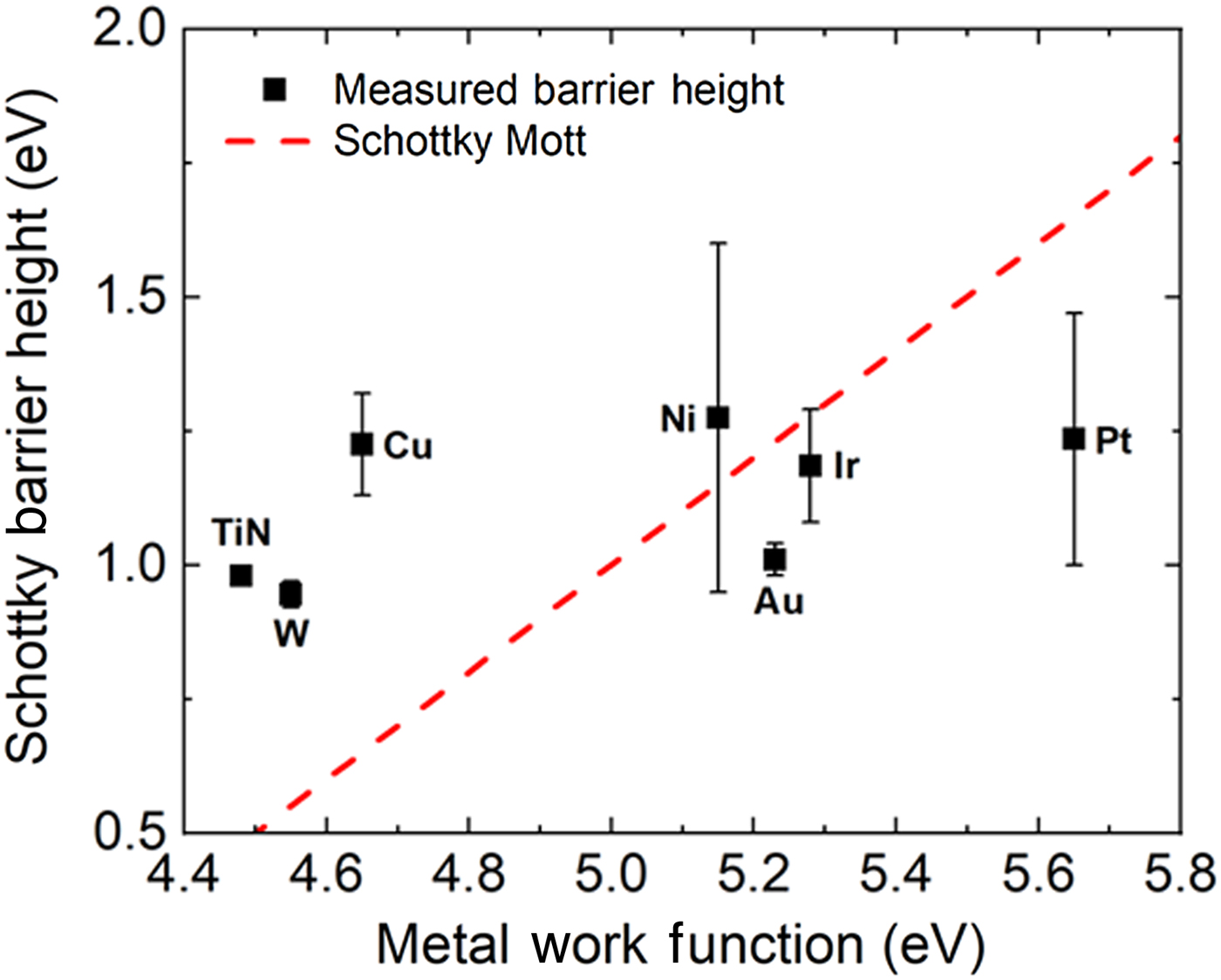
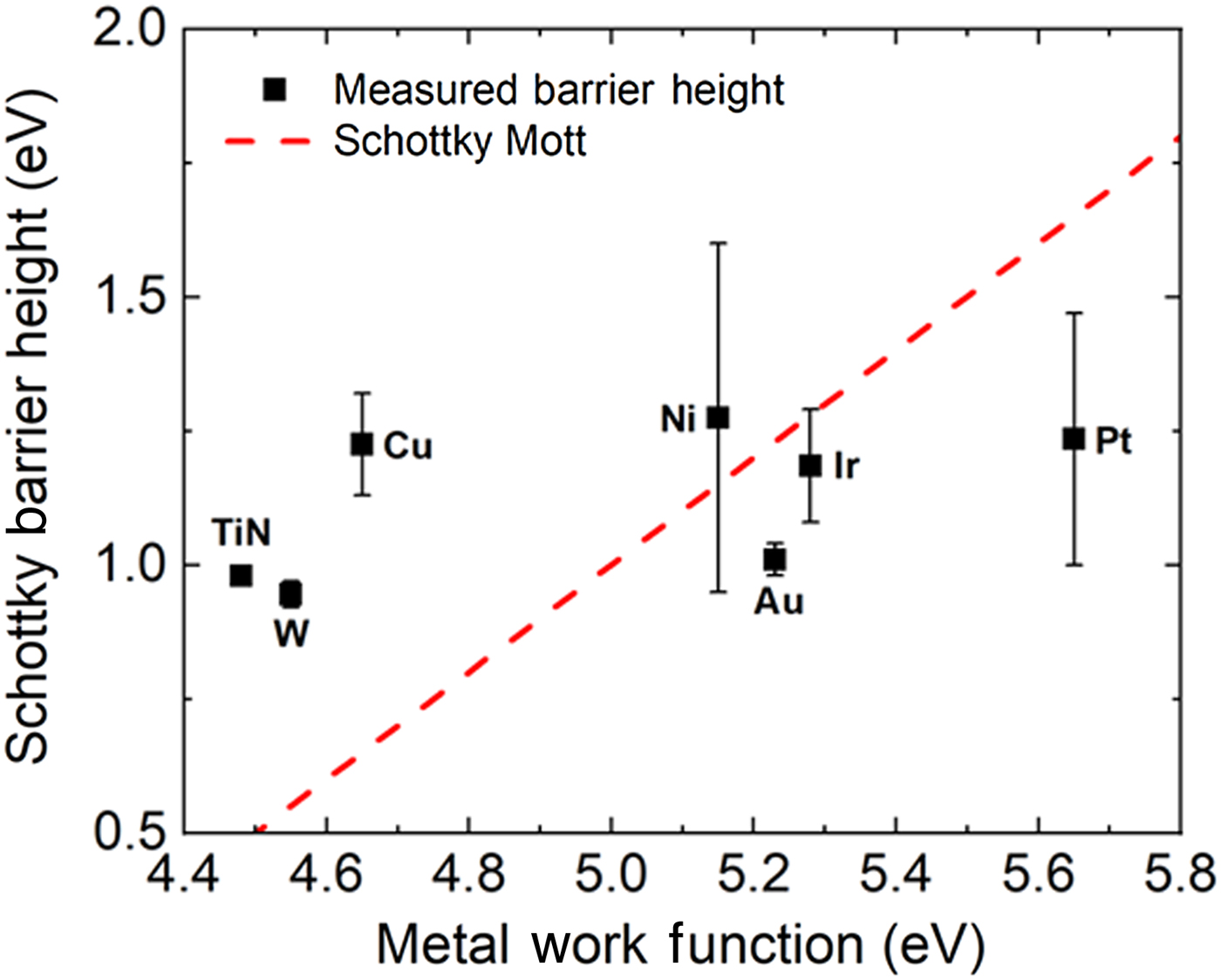
High barrier height, thermally stable (W, WNx, WCx) have yet to be explored for Ga2O3. Currently, high work function metals are typically used as Schottky contacts, with Ni and Pt the most common.[Reference Tadjer, Mahadik, Freitas, Glaser, Koehler, Luna, Feigelson, Hobart, Kub and Kuramata15, Reference Yao, Davis and Porter41–Reference Farzana, Zhang, Paul, Arehart and Ringel50] Prior to deposition, the surface is generally cleaned with organic solvents (acetone-methanol/isopropyl alcohol) usually with ultrasonic agitation and followed with various wet chemical treatments. Yao et al.[Reference Yao, Davis and Porter41] reported HCl + H2O2 produced the highest Schottky barrier heights and lowest series resistances. The effect of the choice of metal on the Schottky behavior is still unclear. Scattered barrier heights with weak correlation to metal work function, as shown in Fig. 8, may indicate that there is at most only a partial Fermi level pinning due to defects and/or surface states, particularly on the (201) surface. Behavior closer to that predicted by the Schottky-Mott model is observed for (010) orientation.[Reference Schottky51–Reference Mott54] Most of the reported Schottky barrier heights on β-Ga2O3 are between ~1.0 and 1.5 eV. Electron-beam evaporation yields higher quality (near unity ideality factor) Schottky diodes in comparison to sputter-deposited contacts.[Reference Yao, Davis and Porter41]
Barrier height metals on Ga2O3 as a function of metal work function, showing only a weak correlation with the values expected from the Schottky–Mott relationship.
Gate dielectrics for MOS gates
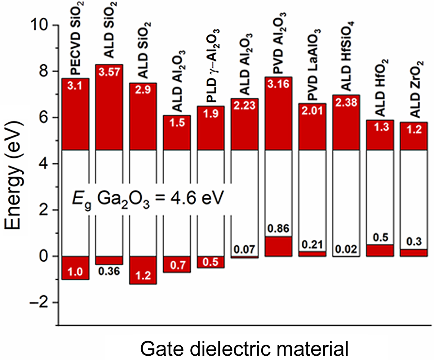
As shown in Fig. 9, there are a limited number of dielectrics with sufficient bandgaps to provide adequate conduction and valence band offsets on Ga2O3. There is definitely room to explore new options with bandgaps above 7 eV and with dielectric constants above 25. There are few choices with sufficiently high bandgap to get the desired >1 eV conduction and valence band offsets. Materials with a high dielectric constant (high-K) are desirable in Ga2O3 FETs, since the higher capacitance can reduce the effect of interface traps and therefore reduce the device operating voltage. Currently, the two most common dielectrics used are SiO2 and Al2O3. It has been found that the deposition method can have a very significant effect on the band alignment.[Reference Fares, Ren, Lambers, Hays, Gila and Pearton55–Reference Fares, Ren, Lambers, Hayes, Gila and Pearton60] There are often variations in reported valence band offsets for dielectrics on semiconductors and some of the reasons documented include metal or carbon contamination, interfacial disorder, variations in dielectric composition, thermal conditions, strain, and surface termination effects.[Reference Hays, Gila, Pearton and Ren59] Figure 10 shows there are differences of up to 1 eV in band alignments for SiO2 and Al2O3 on Ga2O3 and (Al0.14Ga0.86)2O3, depending on whether they are deposited by sputtering or Atomic Layer Deposition. In the case of Al2O3, this changed the band alignment from nested (type I) to staggered gap (type II). The valence band offset at each heterointerface was measured using x-ray Photoelectron Spectroscopy and was determined to be −0.85 eV for sputtered Al2O3 and 0.23 eV for ALD Al2O3 on β-(Al0.14Ga0.86)2O3, while for SiO2 it was 0.6 eV for sputtered and 1.6 eV for ALD. These results are consistent with recent results showing that the surface of Ga2O3 and related alloys are susceptible to severe changes during exposure to energetic ion environments.
Dielectric constants and bandgaps for different dielectrics and potential contact materials on Ga2O3.

Band alignments for common dielectrics on Ga2O3.

More work needs to be done to understand the band offsets of p-type oxide heterojunctions (CuI, Ir2O3, SnO2) on Ga2O3. From Anderson's rule,[Reference Anderson53] the conduction-band and the valence-band offsets are assumed to equal the differences of the electron affinities and the ionization energies, respectively, of the semiconductors forming the heterostructure and basically is the analog of the Schottky–Mott rule for metal–semiconductor or Schottky contacts. Monch[Reference Mönch52] has proposed an alternative approach, in which the band-structure alignment at oxide heterostructures can be explained by interface-induced gap states directly related to the electronegativities of the semiconductors involved.
Field plates, impact ionization coefficients, and role of defects
To date, only a limited number of dielectrics have been used a gate overlap field plates and the optimization of material and geometry is largely unexplored.[Reference Ghosh and Singisetti61–Reference Cao, Wang, Harden, Ye, Stillwell, Hoffman and Fay65] To understand the breakdown characteristics of a power device, it is also important to know the impact ionization coefficients of electrons and holes as a function of the electric field in the semiconductor.[Reference Ghosh and Singisetti61] There are, as yet, no experimental measurements of these quantities for Ga2O3. The phenomenon of reverse breakdown is explained by avalanche multiplication, which involves impact ionization between host atoms and high-energy carriers. When a high-energy hole or electron under high electric field impacts an electron in the valence band, it will produce a new electron–hole pair (EHP). This newly generated EHP will cause other collisions and rapidly multiply carriers. Avalanche breakdown is defined to occur when.[Reference McKay and McAfee66–Reference Chynoweth and Pearson70]
 $$\int_0^{W_D} {\alpha _p\exp \left[ {\int\limits_0^x {(\alpha_n-\alpha_p)dx}} \right]} dx \gt 1$$
 $$\alpha _i = \alpha _0\exp \left( {\displaystyle{{-b_0} \over E}} \right)$$
where W D is the depletion width, α a and α p are the ionization rates of electrons and holes. The electron ionization rate has been calculated for Ga2O3 from a Boltzmann Transport Equation approach as α n = 0.79 × 10⁶ exp ( − 2.92 × 10⁷)/E (cm−1).[Reference Ghosh and Singisetti61] Using Chynoweth's equation (α = a e −b/E),[Reference Chynoweth and McKay68–Reference Chynoweth and Pearson70] measurements for Ga2O3 epitaxial layers grown on bulk Ga2O3 substrates should produce values for α and b for the impact ionization coefficient of electrons in Ga2O3 at room temperature. Defects such as threading dislocations in the drift region of rectifiers lead to premature breakdown[Reference Grundmann, Klüpfel, Karsthof, Schlupp, Schein, Splith, Yang, Bitter and von Wenckstern71–Reference Lany78] and it will be important to measure the changes in effective impact ionization coefficients in material with known defect densities.
In the case of punch-through junction diode, the breakdown voltage is given by
 $$BV_{PT} = E_cW_{PT}-\displaystyle{{qN_BW_{PT}^2} \over {2\varepsilon \varepsilon _0}}$$
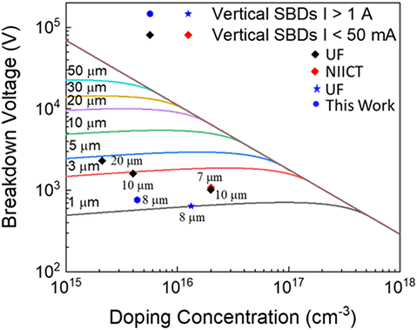
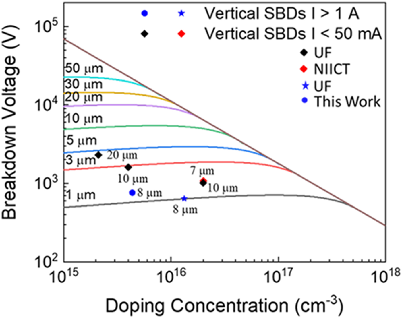
While the relevant relations are still being refined for Ga2O3, initial calculations of the same type can produce a plot of the theoretical breakdown voltage of Ga2O3 punch-through diodes as a function of doping concentration and drift region thickness. Figure 11 is a plot of the theoretical breakdown voltage of Ga2O3 punchthrough diodes as a function of doping concentration and drift region thickness, along with experimental values generated by us and others. A 3 µm epi layer with doping concentration of 1016/cm3 theoretically has ~1800 V breakdown voltage. The actual experimental value of breakdown voltage is far from these theoretical predictions and continued improvements in both materials and processing are needed to reduce this gap.[Reference Yang, Ahn, Ren, Pearton, Jang, Kim and Kuramata62–Reference Yang, Ahn, Ren, Pearton and Kuramata64]
Breakdown voltage versus drift layer thickness for vertical Ga2O3 rectifiers, with experimentally reported values.
Trench etching (plasma), digital wet etch for damage cleanup
The dry etching studies to date on Ga2O3 indicate that the etching mechanism is ion-driven, so there will be residual damage due to the ion bombardment. Optimization of the plasma conditions can minimize the amount of damage, but post-processing annealing or wet etch clean-up must be employed. In addition, β-Ga2O3 wafers are usually chemically mechanically polished and care must be taken to avoid residual damage layers. For subsequent growth or processing on these surfaces, etching and annealing to remove the damaged layer and create a step structure on the wafer surface are needed. Ohira and Arai[Reference Ohira and Arai79] examined different etching reagents and temperatures for β-Ga2O3. Only 47% HF at RT and 60.5% HNO3 at 120 °C were found produce etching. β-Ga2O3 is resistant to other acid and basic solutions at room temperature. With the use of HF, the dissolution of Ga from Ga2O3 linearly increased with etching time and with HF concentration. The etching rate of the (100) plane was found to be almost twice higher as compared to the (001) plane.
Photoelectrochemical etching has yet to be explored for Ga2O3. The dissolution rate of semiconductors may be altered in acid or base solutions by illumination with above bandgap light. The mechanism for photo-enhanced etching involves the creation of e–h pairs, the subsequent oxidative dissociation of the semiconductor into its component elements (a reaction that consumes the photo-generated holes) and the reduction of the oxidizing agent in the solution by reaction with the photo-generated electrons. Generally, n-type material is readily etched under these conditions, while p-type material is not due to the requirements for confining photo-generated holes at the semiconductor–electrolyte interface (i.e., the p-surface is depleted of holes because of the band-bending).
Plasma processing and annealing can affect background n-type conductivity
Plasma exposure generally increases the n-type conductivity of the near-surface, while annealing in O2 ambients tends to decrease this conductivity.[Reference Tadjer, Mahadik, Freitas, Glaser, Koehler, Luna, Feigelson, Hobart, Kub and Kuramata15] There are at least two sources for electrical conductivity in β-Ga2O3, namely residual impurities, such as the common hydrogenic donor impurities (ionization energy~30 meV) Si, Sn, Ge located on Ga sites, which provide the electron concentration at the level of about 1017/cm3, as well as hydrogen. The n-type conductivity can be reduced by adding the acceptors Mg, Be, and by annealing in O2.There are always native defects present prior to processing, such as the deep acceptors due to native defects V Ga, at tetrahedral (Ga1) and octahedral (Ga2) sites. Their concentration increases with the partial pressure of oxygen during growth or annealing and leads to compensation of the n-type conductivity. There are also oxygen vacancies VO at threefold coordinated sites (O1 and O2) and fourfold coordinated sites (O3). Theory indicates that all of these oxygen vacancy configurations are deep donors and have minimal effect on the conductivity. Shallow donors may include isolated Hi+, as well as V Ga-H complexes that reduce the compensation effect of Ga vacancies. Hydrogen can occupy either interstitial (Hi) or substitutional sites (HO) and in both configurations can act as shallow donors. The theory also suggests that F and Cl on the O site are shallow donors and can contribute to conductivity. Fe–doping is used to create resistive material for buffers on FETs. Hall measurements of Fe doped β-Ga2O3 indicate the material remains weakly n-type even with the Fe doping, with an acceptor energy of 860 meV relative to the conduction band for the Fe deep acceptor.
Currently, the range of carrier concentrations available in bulk β-Ga2O3 are 1016–1019/cm3, while in epitaxial layers it is from 1016 to 1020/cm3, with maximum electron mobilities of 150–170 in bulk samples and 120–130/cm2/V/sec in epitaxial layers.
Conclusions
Although high breakdown voltage devices can be fabricated using only majority carrier semiconductors,[Reference Hu, Nomoto, Li, Zhang, Tanen, Thieu, Sasaki, Kuramata, Nakamura, Jena and Xing80] low on-resistance is difficult to achieve without minority carriers. The absence of p-Ga2O3 is a major limitation. The low thermal conductivity is another major limitation. Process developments in Ohmic and rectifying contacts, gate dielectrics, and ion implantation continue to help improve device performance.
A challenge to the commercial viability of Ga2O3 is the lack of a diverse supply chain for wafers and epi films.[Reference Tadjer81] Only one company provides Ga2O3 substrates commercially, Tamura Corporation. Its spinoff, Novel Crystal Technology has commercialized Ga2O3 epilayers by molecular beam epitaxy and halide vapor phase epitaxy. The one commercial (albeit limited availability) Ga2O3 device is a rectifier fabricated using α-Ga2O3 grown by mist-CVD by Flosfia, Inc. Northrop Grumman Synoptics has demonstrated Czochralski grown 2-inch boules of β-Ga2O3, but these are not commercially available.[Reference Tadjer81] Agnitron has commercialized an MOCVD system.[Reference Tadjer81] Kyma Technologies and Structured Materials Industries have demonstrated a high-quality material. It will take a continued investment to allow maturity of Ga2O3 device technology. Ga2O3 will not displace SiC and GaN devices but possibly supplement them at high voltages.
Acknowledgments
The work at UF is partially supported by Department of the Defense, Defense Threat Reduction Agency, HDTRA1-17-1-0011 (Jacob Calkins, monitor).