
Introduction
During the last decade, organic semiconductors have gained considerable attention as an active layer for next-generation electronics due to ease in their patterning and their tunable molecular structure, flexibility, light-weight, and large-area applicability.[ Reference Voss 1 – Reference Jung, Na, Baeg, Kim, Yoon, Kim, Kim and You 4 ] In particular, their promising potential low-cost is expected to begin an era of disposable electronics.[ Reference Kim, Moon and Han 5 , Reference Forrest 6 ] Organic radio-frequency identification (RFID) tags, which can be used to detect objects automatically in the near-field region (<10 m), are one of the emerging applications in disposable electronics. For this reason, organic RFID tags have been extensively studied over the past few decades.[ Reference Myny, Rockelé, Chasin, Pham, Steiger, Botnaras, Weber, Herold, Ficker, Der Van Putten, Gelinck, Genoe, Dehaene and Heremans 7 – Reference Myny, Steudel, Vicca, Beenhakkers, van Aerle, Gelinck, Genoe, Dehaene and Heremans 11 ]
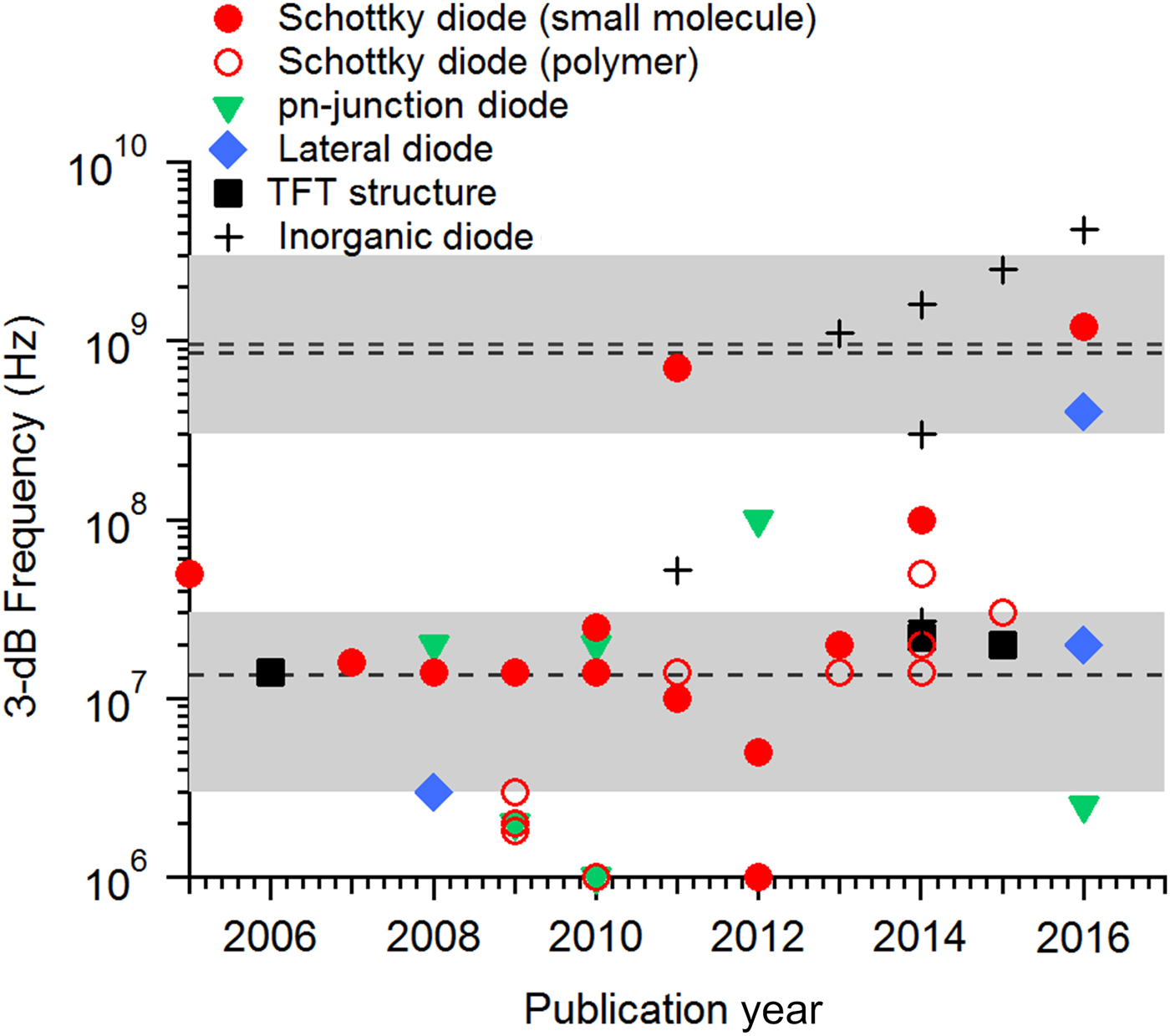
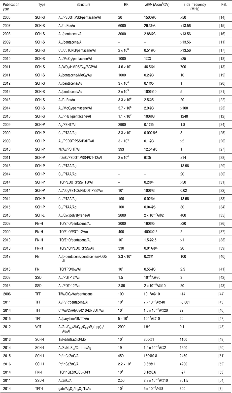
To realize organic RFID tags at the standard frequency of 13.56 MHz for high-frequency (HF) systems and 860–960 MHz for ultra-high-frequency (UHF) systems, organic rectifiers that convert radio frequency (RF) signal to DC power for operating circuits in the tags should be properly operated at the given frequency. Figure 1 and Table I summarize previously published characteristics of organic rectifiers, including the 3 dB frequency, at which the output voltage drops to half. Although different types of organic rectifiers have been proposed, the organic rectifiers with a vertical Schottky diode structure have been the most commonly reported devices because of their structural advantages in frequency characteristics. Most of the organic rectifiers have been HF systems due to the limited charge-transport properties and, hence, the operating frequencies of RFID tags have mainly been distributed around 13.56 MHz.[ Reference Fiore, Battiato, Abdinia, Jacobs, Chartier, Coppard, Klink, Cantatore, Ragonese and Palmisano 9 – Reference Myny, Steudel, Vicca, Beenhakkers, van Aerle, Gelinck, Genoe, Dehaene and Heremans 11 ] The HF RFID systems use inductive coupling for communication between a reader and a tag that can be operated only in the near field (<1 m). To achieve longer operating distances, the operating frequency should be increased to the UHF region where the RFID systems can communicate using backscattering modulation. However, conceiving UHF RFID tags still remains a challenge due to the difficulty in fabricating ultrafast organic rectifiers, whose operating frequencies scale with their charge-transport properties. These are largely affected by metal/organic and organic/organic interface properties in the organic rectifiers. By modifying the interface properties of the organic rectifiers through interface engineering, organic rectifiers operating in the UHF region can be achieved.[ Reference Kang, Wade, Yun, Lim, Cho, Roh, Lee, Nam, Bradley, Kim and Lee 12 , Reference Im, Moon, Shin, Kim and Yoo 13 ]
Frequency characteristics of organic rectifiers published over time. The gray shades indicate the range of the HF and UHF bands and the dashed lines denote the standard frequencies.
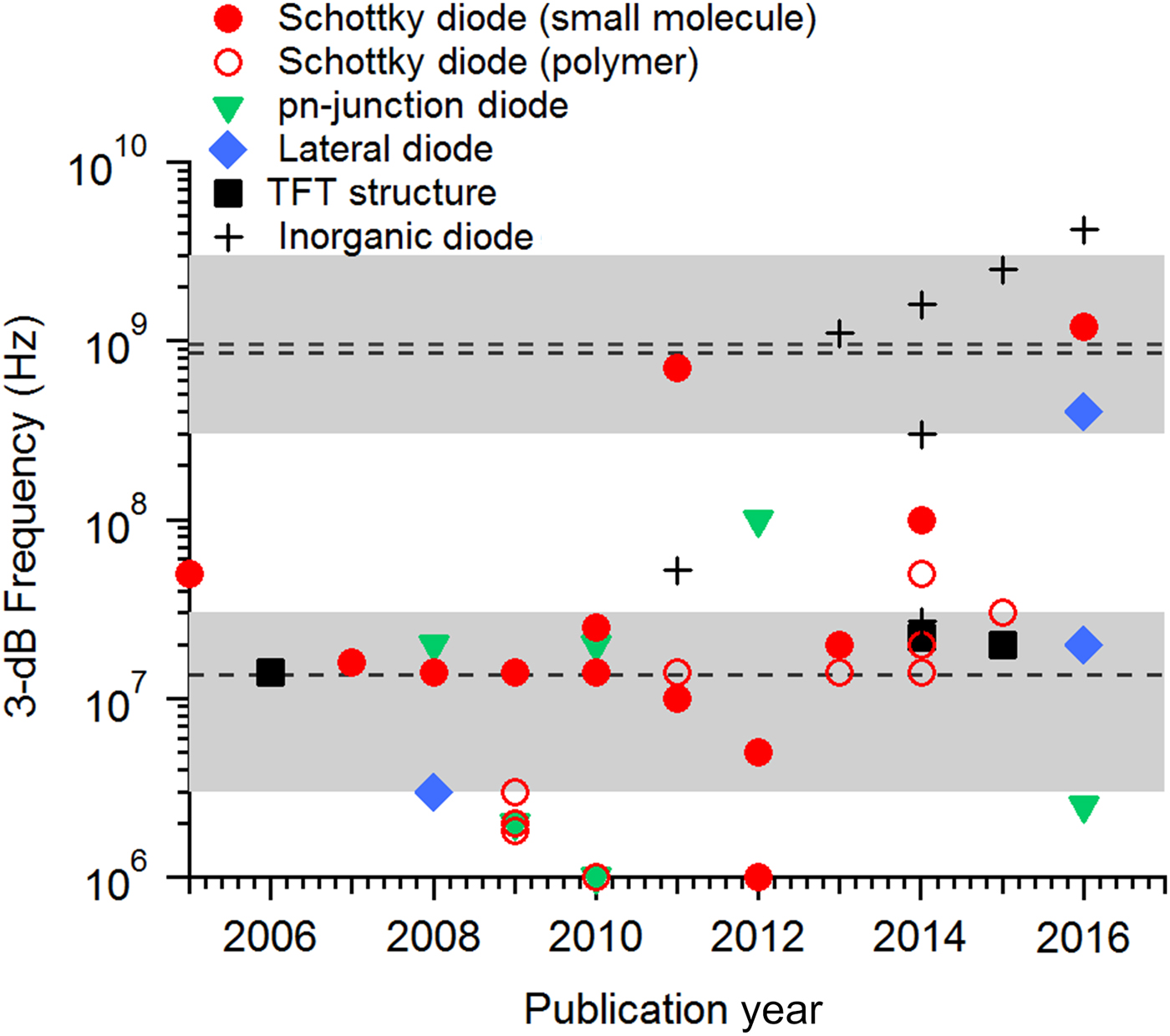
Summary of previously published characteristics of organic rectifiers. For comparison, recent progress of thin film or printable inorganic rectifier is included.

SCH-S: Schottky diodes based on small molecules; SCH-P: Schottky diodes based on polymers; SCH-L: lateral Schottky diodes; PN-H: organic/inorganic hybrid pn-junction diodes; PN: organic pn-junction diodes; SSD: organic self-switching devices; TFT: organic TFTs with diode connection; VOT: vertical organic transistors with diode connection; SCH-I: inorganic Schottky diodes; PN-I: inorganic pn-junction diodes; SSD-I: inorganic self-switching devices; TFT-I: inorganic TFTs with diode connection; BCP: 2,9-dimethyl-4,7-diphenyl-1,10-phenanthroline; TFB: poly(fluorene-alt-triarylamine); FS102: amorphous co-polymer of arylamine and a fused aromatic species (Flexink Ltd., U.K.); p-pentacene: 2,2-(perfluoronaphthalene-2,6-diylidene) dimalononitrile doped pentacene; W2(hpp)4: tetra-kis(1,3,4,6,7,8-hexahydro-2H-pyrimido[1,2-a]pyrimidinato) ditungsten(II); n-C60: W2(hpp)4 doped C60; TPD: N,N′-bis(3-methylphenyl)-N,N′-diphenylbenzidine; PVP: poly 4-vinylphenol; C10-DNBDT: 3,11-didecyldinaphtho[2,3-d:2′,3′-d′]benzo[1,2-b:4,5-b′]dithiophene; DNTT: Dinaphtho[2,3-b:2′,3′-f]thieno[3,2-b]thiophene.
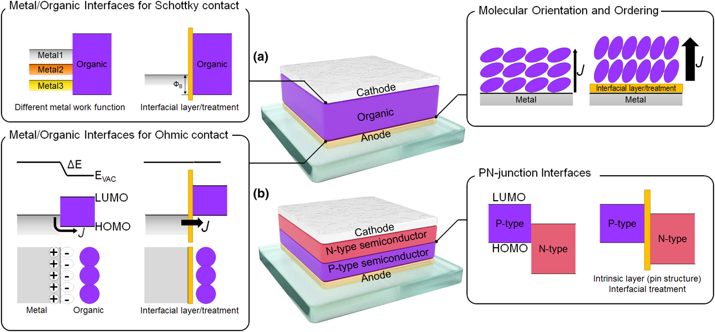
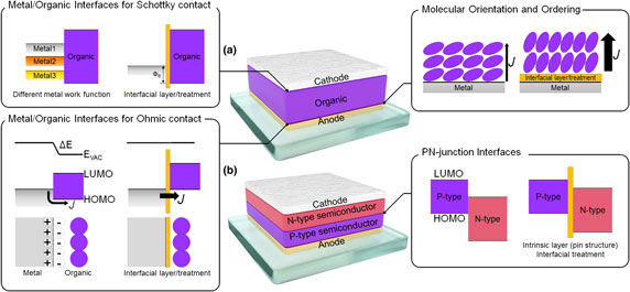
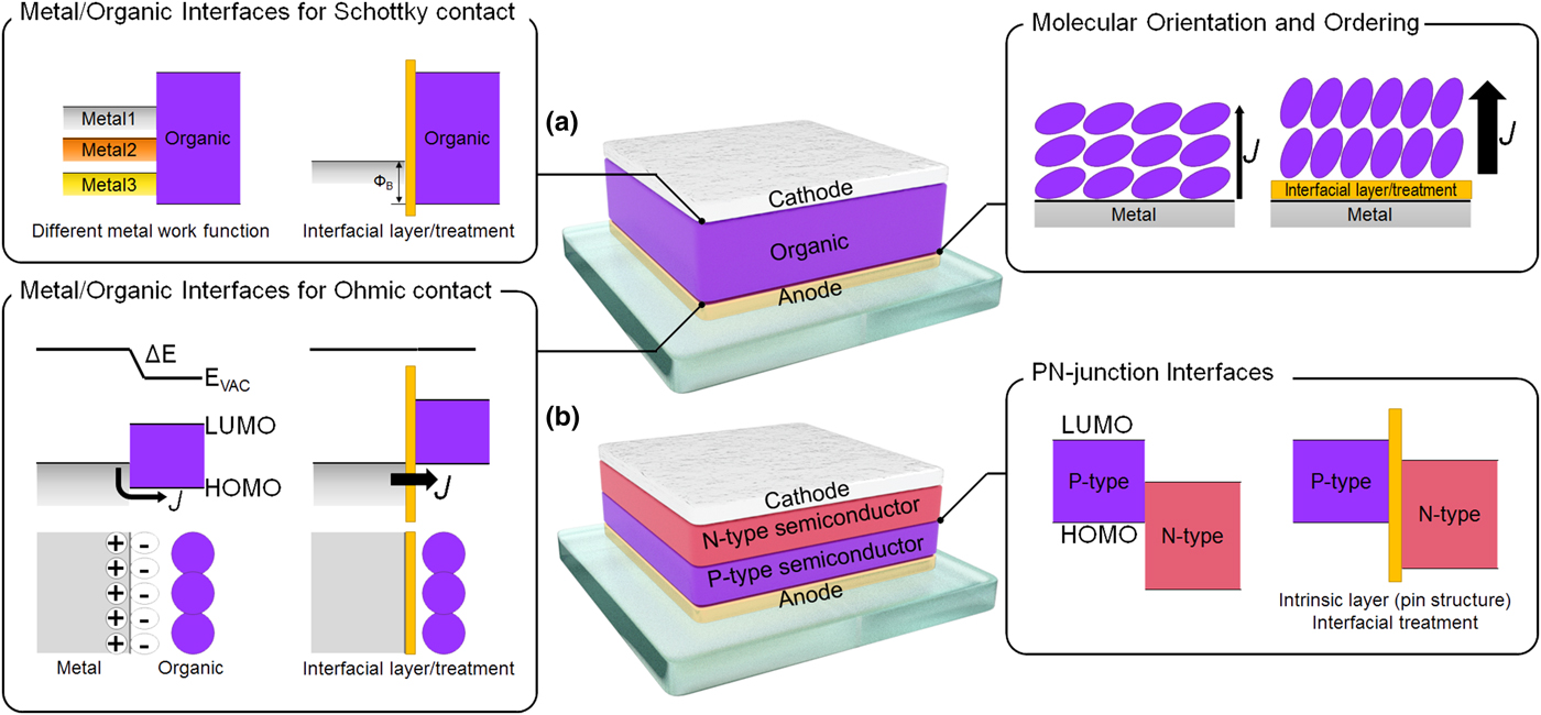
In organic devices, the interface is one of the most important factors determining their electrical properties. For example, formation of an injection barrier at metal/organic interfaces can hinder charge injection. Even if the work function of a metal electrode is matched with the highest occupied molecular orbital (HOMO) or the lowest unoccupied molecular orbital (LUMO) level of the organic semiconductor, an adversely aligned interfacial dipole can shift the vacuum level to an undesirable direction and introduce an additional energy barrier, limiting charge injection.[ Reference Diao, Frisbie, Schroepfer and Paul Ruden 55 – Reference Ishii, Sugiyama, Ito and Seki 57 ] To overcome this issue, modifying the interfacial dipole or the insertion of a carrier injection layer can be employed.[ Reference Kang, Wade, Yun, Lim, Cho, Roh, Lee, Nam, Bradley, Kim and Lee 12 , Reference Steudel, Myny, Arkhipov, Deibel, De Vusser, Genoe and Heremans 14 , Reference Kang, Hong and Lee 18 ] The current density and rectification ratio (RR) of the organic diodes can also be designed by controlling the built-in potential formed at the metal/organic or organic/organic interfaces.[ Reference Im, Moon, Shin, Kim and Yoo 13 , Reference Ma, Ouyang and Yang 58 – Reference Pandey, Mishra, Tiwari and Prakash 60 ] Moreover, the molecular orientation and alignment that determine the carrier mobility are much affected by the surface property of the underlying layer, which can be modified via interface engineering.[ Reference Kang, Wade, Yun, Lim, Cho, Roh, Lee, Nam, Bradley, Kim and Lee 12 , Reference Don Park, Lim, Lee and Cho 61 ] Because of its importance, studies on interface engineering of organic rectifiers, summarized in Fig. 2, have been intensively conducted.
Summary of interface engineering for organic rectifiers, where ΦB is the Schottky barrier height and J is the current density. (a) Structures of the Schottky diode and (b) pn-junction diode.
In this paper, we summarize the state-of-the-art of organic rectifiers, especially focusing on the interface engineering. First, background knowledge of the organic diode and structural advantages and disadvantages of organic rectifiers are discussed. Then, key factors that influence the frequency performance of the organic rectifiers are described. Next, interface engineering for HF organic rectifiers is reviewed in detail. Finally, a summary and prospects for the realization of HF organic rectifiers are presented. In this paper, we focus on interface engineering for the vertical diode structure, as a large number of interface studies on TFT structures have already been reported[ Reference Don Park, Lim, Lee and Cho 61 – Reference Liu, Xu and Noh 63 ] and the vertical diode structure is mainstream in organic rectifiers.
Basic background of organic rectifiers
Metal/organic interfaces
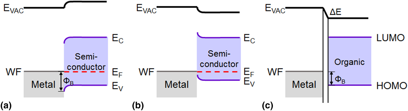
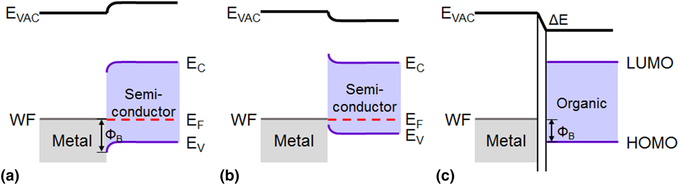
A standard model for a metal/semiconductor junction is well established in solid-state physics. When the metal/semiconductor junction is formed, the free charge carriers in the semiconductors transfer to align the Fermi level (EF) of the semiconductor with the work function (WF) of the metal, generally resulting in energy band bending. If the WF is smaller than the EF of the p-type semiconductor, electrons in the metal are transferred to the semiconductor, forming a Schottky barrier (ΦB), as shown in Fig. 3(a). This is called a Schottky contact. Whereas, if the WF is larger than the EF of the p-type semiconductor, it forms an ohmic contact, where the energy barrier can be neglected [Fig. 3(b)]. The above model is well suited for inorganic semiconductors, but in the case of organic semiconductors, this model needs to be modified, as the organic semiconductors have a large band gap (2–3 eV) and a small number of free charge carriers are thermally excited. Thus, energy band bending for the organic semiconductor is generally negligible. More importantly, the organic semiconductor interacts with adjacent materials, forming an interfacial dipole as shown in Fig. 3(c).[ Reference Ishii, Sugiyama, Ito and Seki 57 , Reference Ishii, Hayashi, Ito, Washizu, Sugi, Kimura, Niwano, Ouchi and Seki 64 ] In addition, a large number of interfacial states could result in Fermi-level pinning, such that the energy barrier at the organic/metal interface is pinned irrespective of WF. This dipole-induced energy level shift and Fermi-level pinning make the energy barrier at organic/metal interface unpredictable, and significantly affects the charge-transport properties of the organic devices. Therefore, proper modification of metal/organic interface properties is inevitable to achieve the HF organic rectifiers.
Energy level alignment at the metal/semiconductor contact for (a) the Schottky contact, (b) ohmic contact, and (c) contact with an organic semiconductor.
Charge transport in organic diodes
When the Schottky barrier is formed in the metal/organic interface and the current is limited by the injection of charges rather than the bulk of the semiconductors, the current conduction mechanism is generally governed by a thermionic emission model. This model is based on the assumption that hot carriers, which have kinetic energy larger than the barrier height, can go across the barrier and contribute to charge conduction. The current of the thermionic emission model can be expressed as Eq. (1)[ Reference Cheung and Cheung 65 , Reference Mikhelashvili, Eisenstein and Uzdin 66 ]
 $$I = I_{\rm S} \left( {\exp \displaystyle{{eV} \over {k_{\rm B} T}} - 1} \right),$$
where the I S is the saturation current, e is the elementary charge, V is the applied voltage, k B is the Boltzmann constant, and T is the temperature. I S is expressed in Eq. (2) as:[ Reference Cheung and Cheung 65 , Reference Mikhelashvili, Eisenstein and Uzdin 66 ]
 $$I_{\rm S} = AA^* T^{\rm 2} \exp \left( { - \displaystyle{{\Phi _{\rm B}} \over {k_{\rm B} T}}} \right),{\kern 1pt} \quad A^* = \displaystyle{{4\pi k_{\rm B}^2 m^*} \over {h^3}}, $$
where A is the area of the diodes, A* is the Richardson constant, ΦB is the Schottky barrier height, m* is the effective mass, and h is the Planck constant.
If the injection barrier in the metal/organic interface is small or negligible, then the metal/organic interface forms an ohmic contact and the current is limited by the bulk of the organic semiconductors rather than the metal/organic interface. At low voltages, whole charges in the bulk of the organic layer are ejected through the counterpart metal electrode; therefore, there will be no charge distribution in the organic semiconductor. In this case, the carrier transport follows Ohm's law, where the current is linearly dependent on the voltage. As the voltage increases, a greater number of charge carriers are injected before it is fully ejected, so a space charge is created. These phenomena lead to a current that is called the space-charge limited current (SCLC), which, in the case of semiconductors or insulating materials, generally follows Mott–Gurney law.[ Reference Sworakowski and Pigoń 67 ]
 $$J = \displaystyle{9 \over 8}\varepsilon _0 \varepsilon _{\rm r} \mu \displaystyle{{V^2} \over {d^3}}, $$
where ε 0 is the vacuum permittivity, ε r is the relative permittivity, μ is the carrier mobility of the organic semiconductor, and d is the thickness of the organic semiconductor. However, the actual current mechanism of the organic semiconductor is more complex because of the presence of trap states. Assuming that the traps are exponentially distributed, the current can be expressed as follows:[ Reference Sworakowski and Pigoń 67 ]
 $$\eqalign{& J \approx e^{1 - m} \mu N_{\rm C} \left( {\displaystyle{{2m + 1} \over {m + 1}}} \right)^{m + 1} \left( {\displaystyle{m \over {m + 1}}\displaystyle{{\varepsilon _{\rm 0} \varepsilon _{\rm r}} \over {N_{\rm t}}}} \right)^m \displaystyle{{V^{m + 1}} \over {d^{2m + 1}}}, \cr & m = \displaystyle{{T_{\rm t}} \over T},} $$
where N C is the effective density of conduction band states, N t is the trap density, and T t is the temperature parameter characterizing the trap distribution. When an electric field is applied, furthermore, and all of the trapping sites are filled in the organic semiconductor, the SCLC becomes independent of traps, and the equation can be simply expressed as Eq. (3).
The SCLC can be applicable when the current is dominated by drift. For organic diodes, the work function difference between the anode and cathode creates built-in potential. When the applied voltage is much higher than the built-in voltage, the current obeys the Mott–Gurney law. However, when the applied voltage is smaller than the built-in voltage, the internal electric field in the organic is negative, leading to a negative drift current. Different barrier heights at the anode and cathode contacts yield a distribution of hole density (electron density, in the case of an n-type organic material), allowing a positive diffusion current to flow. At the low-voltage region, the positive net current indicates that the dominant current mechanism is diffusion, which can be expressed as follows:[ Reference de Bruyn, van Rest, Wetzelaer, de Leeuw and Blom 68 ]
 $$\eqalign{& J = \displaystyle{{e\mu N_{\rm C} (\Phi _{\rm B} - b - V)[\exp (eV/k_{\rm B} T) - 1]} \over {d\exp (eb/k_{\rm B} T)[\exp \{ e(\Phi _{\rm B} - b)/k_{\rm B} T\} - exp(eV/k_B T)]}}, \cr & b = \displaystyle{{k_{\rm B} T} \over e}\left[ {\ln \left( {\displaystyle{{e^2 N_{\rm C} d^2} \over {2k_{\rm B} T\varepsilon _0 \varepsilon _{\rm r}}}} \right) - 2} \right],} $$
where b is the band-bending parameter. For organic diodes, therefore, the current exponentially increases in the low-voltage region [Eq. (5)] and quadratically increases in the high-voltage region [Eq. (3)] with regard to the applied voltage.
Structure of organic rectifiers
A rectifier consists of a capacitor and a rectifying diode. When a forward bias is applied to the rectifier, charges flow through the rectifier and are stored at the capacitor, but the stored charges do not discharge by the reverse bias because the diode conducts only when it is forward-biased. Several device structures and electrical circuits have been proposed to give the devices the properties of a rectifier and to improve their electrical properties.
A Schottky diode [Fig. 2(a)] is a metal/semiconductor/metal structure with a Schottky contact at the metal/semiconductor interface and is the most commonly used structure in organic rectifiers.[ Reference Myny, Steudel, Vicca, Beenhakkers, van Aerle, Gelinck, Genoe, Dehaene and Heremans 11 – Reference Li, Heljo and Lupo 30 , Reference Heljo, Lilja, Majumdar and Lupo 33 , Reference Heljo, Schmidt, Klengel, Majumdar and Lupo 34 ] The built-in potential at the Schottky contact is effectively reduced by a forward bias, which allows high current to flow that is limited by the Schottky barrier when the reverse bias is applied. The metal/organic contact at the counter electrode should be ohmic to achieve a high forward current. A Schottky diode in a vertically sandwiched structure is relatively easy to fabricate and it is facile to control the thickness of the organic layer and the device area. For these reasons, it has been the main rectifier structure adopted by many researchers. A laterally co-planar structure is tolerant of the pinholes and defects of the organic layer, which can cause high leakage current and breakdown in a vertically sandwiched structure. However, difficulty in achieving a uniform sub-micrometer gap of two different electrodes is a disadvantage of the laterally co-planar structure of the Schottky diode. Semple et al. reported a 20 nm gap co-planar diode based on solution-processed C60:polystyrene by using adhesion-lithography.[ Reference Semple, Rossbauer, Burgess, Zhao, Jagadamma, Amassian, McLachlan and Anthopoulos 35 ] Because of this short gap, an estimated 3 dB frequency of 400 MHz was accomplished.
The Schottky diode is advantageous in terms of achieving high operating frequencies due to its relatively small capacitance.[ Reference Kang, Wade, Yun, Lim, Cho, Roh, Lee, Nam, Bradley, Kim and Lee 12 – Reference Steudel, Myny, Arkhipov, Deibel, De Vusser, Genoe and Heremans 14 ] However, the relatively high leakage current of the Schottky diode can be an issue, especially at high temperature. Because the leakage current of the Schottky diode is primarily limited by thermionic injection, it could be exponentially increased as the temperature is increased.
A pn-junction diode consists of n- and p-type semiconductors sandwiched between two metal electrodes [Fig. 2(b)]. A pn-junction at the interface of the p- and n-type semiconductors generates the built-in potential, which can be decreased by a forward bias and increased by a reverse bias. Because the pn-junction has the rectification property, the metal/organic contact in the anode and the cathode should be ohmic. The advantage of the pn-junction diode is that the current can be easily controlled by adjusting the doping concentration or the thickness of semiconductor layer or by inserting an intrinsic layer.[ Reference Kleemann, Schumann, Jörges, Ellinger, Leo and Lüssem 40 , Reference Kleemann, Gutierrez, Avdoshenko, Cuniberti, Leo and Lüssem 69 ] Also, high doping concentration at the metal/organic interface guarantees a quasi-ohmic contact, enabling free choice of metal electrodes. Moreover, the pn-junction diode exhibits a small leakage current compared with the Schottky diode. The major disadvantage of the pn-junction diode is its relatively low-frequency performance due to the presence of the pn-junction capacitance. The lack of high mobility n-type organic materials is another obstacle to further improvements. Thus, p-organic/n-inorganic hybrid diodes have also been studied.[ Reference Pal, Sun, Jung, Choi, Andreou and Katz 36 – Reference Liem, Choy and Yung 39 ]
Key factors of organic rectifiers to achieve high-frequency performance
The frequency performance of organic rectifiers scale with the charge transport properties of the organic diodes and there are key factors determining these properties. To increase the forward current of an organic diode, high injection efficiency and mobility are required. In addition, the rectifying barrier height affects the forward current as well as the reverse current. The thickness of the semiconductor layer is directly related to the transit time of the device, which determines the frequency response of the rectifier. The device area is not directly related to the frequency response, but it is also an important factor. These factors will be discussed in more detail below.
Barrier height and mobility
To reduce the injection barrier height for achieving high injection efficiency, several methods have been studied such as energy level alignment using high work function metals or alloys,[ Reference Chan, Lai, Fung, Tong, Lee and Lee 70 ] thermal and electrical annealing, reducing the interface dipole via a self-assembled monolayer (SAM),[ Reference Kang, Wade, Yun, Lim, Cho, Roh, Lee, Nam, Bradley, Kim and Lee 12 , Reference Campbell, Rubin, Zawodzinski, Kress, Martin, Smith, Barashkov and Ferraris 71 – Reference Kwon, Seol, Lee and Chung 73 ] and inserting a charge injection layer such as a conducting polymer,[ Reference Steudel, Myny, Arkhipov, Deibel, De Vusser, Genoe and Heremans 14 , Reference Lin, Tsai, Lin, Chang, Yeh, Pei, Peng and Wu 28 , Reference Koch, Elschner, Schwartz and Kahn 74 , Reference Heywang and Jonas 75 ] a doped organic layer,[ Reference Kido and Matsumoto 76 , Reference Zhou, Pfeiffer, Blochwitz, Werner, Nollau, Fritz and Leo 77 ] an organic material having an intermediate energy level,[ Reference Chen and Wang 78 ] or a transition metal oxide.[ Reference Tokito, Noda and Taga 79 ] The mobility is principally determined by the intrinsic molecular structure, but it is also much affected by molecular orientation and alignment. To enhance molecular orientation and alignment, controlling the surface energy through interface engineering has been studied.[ Reference Kang, Wade, Yun, Lim, Cho, Roh, Lee, Nam, Bradley, Kim and Lee 12 , Reference Matsuhisa, Sakamoto, Yokota, Zalar, Reuveny, Lee and Someya 80 , Reference Mezour, Voznyy, Sargent, Lennox and Perepichka 81 ] The rectifying barrier height is also one of the important factors determining diode characteristics. If the forward current is limited by bulk characteristics due to low mobility, the reverse current can effectively be suppressed by increasing the barrier height.[ Reference Lilja, Majumdar, Pettersson, Österbacka and Joutsenoja 59 ] If the forward current is limited by the contact, it can be enhanced by lowering the barrier height.[ Reference Im, Moon, Shin, Kim and Yoo 13 ] The aforementioned factors can be controlled by interface engineering, which will be elaborated later.
Semiconductor layer thickness
Generally, organic semiconductors operate in the SCLC regime and obey the Mott–Gurney law given by Eq. (3). If the current of the organic diode follows the Mott–Gurney law and ignoring the leakage current, the frequency performance of the organic rectifier can be expressed by[ Reference Steudel, Myny, Arkhipov, Deibel, De Vusser, Genoe and Heremans 14 ]
 $$\eqalign{\,f_{\rm MAX} & = \displaystyle{9\mu \over 16\pi d^2 V_{\rm o}} \left[ ( - 3V_{\rm o} + V_{\rm F} ) \sqrt{V_{\rm IN}^2 - (V_{\rm o} + V_{\rm F})^2} \right. \cr &\left. \quad \hskip 3pt +\, (V_{\rm IN}^2 + 2V_{\rm o}^2) {\rm arccos} \left(\displaystyle{V_{\rm o} + V_{\rm F} \over V_{\rm IN}} \right) \right],}$$
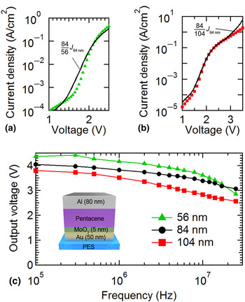
where f MAX is the maximum frequency, V O is the output voltage, V F is the transition voltage where the conduction mechanism changes from ohmic to SCLC, and V IN is the peak input voltage applied to the rectifier. From Eq. (6), the frequency response is inversely proportional to the square of the thickness. Thus, if the organic diode follows the SCLC mechanism, a thin organic layer is beneficial for the frequency performance, which is also consistent with a transit time-based equation.[ Reference Altazin, Clerc, Gwoziecki, Verilhac, Boudinet, Pananakakis, Ghibaudo, Chartier and Coppard 31 ] A large number of studies have been conducted to elucidate the effect of the thickness of the rectifiers.[ Reference Kang, Hong and Lee 18 , Reference Lilja, Bäcklund, Lupo, Hassinen and Joutsenoja 25 – Reference Kang Dae, Jae Bon, Yong-Young, Jong Keun, Yong Suk and In-Kyu 27 , Reference Altazin, Clerc, Gwoziecki, Verilhac, Boudinet, Pananakakis, Ghibaudo, Chartier and Coppard 31 , Reference Heljo, Schmidt, Klengel, Majumdar and Lupo 34 ] For solution processed organic rectifiers, where the current dominantly obeys Eq. (3) due to the low mobility (<0.01 cm2/V/s), the frequency performance increases as the thickness increases.[ Reference Lilja, Bäcklund, Lupo, Hassinen and Joutsenoja 25 – Reference Kang Dae, Jae Bon, Yong-Young, Jong Keun, Yong Suk and In-Kyu 27 , Reference Altazin, Clerc, Gwoziecki, Verilhac, Boudinet, Pananakakis, Ghibaudo, Chartier and Coppard 31 , Reference Heljo, Schmidt, Klengel, Majumdar and Lupo 34 ] For some organic materials whose current is no longer dominantly restricted by a space-charge limited mechanism, the relationship between the frequency performance and the thickness may be different. From the relationship between Eqs. (3) and (6), it can be speculated that f MAX increases as d decreases when the exponent of d in Eq. (3) is larger than 1.[ Reference Kang, Hong and Lee 18 ] In other words, the frequency performance is better when the value of the product J × d is higher. Figures 4(a) and 4(b) show measured current densities of pentacene diodes with thicknesses of 56 and 104 nm, respectively. The solid lines indicate linearly scaled current densities using J(V) = 84/56 × J 84 nm(V) or J(V) = 84/104 × J 84 nm(V), respectively, where J 84 nm(V) is the current density as a function of voltage for a diode thickness of 84 nm. Both measured current densities are under the solid lines, implying that the frequency performances are worse than that with a thickness of 84 nm, which is confirmed by the measured frequency performance as shown in Fig. 4(c). Meanwhile, a thin organic layer shows high leakage current and even breakdown due to high roughness, pinholes, and defects, thereby causing problems related to uniformity, yield, stability, and reproducibility.[ Reference Kang, Hong and Lee 18 , Reference Heljo, Schmidt, Klengel, Majumdar and Lupo 34 ] In addition, the thin organic layer decreases the reverse breakdown voltage. For example, the reverse breakdown voltages of pentacene diodes with thicknesses of 28, 56, 84, and 104 nm were reported to be 5, 14.2, 21.3, and 24 V, respectively.[ Reference Kang, Hong and Lee 18 ] Ideally, the maximum reverse bias applied to the organic rectifier is twice the peak input voltage. Thus, the reverse breakdown voltage of the organic diode should be high enough to ensure the maximum strength of an input signal at a given frequency. In summary, the frequency performance of the organic rectifier is better when the J × d value is higher, while the stability of the organic rectifier is better when the organic layer is thick. Therefore, the thickness of the organic layer should be carefully designed considering performance requirements.
(a, b) J–V curves for pentacene diodes with thicknesses of 56 and 104 nm, respectively. The solid line indicates the linearly scaled current density of the 84 nm-thick pentacene diode. (c) Frequency responses of pentacene rectifiers of different thicknesses. The inset depicts the structure of the pentacene diode.

Area of the organic diode
The frequency performance of an organic rectifier does not seem to be correlated with the area of the organic diode, which is absent in Eq. (6), but the effect of the area on the electrical properties should not be disregarded. A large diode area increases the conductance of the diode and power capacity, leading to the high output voltage and power transmission.[ Reference Kim, Cho, Hong and Lee 24 , Reference Li, Heljo and Lupo 30 ] However, the corresponding load capacitance should be kept much larger than the diode capacitance to minimize the output ripple voltage. Thus, an enlarged load capacitance owing to a large diode area increases the total area of RFID tags, which reduces price competitiveness. Furthermore, large-area diodes cannot sustain the high input voltage due to worst heat dissipation, especially on the plastic substrates having low thermal conductivity.[ Reference Kim, Cho, Hong and Lee 24 ] Hence, small-area diodes are more stable than the large-area diodes against high RF power. For these reasons, the diode area should be carefully chosen considering the input power and the power consumption of the circuits.
Interface engineering for high-frequency organic rectifiers
The electrical properties of organic rectifiers can be controlled via interface engineering. By controlling the interfacial barrier and the surface energy, the forward and reverse current levels and the molecular orientation can be adjusted.
Improving injection efficiency
Charge injection is one of the primary factors determining the performance of organic rectifiers and improving the efficiency of charge injection can help achieve HF organic rectifiers. Generally, the surface electronic cloud of metals is rearranged by a repulsion force of the organic electronic cloud that generates a dipole at the metal/organic interface, leading to a negative vacuum level shift.[ Reference Ishii, Sugiyama, Ito and Seki 57 ] As for p-type organic semiconductors, the injection barrier induced by this adversely aligned dipole limits charge injection, even if the work function of the metal and the HOMO level of the organic layer are well matched. In the case of n-type organic semiconductors, the dipole effect could be beneficial. However, if the low work function of the metal matches the LUMO level of the n-type organic semiconductor, it generally becomes vulnerable to oxygen and moisture.
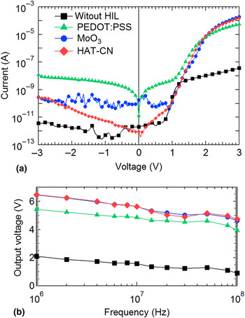
Inserting a charge injection layer is a commonly used method to improve charge injection efficiency. The dipole at an organic/organic interface is relatively smaller than the dipole at an organic/metal interface and, thus, employing an additional organic layer could be an effective way to reduce the injection barrier at metal/organic interfaces. One of the most widely used conducting polymers exhibiting a high work function and high conductivity is poly(3,4-ethylenedioxythiophene) : poly(styrenesulfonate) (PEDOT : PSS). The high carrier concentration of PEDOT : PSS allows to form a quasi-ohmic contact at the metal/organic interface and its high work function facilitates efficient hole injection from the PEDOT : PSS to the organic layer.[ Reference Steudel, Myny, Arkhipov, Deibel, De Vusser, Genoe and Heremans 14 , Reference Kang, Cho, Park, Roh and Lee 23 , Reference Lin, Tsai, Lin, Chang, Yeh, Pei, Peng and Wu 28 , Reference Kwon, Seol, Lee and Chung 73 ] In the same manner, a doped organic layer can also be used as the hole and electron injection layer.[ Reference Kleemann, Schumann, Jörges, Ellinger, Leo and Lüssem 40 , Reference Kleemann, Gutierrez, Avdoshenko, Cuniberti, Leo and Lüssem 69 ] These conductive organic layers effectively improve charge injection, but they could give rise to a lateral leakage current, resulting in a low RR.[ Reference Lin, Tsai, Lin, Chang, Yeh, Pei, Peng and Wu 28 ] Another choice for the inter-layer is a so-called charge extraction layer that exhibits deep-lying HOMO and LUMO levels and can be created using materials such as copper hexadecafluorophthalocyanine (F16CuPc), 1,4,5,8,9,11-hexaazatriphenylenehex acarbonitrile (HAT-CN), 2,3,5,6-tetrafluoro-7,7,8,8-tetracyanoquinodimethane (F4-TCNQ), or transition metal oxides. Because charge extraction layers generally have a relatively large electron affinity value, the LUMO of the charge extraction layer is matched with the HOMO of the organic layer. Thus, holes are injected by transferring electrons from the organic layer to the charge extraction layer.[ Reference Kröger, Hamwi, Meyer, Riedl, Kowalsky and Kahn 82 ] By employing the charge extraction layer, the current density of the pentacene diode was measured to be 2.9 A/cm2 at 3 V, which is orders of magnitude higher than that of the diode without the charge extraction layer (0.00057 A/cm2) [Fig. 5(a)]. As a result, the 3 dB frequency reached values of more than 100 MHz for the organic rectifier with the charge extraction layer [Fig. 5(b)].
(a) J–V and (b) frequency characteristics of the organic rectifiers with various hole injection layers (HILs).

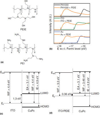
Another way to reduce the unfavorable dipole and improve hole injection is the surface treatment on the electrode. Ultraviolet ozone or plasma treatments increase OH– or O2– groups at the surface of the electrode and lead to an increment of the effective work function.[ Reference Yu, Feng, Grozea, Lu, Sodhi, Hor and Aziz 83 , Reference Ueda, Abe, Murata, Gotoh and Sakai 84 ] Chemically modified electrodes such as the Copper tetracyanoquinodimethane (CuTCNQ)-modified Cu electrode increased the effective work function from 4.6 to 5.2 eV. As a result, the forward current density of the pentacene diode with the CuTCNQ-modified Cu electrode was comparable with that with an Au electrode.[ Reference Wang, Ji, Shang, Liu, Peng and Liu 17 ] The effective work function can also be tuned by the SAM treatment by means of the permanent dipole moment of chemisorbed SAM molecules. Perfluorinated thiol derivatives are commonly used to increase the effective work function of metals because the thiol groups strongly react with metals and fluorine atoms, exhibiting high electronegativity and forming a negative dipole moment. For example, a 1H,1H,2H,2H-perfluorodecanethiol-modified Ag electrode exhibits a negative dipole moment of −1.69 D, resulting in an increased effective work function of 0.85 eV and a reduction in the hole injection barrier by 0.5 eV.[ Reference Campbell, Rubin, Zawodzinski, Kress, Martin, Smith, Barashkov and Ferraris 71 , Reference Campbell, Kress, Martin, Smith, Barashkov and Ferraris 72 ] In addition, a 2,3,4,5,6-pentafluorothiopehnol (PFBT) modified Au electrode effectively reduced the injection barrier to 0.1 eV.[ Reference Jia, Lee, Kymissis, Floreano, Verdini, Cossaro and Morgante 85 ] To improve electron injection, a thin polymer (1–10 nm) surface modifier with aliphatic amine groups such as polyethylenimine ethoxylated (PEIE) and polyethylenimine (PEI) is suitable for the air-stable electron injection layer [Fig. 6(a)]. Due to the strong molecular and interface dipole of PEIE and PEI, the effective work function of the target material can be lowered by up to 1.5 eV [Fig. 6(b)].[ Reference Zhou, Fuentes-Hernandez, Shim, Meyer, Giordano, Li, Winget, Papadopoulos, Cheun, Kim, Fenoll, Dindar, Haske, Najafabadi, Khan, Sojoudi, Barlow, Graham, Bredas, Marder, Kahn and Kippelen 86 ] As a result, insertion of a 10 nm-thick PEIE layer at an indium tin oxide(ITO)/copper(II) phthalocyanine (CuPc) interface greatly reduces the electron injection barrier from 1.3 to 0.36 eV [Figs. 6(c) and 6(d)]. This concept of the work function shifting method can also be applied to form a rectifying contact for p-type organic materials.[ Reference Matsuhisa, Sakamoto, Yokota, Zalar, Reuveny, Lee and Someya 80 ]
(a) Chemical structures of PEIE and PEI. (b) Ultraviolet photoemission spectroscopy measurements of PEIE deposited on PEDOT:PSS PH1000, ITO, and Au. Energy band diagrams of (c) ITO/CuPc, and (d) ITO/PEIE/CuPc structure, where E VAC is the vacuum level positions, E F is the Fermi level, WF is the work function, EA is the electron affinity, and IE is the ionization energy. Reproduced with permission from Ref. Reference Zhou, Fuentes-Hernandez, Shim, Meyer, Giordano, Li, Winget, Papadopoulos, Cheun, Kim, Fenoll, Dindar, Haske, Najafabadi, Khan, Sojoudi, Barlow, Graham, Bredas, Marder, Kahn and Kippelen86, Copyright 2012 AAAS.

Improving molecular orientation and crystalline order
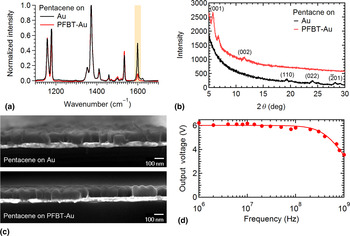
The molecular orientation and packing structure of the organic semiconductor are much affected by surface properties of the underlying layer. High packing density and long-range crystalline order are advantageous to achieve high mobility, which is favorable for the fabrication of HF organic rectifiers. Studies have shown that pentacene molecules on bare gold and SAM-modified gold exhibit different microstructures.[ Reference Kang, Wade, Yun, Lim, Cho, Roh, Lee, Nam, Bradley, Kim and Lee 12 , Reference Käfer, Ruppel and Witte 87 , Reference Hu, Tao, Hsu, Wei and Wu 88 ] For instance, Raman spectra of pentacene films on gold and PFBT-modified gold show distinctive intensity differences at 1598 cm−1 [Fig 7(a)]. Since the Raman peak at 1598 cm−1 indicates the long-axis vibration mode of pentacene, it is direct evidence of the molecular orientation change of pentacene within the PFBT-modified gold surface. In addition, the x-ray diffraction (XRD) patterns show c-axis oriented peaks of (001) and (002) planes for pentacene on PFBT-modified gold and relatively weak ab-axis oriented peaks of (110), (022), and (−201) planes for pentacene on bare gold [Fig. 7(b)]. These indicate that the pentacene molecules are likely to stand up on PFBT-modified gold and lie down on bare gold. Even if the grain sizes of pentacene on PFBT-modified gold and bare gold are the same, the charge carriers have less chance to encounter grain boundaries in a vertical direction for the pentacene film with standing up geometry, leading to an increase in mobility. The pentacene film on bare Au exhibits randomly oriented grains with the crystalline disorder. However, the pentacene film on PFBT-modified Au shows more uniform grain sizes and thicknesses [Fig. 7(c)]. Thus, the vertical mobility of the pentacene film on PFBT-modified Au is increased from 6.8 × 10⁻⁴ to 1.1 × 10⁻¹ cm2/V/s. In addition, the PFBT-modified Au electrode also effectively reduces the injection barrier as mentioned earlier, enabling diodes to reach a high-current density of 100 A/cm2 at 3 V. Owing to such a mobility improvement and the high-charge injection efficiency, a 3-dB frequency of 1.24 GHz was achieved for the pentacene rectifier with PFBT-modified Au [Fig. 7(d)]. Another interesting study reported that the performances of Au/PEIE/CuPc/Au and Au/CuPc/PEIE/Au organic diodes, which have the same structures but with different deposition order, are very different.[ Reference Matsuhisa, Sakamoto, Yokota, Zalar, Reuveny, Lee and Someya 80 ] The grazing incidence XRD patterns showed that the CuPc film on the PEIE/Au surface exhibited edge-on orientation, while the film on a pristine Au surface exhibited a higher fraction of face-on orientation, which is better for charge transport in the vertical direction. Therefore, the former structure showed a lower RR of 1.8 × 10⁴ and a forward current density of 3.0 × 10⁻³ A/cm2, but the latter structure presented a higher RR of 6.7 × 10⁷ and a forward current density of 20 A/cm2 at 2 V.
(a) Raman spectra and (b) XRD patterns of the pentacene films on PFBT-Au and Au. (c) Cross-sectional SEM images of pentacene films on PFBT-Au and Au. (d) Frequency response of the pentacene rectifier with PFBT-modified Au.

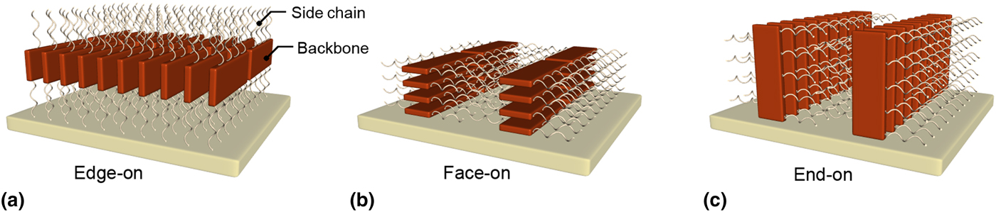
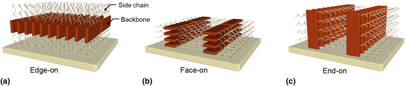
For the fabrication of low-cost organic rectifiers, conjugated polymers are one of the most important candidate materials. Recently, the mobility of the polymer semiconductor has dramatically improved to above 10 cm2/V/s.[ Reference Kim, Kang, Dutta, Han, Shin, Noh and Yang 89 , Reference Luo, Kyaw, Perez, Patel, Wang, Grimm, Bazan, Kramer and Heeger 90 ] This was accomplished on the basis of understanding of the molecular structure and orientation. Efficient intermolecular charge transfer occurs by a π–π stacking interaction. Thus, reducing the π–π stacking distance is one of the key aspects to achieving high mobility. High-mobility polymers have been reported in the TFT structures, where the edge-on orientation [Fig. 8(a)] is preferable to minimize the π–π stacking distance along the lateral direction. Insertion of a long side chain is also a common technique for polymer TFTs, in order to form highly ordered crystalline domains.[ Reference Kang, Yun, Chung, Kwon and Kim 91 , Reference Lee, Han, Yu, Shin, Yang and Oh 92 ] However, this technique is undesirable in terms of the vertical charge-transporting devices. To improve the vertical charge transport property, face-on or end-on orientations would be preferable, as shown in Figs. 8(b) and 8(c). Skrypnychuk et al. reported that the vertical conductivity of poly(3-hexylthiophene) (P3HT) could be improved by employing a graphene electrode.[ Reference Skrypnychuk, Boulanger, Yu, Hilke, Mannsfeld, Toney and Barbero 93 ] They found that P3HT on a Si substrate predominantly had an edge-on orientation, whereas that on graphene exhibited a mixed edge-on and face-on orientations. The presence of face-on aggregates can create continuous pathways in the vertical direction, leading to improved vertical conductivity from 2.2 × 10⁻⁴ to 4.1 × 10⁻⁴ S/m. Another interesting method to improve the vertical charge transport is micro- or nanopatterning. Recent work showed that the vertical mobility of a spin-coated P3HT film was greatly enhanced after being imprinted with a micropatterned poly-dimethylsiloxane (PDMS) mold.[ Reference Skrypnychuk, Wetzelaer, Gordiichuk, Mannsfeld, Herrmann, Toney and Barbero 94 ] The formation of the micropillar structures partially changes the orientation of P3HT from edge-on to end-on, enabling efficient charge transport via delocalized electronic states of the conjugated polymer chain. Therefore, the vertical mobility of the micropatterned P3HT film was impressively increased from 10−4 to 3.1–10.6 cm2/V/s. Even though the performance of the diode was not optimized in terms of charge injection efficiency and thickness, such a high vertical mobility presents a bright future for realizing gigahertz-operable polymer rectifiers.
Orientation of the conjugated polymers: (a) edge-on, (b) face-on, and (c) end-on orientation.
Modifying the rectifying barrier height
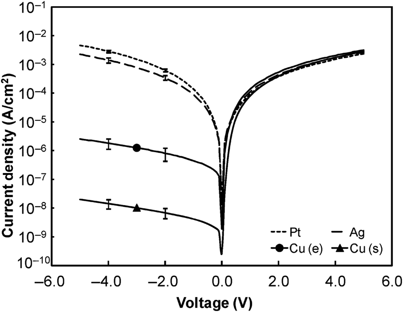
The Schottky barrier formed at the metal/organic interface imparts rectifying characteristics to the diode. The reverse current of the diode is exponentially suppressed as the Schottky barrier height increases. Thus, the Schottky barrier height should be sufficient for HF organic rectifiers. A Schottky contact can be formed by mismatching between the HOMO or LUMO levels of the organic layer and the work function of the metal. For example, the HOMO level of polytriarylamine (PTAA) is known to 5.1 eV and forms an ohmic contact with high work function metals such as platinum (5.1–6.3 eV) and printed silver (5.2 eV), which leads to no rectifying characteristics for the PTAA diode.[ Reference Lilja, Majumdar, Pettersson, Österbacka and Joutsenoja 59 ] However, a PTAA/copper electrode forms a rectifying contact, thereby reducing the reverse current significantly by 3–5 orders of magnitude (Fig. 9). Interestingly, the leakage current depends not only on the selection of the metal, but also on the metal deposition method. The sputtered copper on PTAA additionally generated a thin insulating interfacial layer, preventing charge injection from copper to PTAA, which resulted in suppression of leakage current by two orders of magnitude compared with thermally evaporated copper.[ Reference Lilja, Majumdar, Pettersson, Österbacka and Joutsenoja 59 ] The leakage current of the diode is an important issue in the rectifier because charge dissipation of the rectifier predominantly arises from the leakage current, which contributes to an additional output voltage drop.[ Reference Kang, Wade, Yun, Lim, Cho, Roh, Lee, Nam, Bradley, Kim and Lee 12 ] In fact, the output voltage of the rectifier can be dropped more than expected because Joule heating by power consumption increases the temperature of the diode—the leakage current of the Schottky diode increases exponentially as a function of temperature due to thermionic emission. It has been reported that the leakage current of the organic Schottky diode increases approximately 100-fold when the temperature is increased from 300 to 400 K.[ Reference Farag and Yahia 95 ] Thus, in terms of suppression of the leakage current, the barrier height of the organic diode should be high enough.
J–V characteristics of the PTAA diode with different cathodes. Reprinted with permission from Ref. Reference Lilja, Majumdar, Pettersson, Österbacka and Joutsenoja59, Copyright 2010 American Chemical Society.

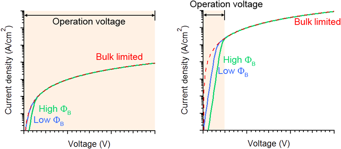
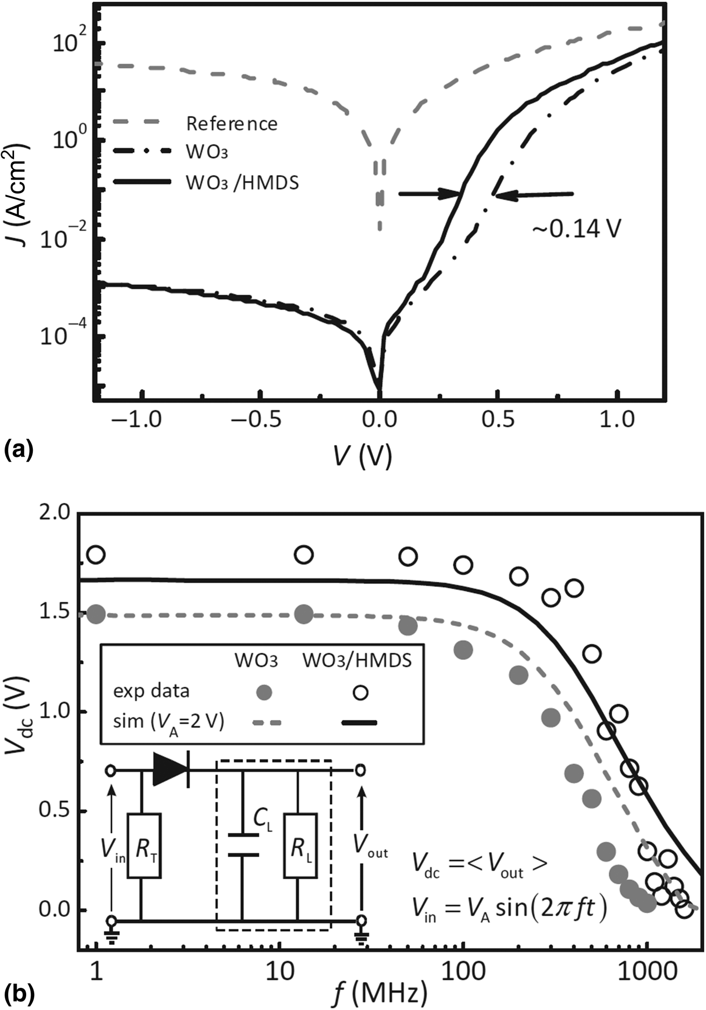
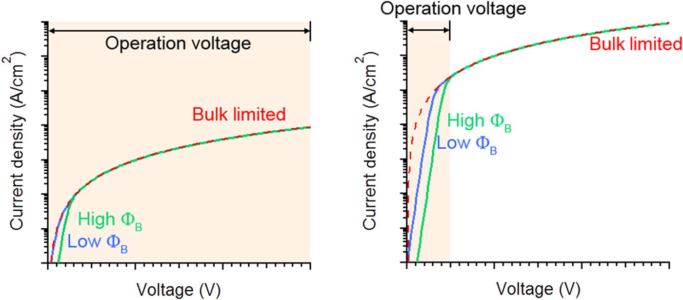
The barrier height also affects the forward current of the diode. Generally, the forward current of the organic Schottky diode is limited by either the contact or the bulk of semiconductor layer. The current is an exponential function of the voltage in the contact-limited regime [Eq. (5)] and a quadratic function of the voltage in the bulk-limited regime [Eq. (3)]. Therefore, the current predominantly obeys contact-limited in the low-voltage region and bulk-limited in the high-voltage region. If the mobility of the organic semiconductor is small, the transition voltage, where the dominant conduction mechanism changes from contact-limited to bulk-limited, is much lower so the forward current of the organic diode seems to be unchanged, even if the Schottky barrier height is changed [Figs. 9 and 10(a)].[ Reference Lilja, Majumdar, Pettersson, Österbacka and Joutsenoja 59 ] However, if this transition occurs at a voltage higher than the operating voltage of the rectifier due to high mobility, the performance of the organic rectifier is greatly affected by the barrier height. In this case, sufficient charges can be supplied to the rectifier at a low voltage; thus, the operation voltage range for a charging period is much lower than in an organic rectifier with low mobility [Fig. 10(b)]. This indicates that the current characteristics in the low-voltage region play an important role in determining the frequency performance of the organic rectifier. Figure 11(a) shows the current density–voltage (J–V) characteristics of C60 diodes with interface layers of WO3 and WO3/hexamethyldisilazane (HMDS) for rectifying contacts. Due to the dipole moment of HMDS, the effective work function of WO3/Al was shifted from 4.3 to 4.6 eV after the HMDS treatment. Compared with the forward current density of the C60 diode without the HMDS treatment, the forward current density of the C60 diode with the HMDS treatment was significantly improved below the 1-V range due to the decrease in barrier height. Moreover, the C60 rectifier with HMDS treatment showed only a 0.21 V output voltage drop and an improved 3 dB frequency of 700 MHz [Fig. 11(b)]. These results indicate that an excessively high barrier height would have detrimental effects on the performance of the high-speed organic diode. Therefore, the barrier height should be optimized to maximize the forward current, while the leakage current remains at an acceptable level.
J–V characteristics of the organic diode with (a) low mobility and (b) high mobility as a function of Schottky barrier height (ΦB). The shaded regions indicate the operation voltage region for the charging period of the organic rectifier.
(a) J–V characteristics of the diodes comprising the Al/X/C60/BCP/Al structure, where X is WO3 (dash-dot), WO3/HMDS (solid), or the absence of a layer (dash). (b) The average DC component (V dc) of the output voltage (V out) obtained for the 2 V sinusoidal incoming RF signal (V in) with regard to the operating frequency for the C60 rectifiers with and without HMDS treatment. The shapes and lines indicate the experimental and the simulation results, respectively. The inset presents the rectifier circuit diagram for measurement, which consists of the C60 diode, 500 kΩ load resistor (R L), 20 nF load capacitor (C L), and 50 Ω resistor (R T) for proper termination of the V in. Reproduced with permission from Ref. Reference Im, Moon, Shin, Kim and Yoo13, Copyright 2011 Wiley-VCH.

Organic diode with pn-junction interface
For the pn-junction diode, high mobility of p-type and n-type semiconductors is a prerequisite for a HF rectifier. Unfortunately, the development of high mobility, air-stable n-type organic semiconductors has been lagging behind compared to p-type organic semiconductors because materials having high electron affinity are generally sensitive under ambient conditions. Moreover, stacking organic materials is also an issue for the low-cost solution process because the pre-deposited organic layer can be damaged or even washed out by an organic solvent while forming the upper organic layer. To overcome these issues, various p-type organic/n-type inorganic hybrid pn-junction diodes have been proposed.[ Reference Pal, Sun, Jung, Choi, Andreou and Katz 36 – Reference Liem, Choy and Yung 39 , Reference Pandey, Mishra, Tiwari and Prakash 60 , Reference Katsia, Huby, Tallarida, Kutrzeba-Kotowska, Perego, Ferrari, Krebs, Guziewicz, Godlewski, Osinniy and Luka 96 ] Zinc oxide has widely been adopted as the n-type inorganic material for hybrid rectifiers because it possesses adequate mobility (>1 cm2/V/s) and it can be solution processed, eco-friendly, and insoluble to organic solvents.[ Reference Pal, Sun, Jung, Choi, Andreou and Katz 36 – Reference Liem, Choy and Yung 39 , Reference Pandey, Mishra, Tiwari and Prakash 60 , Reference Katsia, Huby, Tallarida, Kutrzeba-Kotowska, Perego, Ferrari, Krebs, Guziewicz, Godlewski, Osinniy and Luka 96 ] Previous reports have demonstrated pentacene/ZnO rectifiers with rectifying and switching characteristics.[ Reference Pal, Sun, Jung, Choi, Andreou and Katz 36 , Reference Lee, Park, Im, Park, Kim, Sung and Lee 38 ] A high-current density of 160 A/cm2 at 5 V and a reverse breakdown voltage of 25 V were achieved and this allowed the operating frequency to reach more than 20 MHz.[ Reference Pal, Sun, Jung, Choi, Andreou and Katz 36 ] For the solution processed p-type organic semiconductor, PEDOT:PSS, poly(3,3′-didodecylquaterthiophene) (PQT-12), and P3HT have been employed.[ Reference Sun, Pal, Jung and Katz 37 , Reference Liem, Choy and Yung 39 , Reference Pandey, Mishra, Tiwari and Prakash 60 , Reference Katsia, Huby, Tallarida, Kutrzeba-Kotowska, Perego, Ferrari, Krebs, Guziewicz, Godlewski, Osinniy and Luka 96 ] Since the charge carrier transport property of inorganic materials is superior to that of organic materials, a desirable design strategy of the hybrid diode is maximizing electron transport while the potential barrier at the organic/inorganic pn-junction properly gives the rectification behavior. Katsia et al. made a P3HT/ZnO diode with an electron barrier much lower than the hole barrier and, therefore, the electrons acted as a dominant current conduction source.[ Reference Katsia, Huby, Tallarida, Kutrzeba-Kotowska, Perego, Ferrari, Krebs, Guziewicz, Godlewski, Osinniy and Luka 96 ] A remarkable forward current density of 10,000 A/cm2 at 4 V with an RR of 105 was achieved.[ Reference Katsia, Huby, Tallarida, Kutrzeba-Kotowska, Perego, Ferrari, Krebs, Guziewicz, Godlewski, Osinniy and Luka 96 ] Improvement of electrical characteristics through energy level shifting of the pn-junction potential using the SAM treatment has also been reported.[ Reference Pandey, Mishra, Tiwari and Prakash 60 ] By employing the OTS (octadecyltrichlorosilane) treatment at the interface of ZnO/P3HT, the dipole-induced energy level shifted to lower the electron barrier, leading the hybrid pn-junction diode to achieve a 32-fold higher forward current and a 10-fold higher RR. In the case of using n-type organic materials for a pn-junction diode, C60 has been widely used, where the electron mobility can be similar to the hole mobility of p-type organic materials.[ Reference Kleemann, Schumann, Jörges, Ellinger, Leo and Lüssem 40 , Reference Kleemann, Gutierrez, Avdoshenko, Cuniberti, Leo and Lüssem 69 , Reference He, White, Wang, Zhang, Jiang and Lu 97 ] In this structure, the charge carriers are accumulated at the organic/organic interface as a consequence of the high electron and hole barriers. When the forward bias is applied, accumulated electrons and holes are non-radiatively recombined, resulting in a high forward current at low voltages. This was confirmed by fabricating hole-only and electron-only devices, where the forward current was greatly decreased compared with that for a diode, indicating that the charge injection at the organic/organic interface is almost prohibited.[ Reference He, White, Wang, Zhang, Jiang and Lu 97 ] When the reverse bias is applied, charge injection is limited by the injection barrier at the metal/organic interfaces. As a result, an N,N′-bis(naphthalen-1-yl)-N,N′-bis(phenyl)-benzidine (NPB)/C60 pn-junction diode showed a forward current density of 500 mA/cm2 at 2.6 V and an RR of 7.8 × 10⁴.[ Reference He, White, Wang, Zhang, Jiang and Lu 97 ] The device performance can be further improved by employing a p-doped/intrinsic/n-doped (PIN) diode structure.[ Reference Kleemann, Schumann, Jörges, Ellinger, Leo and Lüssem 40 ] In this case, the metal/doped organic interfaces should form quasi-ohmic contacts, facilitating charge injection from metal to organic interfaces regardless of the metal work function. The current density and transit time of the PIN diode strongly depends on the doping concentration and thickness of the intrinsic organic layer. By optimizing the doping concentration (1 wt%) and the thickness of the intrinsic layer (90 nm), the p-doped pentacene/pentacene/n-doped C60 PIN rectifier showed an output voltage of 1.4 V at 20 MHz and even a voltage of 0.5 V at 300 MHz when an input voltage of 2 V was applied.[ Reference Kleemann, Schumann, Jörges, Ellinger, Leo and Lüssem 40 ]
Conclusions
High-frequency organic rectifiers require high forward current with low leakage current, turn-on voltage, and areal capacitance, and these can be achieved through interface engineering. The energy barrier formed at the interface can be controlled by dipole-induced energy level shift using chemical treatments or inserting a charge injection layer such as a conducting polymer, a doped organic layer, or a transition metal oxide for either high injection efficiency or rectification. Additionally, the molecular orientation and crystalline order of the organic layer can also be improved by modifying the surface properties of the bottom layer. By virtue of interface engineering, the operating frequency of the organic rectifiers has recently reached values in the GHz region, which is suitable for UHF use. However, issues such as a large output voltage drop at high frequency and stability under ambient conditions have been left unsettled to date. These issues are principally attributed to the poor mobility and instability of the organic semiconductors. However, the electrical properties and stability of organic semiconductors have rapidly been improving and will continue to be developed due to their unlimited molecular design tunability. Therefore, we are optimistic that practical use of UHF organic rectifiers will be achieved in the near future.
Acknowledgments
This work was supported by the Industrial Strategic Technology Development Program (10042537 and 10077471), ICT & R&D Voucher Program (2017-0-00836) supported by Ministry of Science, ICT and Future Planning, and the National Research Foundation of Korea (2016R1A2B3009301).