Introduction
Electrochemical reaction is conventionally used for fabricating promising nanostructures to increase device performance owing to their remarkable characteristics. Electrodeposition is a well-known technique for depositing layers and nanostructures. In particular, electrodeposition with a template can achieve mass production of nanostructures with several shapes such as rods, belts, pillars, wires, and tubes.[Reference Djenizian, Hanzu, Eyraud and Santinacci1] These fabricated nanostructures have been applied to probes,[Reference Motoyama and Prinz2] biosensing,[Reference Zhang, Li, Bourgeois, Wang and Webley3] and gas sensors.[Reference Atashbar and Singamaneni4] In contrast, green fabrication of nanostructures is desirable for the conservation of energy and resources. Although electrodeposition is very efficient, the process of liquid waste disposal is time-consuming and requires enormous effort. In terms of the lean fabrication of nanostructures, electrochemical migration (ECM) has recently attracted increasing attention.
ECM is a form of corrosion accompanied by processes such as anodic dissolution, migration, and precipitation of metals and/or metallic compounds under direct current (DC) electric field and the presence of pure water.[Reference Takemoto, Latanision, Eagar and Matsunawa5,Reference Abbel, van de Peppel, Kirchner, Michels and Groen6] In the process of anodic dissolution, the metallic ions eluted from the anode electrode diffuse toward the cathode electrode via water. Migrating ions reach the cathode and metals and/or metallic compounds precipitate with reduction by the receiving electrons. The precipitated metals and/or metallic compounds grow to form nanostructures such as dendrites with a fractal pattern, progressing via water and sponges deposited on the cathode surface, which increase the surface-to-volume ratio on the cathode surface. The growth of nanostructure owing to ECM causes the insulation in electronic devices to deteriorate, resulting in short circuits by bridge formation by nanostructures; thus, ECM should be suppressed to enhance electrical reliability.
As a green method for fabricating nanostructures, ECM has been utilized to obtain hybrid Cu–Cu2O[Reference Aoki, Li and Saka7–Reference Aoki, Li and Saka9] and Ag[Reference Nakajima, Li and Saka10,Reference Nakakura and Saka11] nanostructures with several shapes such as dendrites, needles, and sponges in a pure deionized (DI) water system, without electrolyte with metallic salts. Nakakura and Saka[Reference Nakakura and Saka11] apply this method to a transparent conductive film. To generate nanostructures with desired shapes, the effects of DC voltage and temperature on the morphology of nanostructures were investigated.[Reference Aoki, Li and Saka9,Reference Nakakura and Saka11] In particular, this work discusses mechanical strain as a promising parameter contributing to the control of ECM.
Mechanochemical behavior in an electrochemical reaction has been studied for increasing the reliability of mechanical systems against environmental sensitivity in terms of stress corrosion cracking, hydrogen embrittlement, and corrosion fatigue.[Reference Despic, Raicheff and Bockris12,Reference Bockris and Subramanyan13] Plastic strain is targeted in studies because the influence of plastic strain on electrode reaction is more significant than that of elastic strain.[Reference Fryxell and Nachtrieb14–Reference Ohtani16] The anodic dissolution rate has been reported to increase linearly in the plastic region.[Reference Hoar and Scully17,Reference Raicheff, Damjanovic and Bockris18] The effect of strain on anodic dissolution has been investigated under plastic deformation to solve practical issues. To our knowledge, only a few studies have targeted the anodic dissolution after plastic deformation[Reference Gutman, Solovioff and Eliezer19,Reference Nazarov, Vivier, Thierry, Vucko and Tribollet20] ; the anodic dissolution behavior after plastic strain can be utilized for controlling the behavior of ECM.
The main aim of this work is to elucidate the effect of plastic deformation on anodic dissolution in ECM by measuring the mass of electrodes before and after the ECM tests. The deposits, which are nanostructures that precipitate on the cathode electrode, are analyzed using microscopy techniques. An empirical formulation is proposed to predict the behavior of anodic dissolution with plastic strain.
Experimental procedure
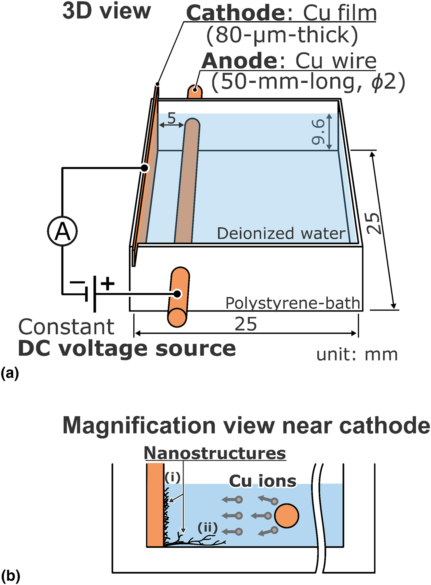
Figure 1 shows the ECM setup. The ECM was demonstrated by the rod/film[Reference Kimura and Saka21] water-drop test (WDT), which was proposed on the basis of film/film[Reference Fukaya, Aoki, Kimura and Saka8,Reference Aoki, Li and Saka9] WDT for large-scale fabrication. A Cu rod with a diameter of 2 mm and a length of 50 mm was used as the anode electrode from which Cu ions eluted with oxidation by a DC electric field. A Cu film with an area of 25 mm × 9.6 mm and a thickness of 80 µm was used as the cathode electrode, where the Cu atoms and/or Cu-based compounds precipitated by reduction formed as deposits. The anode rod was plastically deformed with tensile plastic strain ε p of 0%, 0.63%, 1.25%, 7.50%, and 10.30% and a specific angle of twist. θ p as 0, 0.37, 0.74, 1.11, and 7.39 rad/cm. The influence of plastic deformation on anodic dissolution was quantitatively evaluated via the measurement of mass change before and after the experiments using an electronic weighing instrument (A&D Company, Limited, Tokyo, Japan; Micro Analytical Balances BM-20).
Schematics of the experimental setup of the rod/film WDT: (a) 3D view of WDT setup; and (b) magnification view near cathode electrode showing nanostructures grown as (i) deposits on the electrode surface and (ii) dendrites on the bottom surface toward anode from cathode.
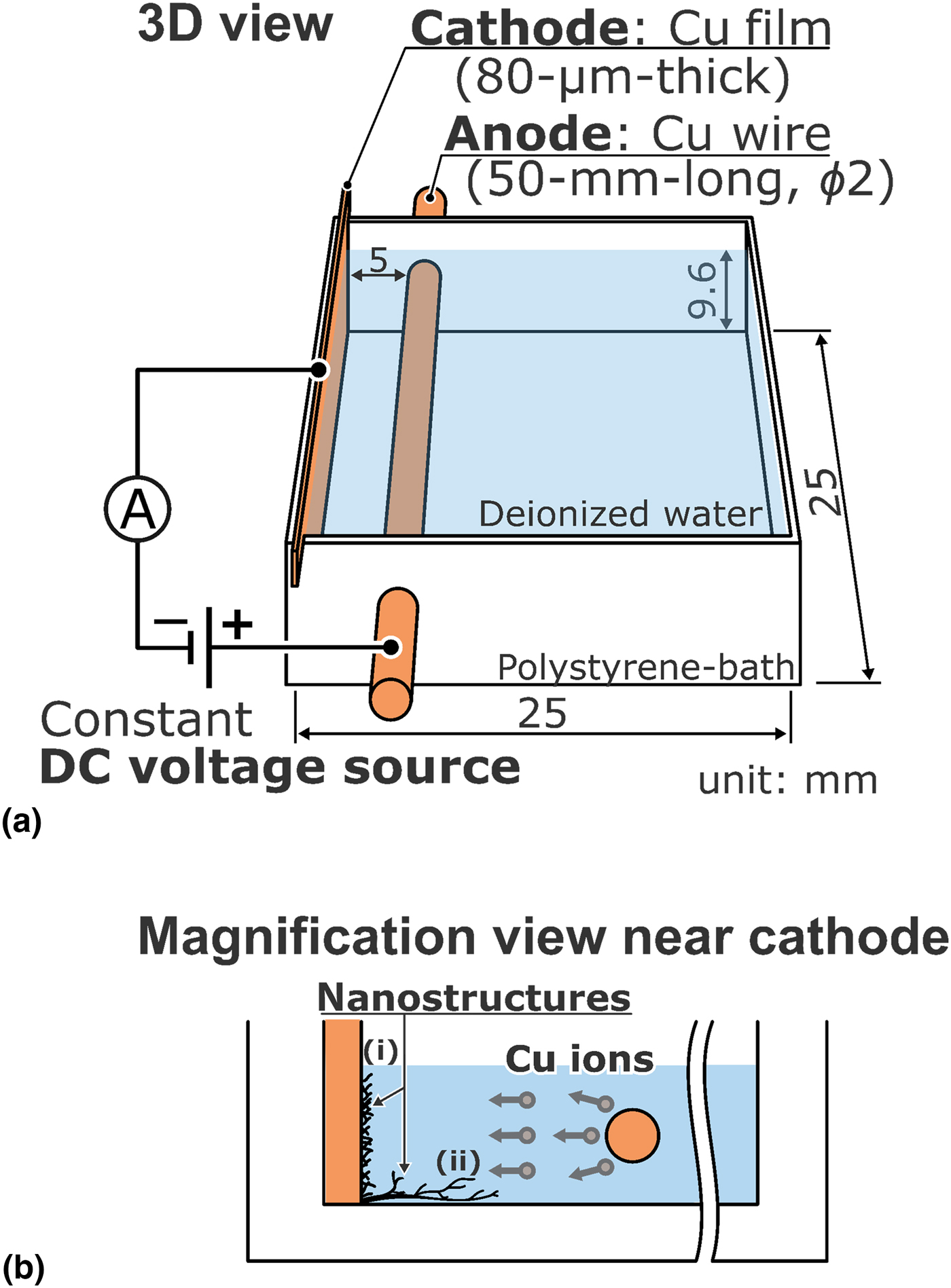
The anode rod, cathode film, and reaction cell were cleaned ultrasonically with DI water and dried in air. The anode rod and cathode film were fixed to the polystyrene reaction cell, and 6 mL of DI water with an electrical resistivity of 8 MΩ·cm was added to the cell. A DC voltage of 15 V for the ECM test was applied for 30 min by a DC power supply (Texio Technology Corporation, PAR-A series Regulated DC Power Supplies) at room temperature. The nanodeposits formed were analyzed using field-emission scanning electron microscopy (FE-SEM).
Results and discussion
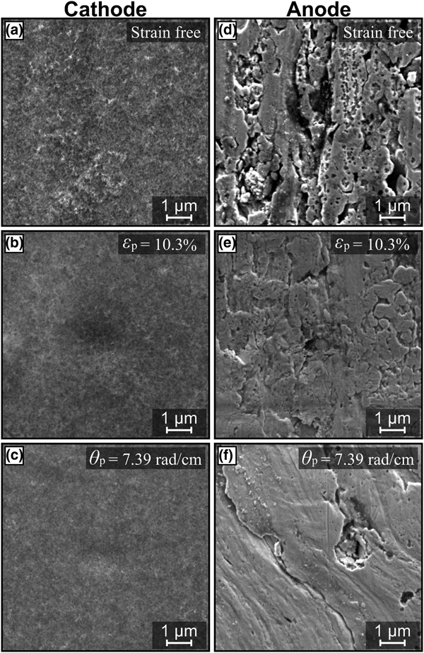
Figure 2 shows higher magnification views of the experimental results for precipitated deposits on the surfaces of cathode films and anode rods. The sponge deposits are densely precipitated on the surfaces of cathode films with an increase in ε p and θ p, as shown in Figs. 2(a)−2(c). The reacted surface with small holes where ions might be eluted is observed on the surfaces of anode rods, as shown in Figs. 2(d)−2(f).
FE-SEM images of higher magnifications on the surfaces of (a)–(c) cathode films with precipitated deposits and (d)–(f) anode rods with small holes: (a) and (d) strain free, (b) and (e) ε p = 10.3%, and (c) and (f) θ p = 7.39 rad/cm.

Aoki et al.[Reference Aoki, Li and Saka9] performed the structural analyses to detect the elements, composition, and crystalline structure via fabricating hybrid Cu–Cu2O deposits by ECM. The experimental apparatus and materials were similar to those used in the present study. X-ray diffraction and transmission electron microscopy revealed that the deposits precipitated by ECM mainly consisted of Cu with some amount of Cu2O generated by surface oxidation: the previous report[Reference Aoki, Li and Saka9] shows the different atomic percentage between the inside (Cu:O = 93.34:6.66) and the surface (Cu:O = 52.79:47.21). As previously reported by Aoki et al.,[Reference Aoki, Li and Saka9] it is presumed that the major element in precipitated deposits is Cu and the deposits are polycrystalline.
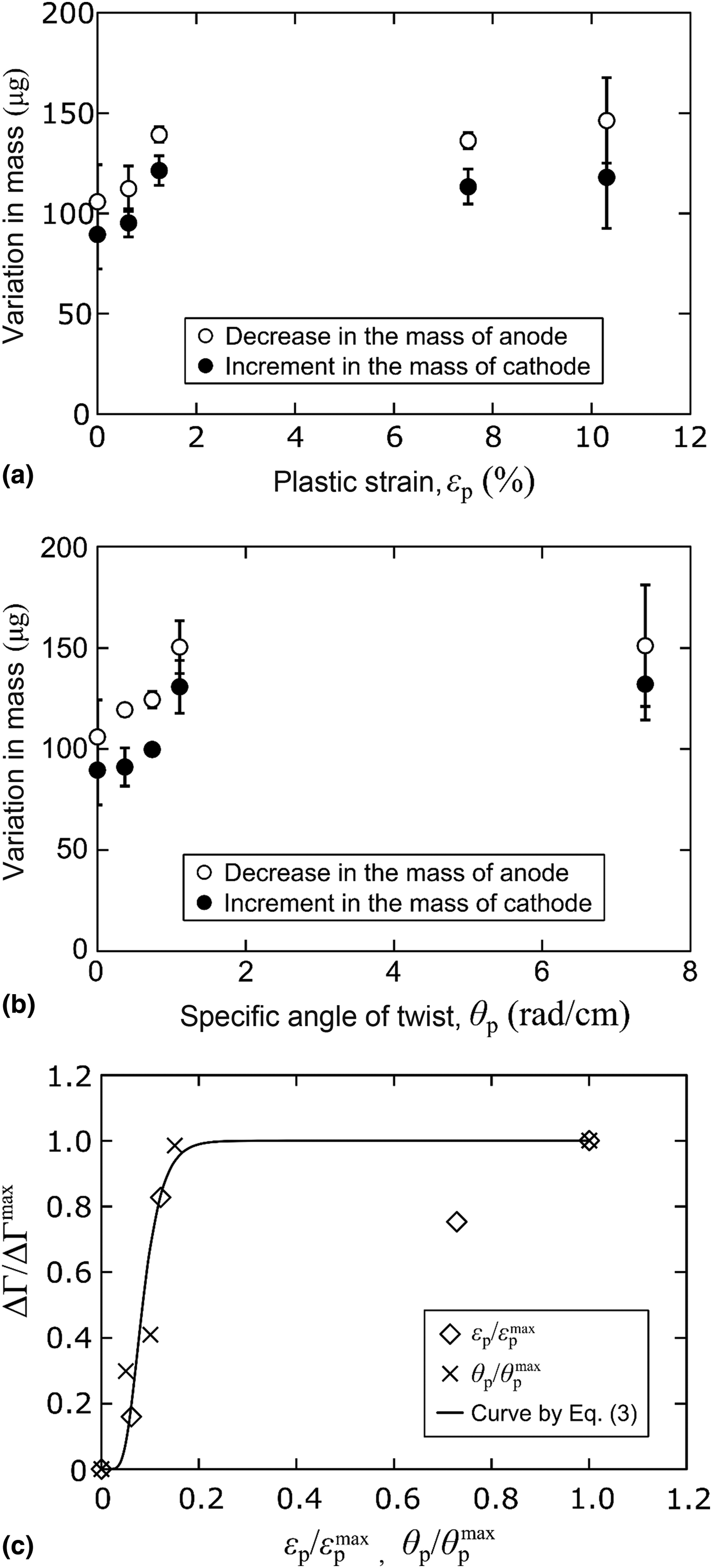
Figures 3(a) and 3(b) show an increase in the mass of the cathode and the decrease in the mass of the anode in terms of ε p and θ p. In the cases of ε p and θ p, the variations of the mass of the electrodes increase monotonically up to 1.25% and 1.11 rad/cm, respectively, but are saturated at values greater than these. The variation in the mass of the anode in Figs. 3(a) and 3(b) differs from that of the cathode because the eluted ions and dendrites that progress into the water were not measured, i.e., the amount of anode equals the amount of cathode, eluted ions, and grown dendrites. The average increments in the mass of the anode were approximately 30 and 40 µg for ε p and θ p, respectively. The increase in the error bar for mass at the maximum strain is related to the unstable behavior of anodic dissolution. Unstable fracture prior to the breaking of rods appears to affect the behavior of anodic dissolution by drastically increasing the surface area. The interesting results include the increment in the variation of mass and the saturation with plastic deformation, thus, showing the acceleration and saturation of anodic dissolution.
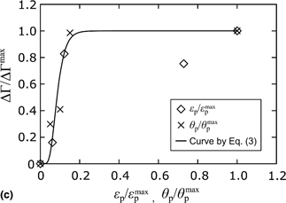
Relationships between the variation in the mass of cathode and anode electrode and (a) ε p and (b) θ p. Open and filled circles denote the decrease in the mass of anode and the increment in the mass of cathode, respectively. At least three data points were used to represent standard deviation error bars. (c) ΔΓ/ΔΓmax versus ε p/ε pmax and θ p/θ pmax relationships with experimental data of anode in Fig. 2, and the curve drawn by Eq. (3) using Q = 1.0 × 10⁻¹⁹, p = 0.8, and q = 24.

Despic et al.,[Reference Despic, Raicheff and Bockris12] Ohtani,[Reference Ohtani16] and Murata[Reference Murata22,Reference Murata23] reported that the cause of anodic dissolution under plastic strain is classified into two categories: the increase in the active point for unpassivated electrodes and the initiation of nascent surfaces for passivated electrodes. The test for investigating the effect of plastic deformation of electrodes on anodic dissolution in this work differs from that reported in previous studies[Reference Despic, Raicheff and Bockris12,Reference Ohtani16,Reference Murata22,Reference Murata23] ; while the present work focuses on the electrodes after plastic deformation, the previous studies considered the electrodes under plastic deformation. The Cu rod of the anode electrode has a natural oxide layer as passivation; therefore, the passivation fracture with plastic deformation contributes to facilitating the anodic dissolution. In the case of passivated electrodes, the acceleration of anodic dissolution with increasing ε p and θ p is speculated to be caused by the generation of new active sites on the surface, such as surface roughness, edges of slip step accompanied by dislocations, and high-index planes where ions elute easily. For Cu, the linear increase rate of anodic dissolution with plastic deformation is slower than that of Fe.[Reference Despic, Raicheff and Bockris12,Reference Bockris and Subramanyan13] This is due to the existence of high-index planes that act as high dissolvers[Reference Bockris and Subramanyan13] in Fe, but not in Cu. Thus, the high-index planes were not to be considered in this study of Cu. The surface roughness and the edges of slip step are assumed to work as highly localized dissolvers creating nascent surfaces in Cu. These non-protected regions result in rapid local dissolution. Eventually, the rapid local dissolution with plastic strain is reflected in the increase of the mass of the cathode electrode.
Conversely, the saturation of mass implies that the acceleration of the anodic dissolution due to plastic deformation is suppressed. It appears that the overlarge plastic deformation does not effectively contribute to the increase in anodic dissolution. Herein, the effect of edges of slip step together with the density of dislocations is proposed as a candidate. It is assumed that the activation energy governing dislocation motion is changed in order to saturate the anodic dissolution.
To elucidate the saturation mechanism and control the anodic dissolution by plastic deformation in ECM, a formulation was attempted. Because the thermally activated process governs the anodic dissolution[Reference Ohtani and Hayashi24] and the dislocation motion,[Reference Appel25] the anodic dissolution rate Γ(ε p) corresponding to the current density in ECM is presumed to be proportional to an exponent of ε p and thus can be expressed as follows:
 $$\Gamma (\varepsilon_{\rm p} ) = D^{\ast}\exp \left\{ {-\displaystyle{Q \over {kT}}{\left[ {1-{\left( {\displaystyle{{\varepsilon_{\rm p}} \over {\varepsilon_{\rm p}^{\ast}}}} \right)}^m} \right]}^n} \right\},$$
where D* is the diffusion coefficient including the strength of the electric field, temperature, and other influencers, Q is the activation energy, k is the Boltzmann's constant, T is the absolute temperature, ε p* is the reference value of plastic strain, and m and n are the coefficients. The difference between Γ(ε) and Γ(0), which is under free strain, is given by
 $$\Delta \Gamma = D^{\ast}\left\langle {\exp \left\{ {-\displaystyle{Q \over {kT}}{\left[ {1-{\left( {\displaystyle{{\varepsilon_{\rm p}} \over {\varepsilon_{\rm p}^{\ast}}}} \right)}^m} \right]}^n} \right\}-\exp \left( {-\displaystyle{Q \over {kT}}} \right)} \right\rangle. $$
The normalized ratio by the maximum difference, ΔΓmax [ = Γ(ε pmax)−Γ(0)], in the case where ε*p equals ε pmax, representing the maximum value of plastic strain in the experiment is given by
 $$\eqalign{\displaystyle{{\Delta \Gamma} \over {\Delta \Gamma ^{\max}}} =& \displaystyle{1 \over {1-\exp \left( {-\displaystyle{Q \over {kT}}} \right)}}\left\langle {\exp \left\{ {-\displaystyle{Q \over {kT}}{\left[ {1-{\left( {\displaystyle{{\varepsilon_{\rm p}} \over {\varepsilon_{\rm p}^{\max}}}} \right)}^m} \right]}^n} \right\} \right}\right} &\cr\quad\quad\quad\quad \left- \exp \left( {-\displaystyle{Q \over {kT}}} \right)} \right\rangle {\rm.}} $$
The above equations can also be obtained for θ p. Figure 3(c) shows ΔΓ/ΔΓmax plotted as a function of ε p/ε pmax and θ p/θ pmax, represented by diamonds and cross marks, respectively. The solid curve is obtained based on Eq. (3) using empirically obtained values of m = 0.8, n = 24, and Q = 1.0 × 10⁻¹⁹ eV. Upon the determination of coefficients m and n via the experiments, this curve is utilized to estimate the optimized values for ε p/ε pmax and θ p/θ pmax to facilitate anodic dissolution for fabricating deposits.
Conclusions
In this work, plastic deformation was investigated as an important parameter that contributed to the control of ECM. The fabrication of ECM-induced nanodeposits was demonstrated with the plastic deformation of the anode electrode. The synthesized deposits were sponge-shaped. The augmentation and saturation of anodic dissolution in ECM with plastic deformation was observed. The relationship between the anodic dissolution and plastic deformation was empirically formulated in terms of the change in the activation energy. The formulation presents a new approach that allows intentional acceleration of the anodic dissolution in ECM with plastic deformation.
Acknowledgments
This study was supported by a Grant-in-Aid for JSPS KAKENHI Grant-in-Aid for Scientific Research (B) No. 17H03139. This study was performed at the Micro/Nano-Machining Research and Education Center of Tohoku University.