I. INTRODUCTION
A single filter cannot investigate the filtering requirements of multi-functional transceivers operating in wireless local area network (WLAN) and ultra-wideband (UWB). In addition, the use of a bank of filters occupies a large space [Reference Hsu, Chen and Huang1]. Current applications, such as microwave and wireless systems, usually require small components to meet the required miniaturization. However, implementing both reconfigurable bandpass- and bandstop-filter (BPF and BSF, respectively) banks would be unreasonable because of size constraints. Thus, a switchable BPF-to-BSF constitutes a promising solution to this problem to miniaturize the entire wireless communication systems. This kind of miniaturized filters allows selecting various frequency-bands using a single filter structure with embedded electronic components [Reference Hsu, Chen and Huang1–Reference Tu3] and also allows the system to become flexible. In a broad sense, many issues should be considered when selecting an exact topology to reconfigure microstrip filter structure. Such issues include the frequency of operation, tuning speed of electronic component, and resulting size. The latest wireless communication systems require low cost, high controllability, and miniaturized circuits with enhanced responses [Reference Mohamed, El-Shaarawy, Abdallah and El-Hennawy4–Reference Zhang, Chen, Shi, Tang, Chu and Bao6].
To the best of our knowledge, few researchers have dealt with the switchable BPF-to-BSF [Reference Naglich, Lee, Peroulis and Chappell7–Reference Karim, Guo, Chen and Ong10]. Naglish et al. presented bandpass-to-bandstop tunable filter in [Reference Naglich, Lee, Peroulis and Chappell7]. However, the observed narrowband frequency as well to high cost-effective and the complexity in his design were very clear. An electronically reconfigurable filter was presented to achieve a bandpass-to-bandstop response [Reference Karim, Liu, Alphones and Yu8]. An electronic band gap model was used for the frequency-selective behavior of this filter. However, the change in frequency response results in the use of low Q resonators in the design of that filter. Based on this, the proposed filter is not regarded as a tunable structure. Yi-Ming Chen et al. espoused the design of ring resonator with series-resonated varactor diode as perturbation component to achieve bandpass-to-bandstop characteristic. However, the results reflect a narrow BPF/BSF and slanting skirt were observed [Reference Chen, Chang, Chou and Liu9]. Bended short stubs and half guided wavelength line connected to the terminals of the bent stub were adopted to configure the square ring resonator and obtain UWB switchable BPF/BSF utilizing PIN diode [Reference Karim, Guo, Chen and Ong10]. However, bad roll-off at the lower bandpass and increased critical transmission band characteristics were observed. This research aimed to design a new switchable bandpass-to-bandstop microstrip filter involving square ring resonators with a new serial-shunt configuration. The switchable BPF-to-BSF has exhibited many good properties in terms of high transmission band, sharp roll-off led to high selective filter and UWB applications.
II. THE PROPOSED FILTER DESIGN
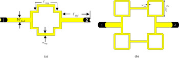
Figure 1 shows the proposed structure of the new filter topology. The target is to achieve the switchable BPF-to-BSF responses with separately tuned electronic semiconductor device. The substrate Duroid Rogers RO5880 is used as a platform with dielectric thickness h = 0.787 mm, relative effective dielectric constant ε eff = 2.2, loss tangent δ = 0.0009, and copper thickness t = 0.0017 mm. The ground plane of this filter completely occupies the back face of that substrate. The filter structure consists of a main ring resonator with a side length ℓ ring = 11.8 mm, which is equivalent to (≈λ g /2) at the center frequency of 11 GHz, with a line width w ring = 0.64 mm. Every side is folded from its ends up to ≈λ g /8 and then connected to the other sides. Finally, the main ring resonator is shown in Fig. 1(a).
(a) The main ring resonator structure, (b) series-shunt ring resonator structure.

The corners have been completed to become four small square ring resonators as shown in Fig. 1(b). Each side of the small square ring resonator measures ℓ pad = 5.8 mm, that is equivalent to (≈λ g /4), with line width w pad = 0.64 mm at a resonance frequency of 11 GHz calculated based on equation (1).
 $$f_0 = \displaystyle{{nc} \over {\lambda _g \sqrt {\varepsilon _{eff}}}}, $$
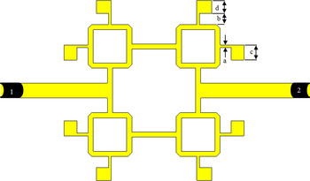
where f 0 is the center frequency, n is the number of modes, c is the speed of light, λ g is the guided wavelength and ε eff is the effective dielectric constant. In addition, two-step impedance tuning open stubs were merged at θ = ∓45° and θ = ∓135° at all ring resonators, as shown in Fig. 2 with the parameters a = 0.35 mm, b = d = 1.5 mm, and c = 2.5 mm, to obtain a broader BPF.
The proposed microstrip BPF structure.

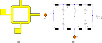
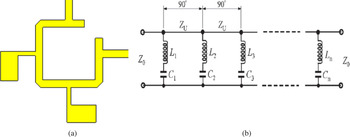
The ring circuit consists of a combination of duo perturbed circuits, represented by two tuning stubs loaded on the ring resonator to achieve a wide passband with a sharp cutoff characteristic. This method can be explained as using two stopbands that are generated by two tuning stubs in conjunction with the wide passband. For more clarity, Figs 3(a) and 3(b) represents the circuit model of one ring resonator.
Circuit model of one ring resonator for BPF applications.

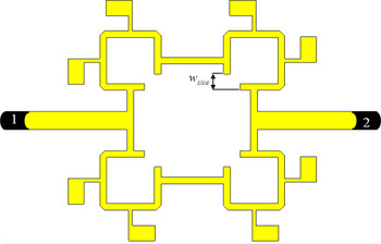
The input/output feed lines, with characteristic impedances of 50 Ω were directly coupled to the main ring resonator, as a symmetric state, to reduce radiation and mismatch losses [Reference Hsieh and Chang11]. The width of feed lines is w fed = 1.79 mm. A gap w sice = 1.25 mm was made opposite to the corner, between the step impedance tuned open stubs in each resonator, as shown in Fig. 4. This gap represents a key point of the proposed filter to provide the stopband characteristic with a similar center frequency and bandwidth.
The proposed microstrip BSF structure.

Bandstop characteristic was achieved because each ring resonator—after cutting—resembled a transmission line electrically coupled to the quarter wavelength open stub resonators, which were spaced by a quarter-guided wavelength apart. For more clarity, Figs 5(a) and 5(b) represents the circuit model of one ring resonator.
Circuit model of one ring resonator for BSF applications.

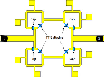
PIN diodes types HMPP3890 were connected to the terminals of these gaps to achieve switchable BPF-to-BSF characteristics (http://www.avagotech.com/pages/en/rf_microwave/diodes/pin/hmpp-3890/). In this regard, PIN diode acts as a switchable on-off key that can be either open or short to exhibit the desired response. All diodes were modeled using a full-wave electromagnetic simulation (computer simulation technology (CST) Microwave Studio, 2010) [12]. As in the practical case, PIN diodes will operate either in forward or reverse bias, as clearly shown in Fig. 6. To eliminate the possibility of a short circuit at the PIN diode and DC power supply, a DC blocking microstrip capacitor (cap) was used, as shown in Fig. 6.
The proposed switchable filter with embedded PIN diode and DC blocking capacitor.

III. SWITCHABLE BPF-TO-BSF BEHAVIOR
The main ring resonator shown in Fig. 1(a) has been modeled using CST Microwave Studio. The current distributions and the resulting response of the proposed ring resonator are shown in Figs 7 and 8, respectively. Preliminary results of the S-parameters and surface current distributions clearly illustrate the bandpass characteristic with resonant pole frequencies in the UWB.
Surface current distribution of the main ring resonator.

Simulated S-parameters of the main ring resonator.

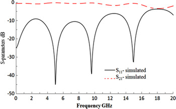
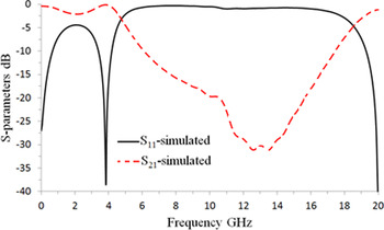
The corners of the main ring resonator were completed to form four square ring resonators, as shown in Fig. 1(b). This setup shows that every two-ring resonators connected in series and parallel obtain a wider bandwidth. The side length of each square ring was designed to be equal to (≈λ g /4). The resulting response of the new configuration reflects UWB-stop characteristics shown in Fig. 9, as demonstrated in [Reference Chang13].
Simulated results of the series-shunt square ring resonators.

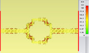
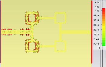
The results shown in Fig. 10 imply that the surface current distributions of the series-shunt square rings has exhibited the bandstop characteristics of the filter because of the orthogonality of the line side of the main ring to the small square rings [Reference Hsu, Chen and Huang1, Reference Hsieh and Chang11]. Thus, these lines were considered as input/output feed lines for each small square ring. In addition, the bandstop characteristics were realized because of the zero electric current in the output line. In other words, the odd mode was excited and caused short circuit [Reference Hsu, Chen and Huang1, Reference Hsieh and Chang11].
Surface current distributions of series-shunt square ring resonators.

Referring to Fig. 1(b), two-step impedance tuned open stubs were added in the free small ring sides at θ = ∓45° and θ = ∓135° to obtain the bandpass characteristics. This has been presented in [Reference Hsieh and Chang11, Reference Hong and Lancaster14] and also shown in Fig. 2. Figure 11 represents the response of UWB-pass filter related to the BPF structure illustrated in Fig. 2. The simulated results show substantial bandwidth of 70.11%, insertion loss of 0.3 dB, three transmission zeros at (f z1 = 6.75 GHz, f z2 = 15.6 GHz, and f z3 = 17.25 GHz) with stopband of more than 2 GHz with rejection 35 dB. The return loss is more than 18 dB with six transmission poles. In addition, the new design has many features; a compact size, improved fractional bandwidth, reasonable return loss, low insertion loss, and wide stopband. All these characteristics meet the requirements of the UWB systems [Reference Ma, Cai, Guan, Kobayashi and Anada15].
Simulated results of the proposed microstrip BPF.

Although the outcomes have shown good results, the design did not achieve the desired goal. In addition, this structure displays only one characteristic (i.e. UWB BPF). For this reason, Fig. 2 was upgraded to a new configuration by cutting the corners of each small ring resonator, as depicted in Fig. 4. These gaps were created to transfer the response from bandpass-to-bandstop characteristic, as shown in Fig. 12. The bandstop characteristic was excited since each ring resonator, after gap creation, resembles as a transmission line that is electrically coupled to the quarter wavelength open stub resonators, the open stub resonators are separated a quarter-guided wavelength away from each other [Reference Chang13, Reference Hong and Lancaster14]. Furthermore, each open stub will resonate at a different frequency which in turn leads to the appearance of many transmission poles.
Simulated results of the upgraded microstrip BSF.

In accordance to Figs 11 and 12, both the bandpass and bandstop responses can be achieved using two different configurations. In other words, short and open circuit in each small ring resonator made the difference between these two configurations. The primary objective was to find a suitable design that can be used to obtain both responses within same construction. An appropriate electronic element was needed to get a short and open circuit to realize these structures (i.e. Figs 2 and 4) in the same setup. Therefore, the switching PIN diode was used, as shown in Fig. 6, to perform this function and to obtain switchable filter with both bandpass and bandstop responses.
IV. ELECTRONICALLY SWITCHABLE FILTER RESULTS AND DISCUSSION
The proposed filter structure, illustrated in Fig. 2, was modeled and analyzed at a design frequency of 11 GHz using CST Microwave Studio and taking into account the dielectric and metallic losses. The conductivity of copper σ = 5.8 × 10⁷ S/m and the substrate loss tangent δ = 0.0009 were used in the simulation. At the resonance frequency, the small square ring side length was set to 5.8 mm that is equivalent to a quarter guided wavelength λ g .
Tunable step impedance open stub resonator, with estimated dimensions as shown in Fig. 2 and overall length equivalent to quarter guided wavelength, was merged to the free sides of each small square ring resonator. The proposed microstrip BPF was fabricated on a substrate with a relative dielectric constant of 2.2 and a thickness of 0.787 mm. A standard technology printed circuit board (PCB), and the sub miniature version A (SMA) connector was attached at the input/output feed lines.
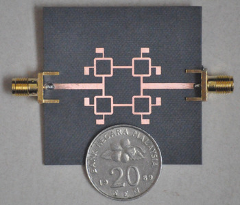
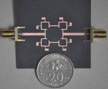
Figure 13 shows a photograph of the fabricated BPF structure design with the specified dimensions depicted in Fig. 2. The total size of the proposed filter is 23 × 23 mm2. In addition, the new model has shown the possibility of obtaining UWB characteristics, as well as reasonable return and transmission loss characteristics. However, this is at odds to the claims by the authors in [Reference Jong, Chew, Leong and Ooi16, Reference Lee, Cho and Yun17]. One of the cited literatures has shown wide bandwidth by connecting three series square ring resonators [Reference Hsieh and Chang11]. However, the obtained bandwidth is not compatible with the achieved result in this study shown in Fig. 14.
A photograph of the fabricated proposed BPF prototype.

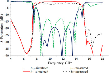
Simulated and measured results of the proposed BPF.

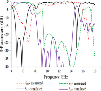
Figure 14 shows the simulated and measured results of the proposed BPF in terms of transmission and reflection characteristics. The measurements were conducted in an ordinary room environment by vector network analyzer, (VNA model: Anritsu37347D). The results show that the simulated and measured responses were in good agreement with each other and thus validate the design process. The fabricated BPF offers many features; three transmission zeros (f z1 = 6.75 GHz, f z2 = 15.67 GHz, andf z3 = 16.68 GHz) and six transmission poles. It also has a fractional bandwidth of 69.227% at 3 dB with wide stopband characteristics on both sides of more than 2 GHz. The obtained roll-off was with sharp responses of 81.533 and 81.47 GHz/dB. Such responses illustrate the BPF high selectivity in the transmission band. The results exhibit a good performance of S 21 of less than 1.5 dB within the transmission band from 11.225 GHz up to 14.533 GHz. However, S 21 has degraded at the lower and upper transmission bands reaching 3.35 dB. The return loss has better than 12 dB across the passband from 8.528 to 14.561 GHz. The S 11 response featured smallest value at the lower and upper passband up to 5 dB.
As mentioned earlier, a small gap w sice has been created to get a BSF, as shown in Fig. 4. The microstrip BSF structure was practically fabricated on a PCB using a Duroid Rogers's substrate, as shown in Fig. 15. The same design parameters were used as depicted in Fig. 2. In other words, the BPF was recalled once again. However, a small aperture was engraved in all small resonator corners opposite to the corner in between the step impedance open stubs to be the key point of this design. These apertures were designed with dimensions less than that of the selected PIN diode in order to fix it on the aperture sides. A full ground plane covers the backside of the substrate, which means that no additional structures were added to obtain the presented results. The proposed filter was designed with lower complexity and to be cost effective as compared with liquid crystal polymer and low temperature co-fired ceramic [Reference Hao and Hong18, Reference Chien, Shen, Huang, Wang and Wu19].
A photograph of the proposed BSF prototype.

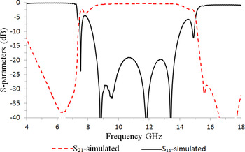
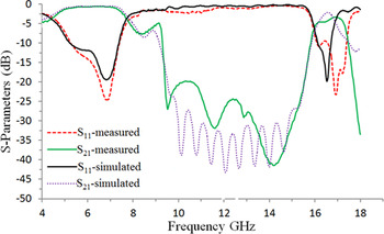
Both simulated and measured results were compared in terms of return loss and transmission responses, as shown in Fig. 16. The results clearly reflect the compatibility between the simulated and measured results. In addition, the BSF almost resonates at the same center frequency and bandwidth, as compared with that of the BPF (11 GHz). Furthermore, the return loss response with ripple value of 1.5 dB in most of the band featured three transmission zeros (f z1 = 6.372 GHz, f z2 = 16.203 GHz and f z3 = 16.957 GHz). The rejection band of the lower band is better than the upper band, which are 1.6 and 0.756 GHz at 10 dB, respectively. Five transmission poles occur at 7.3, 8.83, 10.62, 12.45, and 14 GHz. However, slight variation of 1.8 dB was noticed in the lower band between the simulated and measured results. This deviation can be attributed to the fabrication tolerance and mismatching between the SMA connectors and the feed lines. In comparison with the responses of recent literature, the proposed structure offers a compact size of about 54.12 and 89.5% when compared with the works reported in [Reference Mansour, Hall, Gardner and Abd Rahim20, Reference Sorkherizi, Kishk and Khaleghi21] respectively. In addition, it shows good characteristics in terms of size, response, and selectivity.
Simulated and measured results of the proposed BSF.

A) Forward bias of PIN diode
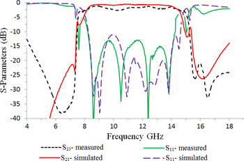
As demonstrated in Fig. 6, all PIN diodes were connected to the terminals of the gap. Applying forward DC bias to all PIN diodes will entail all diodes to function as ON (short circuit). In other words, a small resistive value was added to the model of the PIN diode resembling the ON state. A BPF response of the new proposed structure was tested using the CST Microwave Studio. The possibilities of the laboratory prevented us from installing the PIN diode inside the structure because this type of PIN diode required high quality of operating machine. Thus, the simulated results were compared with the practical results related to Fig. 14. Figure 17 illustrates the return loss and transmission responses of the modeled structure of Fig. 6 using PIN diode and the measured results of Fig. 14 of the BPF. The simulated and the measured results were in good agreement with each other, thus validating the proposed filter structure. Some degradation in performance was shown due to PIN diode parasitic resistance that will result in power loss so that total efficiency will be reduced.
Comparison of the measured results and simulated results of the proposed BPF structure using PIN diode to validate the switchable filter.

B) Reverse bias of PIN diode
A negative DC voltage was applied to reverse bias all the PIN diodes thus representing open circuit. The simulated results were obtained and then were compared with the measured results of Fig. 16. As shown in Fig. 15, the gap of each small ring resonator was similar to the case of the applied voltage for all PIN diodes were negative, and the reverse bias can take place. In this case, the higher resistance due to the parallel connection of small capacitance and resistance in the PIN diode led to it being in the OFF state. In this context, the PIN diodes resemble open circuit or OFF to represent the gap as presented in Fig. 15. A DC microstrip capacitor was used and fixed inside the structure as presented in Fig. 6. To avoid the DC short circuit that may happen between the PIN diode and DC power supply.
Figure 18 shows the simulated result of the structure illustrated in Fig. 6, all PIN diodes in reverse bias states, with the measured results obtained from Fig. 16. Both the return loss and the transmission responses of the simulated and the measured results of the PIN diodes were close to each other. However, the observed frequency shift around 0.87 GHz between the simulated and measured is attributed to the PIN diode parasitic characteristic that is inevitable.
Comparison of the measured results BSF and simulated results of the proposed structure using PIN diode to validate the switchable filter.

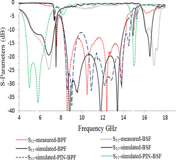
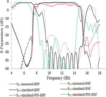
The measured and simulated S 11 and S 21 of the three presented structures are summarized in Figs 19 and 20, respectively.
Comparison of the simulated and measured S 11.

Comparisons of the simulated and measured S 21.

V. CONCLUSIONS
A new switchable bandpass-to-bandstop UWB filter was designed in this paper. With a simple series-shunt square ring resonator with quarter wavelength, open stub resonators were merged into one structure to validate the proposed idea. In other words, a closed square ring resonator, as series-shunt configuration, is connected to offer the BPF. By creating a gap in each resonator, a bandstop response following the simple transmission line with the open circuited stub was obtained. Simulated and measured results showed that the presented microstrip filter offers a switchable response from bandpass-to-bandstop characteristic.
The measured results of the BPF prototype exhibited three transmission zeros (f z1 = 6.75 GHz, f z2 = 15.67 GHz, and f z3 = 16.68 GHz), and six transmission poles. The prototype also has a rejection bandwidth of more than 2 GHz and an insertion loss of 1.5 dB within the transmission band from 11.225 to 14.533 GHz. Moreover, it has a fractional bandwidth of 69.227% at3 dB with a roll-off response of 80.764 and 81.533 GHz/dB for the BPF skirt. This response allows the proposed filter to be high in selectivity in the transmission band. The BSF prototype shows three transmission zeros (f z1 = 6.372 GHz, f z2 = 16.203 GHz, and f z3 = 16.957 GHz) and a return loss response with ripple value of 1.5 dB in the band. Five transmission poles happened at 7.3, 8.83, 10.62, 12.45, and 14 GHz. Finally, the rejection of the lower band is better than that of the upper band, which is 1.6 and 0.756 GHz at 10 dB, respectively. Measured results have been carried out on both filter prototypes to validate the reality of simulated results.
ACKNOWLEDGEMENTS
The authors would like to thank the Center for Radiofrequency and Microwave Engineering, University Tenaga Nasional for its financial support for the research. Also, they would like to express their thanks to the head of Microwave Research Group, University of Technology, Iraq for the valuable discussions and support, and also wish to thank the reviewers for their useful and constructive comments.
 Mushtaq Alqaisy was born in Baghdad, Iraq in June of 1971. He received his B.Sc. and M.Sc. degrees in Electrical Engineering/Communication Engineering from Al-Rasheed College for Science and Technology, Iraq in 1996 and 2005, respectively. He is currently working towards his Ph.D. degree in Microwave Communication Engineering in the faculty of graduated study, Tenaga National University. His research interests include the analysis and design of microwave passive circuits. He is a student Member of IEEE.
 Chandan Kumar Chakrabarty was born in Malaysia. He received his B.Sc. (Hon) Physics in 1986 and M.Sc., Major in Plasma Physics in 1989 from University of Malaya and Ph.D. in Radiofrequency Plasma in 1996 from Flinders University of South Australia. He is currently involved in the research of developing ultra-wideband antennas for partial discharge detections in MV and HV underground cables, meta-materials microwave antenna and filters, and FPGA based partial discharge location and detection system for power distribution assets. He is currently a Professor in the Electronics and Communications Engineering Department at University Tenaga Nasional and also the head of the research center for radiofrequency and microwave engineering.
 Jawad Kadhim Ali was born in Baghdad, Iraq in November of 1956. He received his B.Sc. and M.Sc. degrees in 1979 and 1986, respectively, from Al-Rasheed College for Science and Technology, Iraq. From 1989–1991, he joined the Ph.D. study program at AZMA Academy, Brno, former Czechoslovakia. Since 2010, he has been a Professor of Microwave Engineering at the University of Technology, Iraq. He is the founder and head of Microwave Research Group at the Department of Electrical Engineering. Currently, he is the deputy dean for postgraduate studies and scientific affairs at the Department of Electrical Engineering. His fields of interests are microwave antenna miniaturization and design, and passive microwave circuits design. He has more than 100 published papers in local and international conferences and peer-reviewed journals. Prof. Ali is a Senior Member of IEEE and member of IET and IEICE.
 A. R. H. Alhawari was born in Jordan. He acquired his B.Sc. degree in Communication Engineering from Hijjawi Faculty for Engineering Technology of Yarmouk University, Jordan in 2003. During his B.Sc. he had done an internship program for couple of months in Cairo, Egypt for Industrial Training. Meanwhile the MSc. and the Ph.D. degrees were both pursued later in 2009 and 2012, respectively, in Wireless Communications Engineering from Universiti Putra Malaysia, Malaysia. That was after a double 2-year duration working in Jordan and then Saudi Arabia. Currently, he is a senior lecturer at the Department of Computer and Communication Systems Engineering, Universiti Putra Malaysia since December, 2012. His main research interests are in metamaterial antennas, microwave absorbers, and RFID.
 Tale Saeidi was born in Mashhad, Iran, in 1985. He received his B.Sc. degree (2008) in Engineering from Khayam University of Mashhad, Engineering Department. In 2009, he began a M.Sc. degree at Universiti Putra Malaysia (UPM), Wireless Communication Engineering Department. His areas of interest include, microwave engineering; antenna and propagations; and phased array radars. He has published many papers relating to these fields.