Introduction
The development of transmission/reception (T/R) components in wireless communication systems is inseparable from the rise of II–-V semiconductors [Reference Liang, Tang, Zhao, Xie and Geng1, Reference Jin, Wan, Tao, Huang and Wu2]. Low-noise amplifiers (LNAs), as essential component of wireless receiving systems, are vital for improving the signal transmission quality of communication systems [Reference Liang, Tang, Zhao, Xie and Geng1–Reference Li and Serdijn5]. As a result, driven by application requirements, achieving bandwidth expansion and a more compact chip size of the LNA monolithic microwave integrated circuit (MMIC), as well as reducing power loss, has become the most promising research topic at present [Reference Liang, Tang, Zhao, Xie and Geng1–Reference Li and Serdijn5].
In recent years, various technologies have been proposed to promote the performance of LNA MMIC, such as current-reused construction [Reference Liang, Tang, Zhao, Xie and Geng1, Reference Jin, Wan, Tao, Huang and Wu2, Reference Zhang, Qian, Zhong and Liu6–Reference Lei, Wang, Chiong and Wang13] negative feedback networks (NFNs) [Reference Cai, Lu, Tan, Wu and Yu3, Reference Chen and Lin4, Reference Liu, Wang and Xu7, Reference Hu, Ma, Mou and Meng14], and reconfigurable techniques [Reference Xie, Yu and Tan15]. Specifically, as shown in reference [Reference Hu, Ma, Mou and Meng14], an LNA MMIC operating at 0.1–20 GHz is presented by using feedback techniques, achieving a noise figure (NF) of 3.1–5.8 dB, an output 1 dB compression point (OP1 dB) of 7.8–12.7 dBm, and a power consumption of 505 mW. In reference [Reference Xie, Yu and Tan15], based on reconfigurable technology, an LNA MMIC working at 12–20 GHz is presented, occupying a chip area of 2 × 1.8 mm2, achieving an OP1 dB of 2.2–5 dBm, and a power consumption of 227.5 mW. As a result, it can be seen that these reported works demonstrate some technological advantages in promoting certain performance of LNA. However, as is well known, many technical indicators of LNA, such as operating bandwidth, OP1 dB, power loss, NF and chip area, have a trade-off pattern, meaning that in practical engineering applications, these technical indicators need to be at an acceptable level, which is extremely important for the engineering design of LNA.
In this letter, an ultra-wideband (UWB) LNA MMIC operating in the S-C-X-Ku band is presented by employing current-reuse construction. Meanwhile, an NFN and source adaptive bias circuit are used to achieve bandwidth expansion and the compact chip size of the proposed LAN MMIC. Subsequently, theoretical verification is carried out based on a 0.15-µm gallium arsenide (GaAs) pseudomorphic high-electron-mobility transistor (pHEMT) process. The measured results demonstrate the effectiveness of the proposed design method.
UWB LNA MMIC circuit topology and design
The proposed UWB LNA MMIC design is implemented using the 0.15 µm GaAs pHEMT technology of Sanan Semiconductor. In order to balance the size, power consumption, and gain of the chip, a current-reuse topology is adopted, where the two transistors M1 and M2 have the same size, which is 4 × 45 µm. Based on this, the proposed LNA schematic is presented in Fig. 1, which includes two NFNs, a source adaptive bias circuit, and a current-reuse construction. All parameter values in the circuit are given as shown in Table 1.
Circuit schematic of the proposed UWB LNA MMIC.

Parameters of the proposed UWBLNA MMIC (UNIT: L, nH; R, Ohm; C, pF; TRANSMISSION LINE-W/L, µm/µm; M, µm2)

Para: Parameter.
As demonstrated in Fig. 1, the transmission path guided by the red dashed line with the drain current I d is the direct-current (dc) path of the proposed LNA. The circuit located in the orange shaded area is the current-reuse construction used, where transistors M1 and M2 share the same drain supply, which can effectively reduce the power loss of LNA MMIC. The transmission path guided by the blue dotted line with the radio frequency (RF) mark is the RF path of the proposed LNA, in which the inductor L 2 is used to prevent the RF signal from leaking into the dc path, and similarly, the capacitor C7 is used to prevent the dc signal from entering the RF path.
The gate bias voltage (−0.5 V) of the first stage is generated by the drain current of transistor M2 acting on the resistor R7 in the adaptive bias network, which can eliminate the design of the gate bias network of transistor M1, weaken the design complexity of the dc power supply network, and help reduce the overall size of the chip. In addition, the adaptive bias network RC located at the source of transistor M1 combined with microstrip line T2 can form source stage feedback to achieve bandwidth expansion, specifically manifested in the capacitive reactance decreases with increasing frequency, which helps to compensate for the inherent gain roll-off of the transistor [Reference Razavi16]. The gate bias voltage of the second stage transistor M2 is provided by a resistive voltage divider network composed of R5 and R6, which also helps to reduce the design complexity of the dc power supply network. In addition, the resistor voltage divider network composed of R5 and R6 is also used to promote the OP1 dB of LNA, which is mainly achieved by manipulating the drain source voltage (Vds1 and Vds2) distribution of transistors M1 and M2 using the ratio of R5 and R6. For this design, the OP1 dB of LNA is determined by the second stage transistor M2, while for the current-reused structure, the drain current (I ds) of the two stage transistors is the same. Therefore, increasing the output power of the second stage can be achieved by increasing the drain source voltage Vds2 of M2.
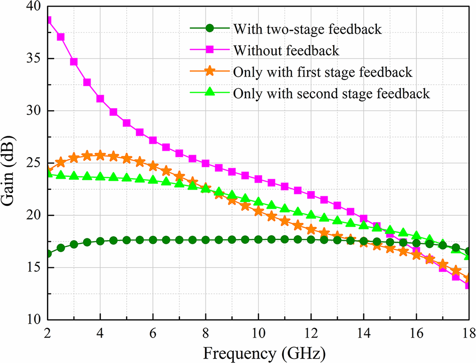
Moreover, in order to compensate for the inherent gain roll-off characteristics of transistors, feedback techniques are also introduced into the proposed LNA MMIC circuit design. As a result, a NFN composed of R-L-C is employed in the two stages of the proposed LNA to achieve bandwidth expansion, as exhibited in Fig. 1. Figure 2 demonstrates the simulated gain curves with and without NFNs for the proposed LNA MMIC, where C3 and C5 are used to isolate dc from the gate and drain stages of transistors M1 and M2. As displayed in the simulation results in Fig. 2, it can be seen that the LNA MMIC without the addition of NFN exhibits a more obvious gain roll-off characteristic. Compared to introducing feedback circuit only in the first or second stage, the bandwidth expansion effect generated by introducing R-L-C NFN in both stages of amplification topology is more obvious through compensating for the gain roll-off of the transistor.
Simulated gain curves with and without NFNs for the proposed LNA MMIC.

To verify the conversion performance of the input impedance and output impedance to 50Ω completed by the input matching network of the first stage and the output matching network of the second stage of the topology network presented in Fig. 1, the simulated impedance trajectories of the input and output terminals of the proposed LNA MMIC are plotted in Fig. 3, where the orange solid line represents the input terminal and the green dashed line represents the output terminal. As exhibited in the figure, the impedance completed at both the input and output terminals varies closely around the 50Ω at the center of the Smith chart, indicating the rationality of the matching network design.
The simulated impedance trajectory variation of the input and output of the proposed LNA MMIC in 2–18 GHz.

Simulated and measured results
As a validation of the proposed design method, a prototype is designed, fabricated, and measured using a 0.15-µm GaAs pHEMT process. Figure 4 demonstrates a photograph of the proposed UWB LNA MMIC with a chip area of 1.2 × 1.5 mm2. The measured LNA consumes a 44-mA dc current from a 5-V dc supply, which generates a 220-mW dc consumption.
Chip microphotograph of the proposed UWB LNA.

Subsequently, the small signal measurement is executed, and the measured results for the S-parameter are plotted in Fig. 5(a). As displayed in the figure, it can be seen that within the target frequency band of 2–18 GHz, the proposed LNA MMIC achieves S21 between 15.5 and 17.8 dB, while S11 and S22 are maintained below −16.3 and −14.5 dB, respectively. Furthermore, the voltage-standing-wave ratio (VSWR) at the input of the measured LNA MMIC is presented in Fig. 5(b). As exhibited in the figure, the implemented VSWR is between 1.127 and 1.35 in the entire S-C-X-Ku-band. Meanwhile, Fig. 5(c) demonstrates that the measured OP1 dB is 15 ± 0.5 dBm for V D = 5 V over the 2–18 GHz.
Simulated and measured results of small-signal. (a) S-parameter. (b) VSWR. (c) OP1 dB.

The NF measurement of the fabricated LNA MMIC is performed, and the simulated and tested results are exhibited in Fig. 6, where the measured NF is between 3 and 3.65 dB from 2 to 18 GHz. It should be noted that the lack of outstanding NF performance of the proposed LNA is mainly attributed to two aspects. First, in the target frequency band of 2–18 GHz, in order to balance the NF performance in the high-frequency band, it is necessary to sacrifice the noise performance in the low-frequency band to ensure that the NF of the entire design frequency band is at an acceptable level. The second is that 1/f noise within the entire design frequency band can also have a significant impact on the NF of LNA.
Measured result of NF from 2–18 GHz.

Besides, the measured the input third-order intercept point (IIP3) of LNA in the target frequency band range of 2–18 GHz using a two-tone signal with an interval of 1 MHz and an input power of 5 dBm, is shown in the Fig. 7. It can be seen that within the target frequency band, the proposed LNA MMIC achieves IIP3 between 9.8 and 11.6 dBm.
Measured IIP3 of the designed amplifier against frequency.

Based on reference [Reference Zhang, Wang, Yan and Liang21], a modified figure of merit (FOM) considering the center frequency, bandwidth, gain, NF, dc power, and OP1 dB, is adopted to conduct a state-of-the-art comparison as follows [Reference Zhang, Wang, Yan and Liang21]:
 \begin{align}FOM = 20\log {}_{10}\left( {\frac{{Gain\left[ {abs} \right] \cdot O{P_{1dB}}\left[ {mW} \right]}}{{\left( {N{F_{\min }}\left[ {abs} \right] - 1} \right) \cdot {P_{dc}}\left[ {mW} \right]}} \cdot \frac{{BW\left[ {GHz} \right]}}{{{f_0}\left[ {GHz} \right]}}} \right)\nonumber\\ \end{align}
where f 0 is the center frequency. As a result, a comparison between the proposed LNA MMIC and other published LNA MMICs is presented in Table 2. By comparing the performance parameters in the table, it can be concluded that the implemented LNA demonstrates a comprehensive technical advantage.
Comparisons with state-of-the-art integrated LNA MMIC

# Estimated value from the figure.
Conclusion
An UWB current-reused LNA MMIC with two-stage cascading is presented in this letter for wireless communication. A NFN and source adaptive bias circuit are introduced to achieve bandwidth expansion and compact chip size for the proposed LAN MMIC. The proposed design scheme has been validated by fabricating the LNA in 0.15-µm GaAs pHEMT technology, which occupies a chip area of 1.2 × 1.5 mm2. The measured results manifest that the proposed LNA achieves a small signal gain of 15.5–17.8 dB, a NF of 3–3.65 dB, and an OP1 dB of 14.5–15.5 dBm from the target bandwidth of 2–18 GHz, indicating potential commercial value in wireless communication.
Data availability statement
Data sharing not applicable to this article as no datasets were generated or analyzed during the current study.
Acknowledgement
The work proposed by Project of Zhejiang Provincial Science and Technology plan (Grant 2024C01076), Shanxi Provincial Science and Technology plan (Grant 2023ZDLGY49), National Key R&D Program of China (Grant 2018YFE0207500), Project of Ministry of Science and Technology (Grant D20011), the National Natural Science Foundation (Grant 62201181), University Natural Science Foundation of Anhui Province (Grant No.2022AH051578), Anhui Province Key Laboratory of Simulation and Design for Electronic Information System (2023ZDSYS09).
Author contributions
Xuefei Xuan and Tingwei Gong.
Competing interest
The authors declare that they have no known competing financial interests or personal relationships that could have appeared to influence the work reported in this paper.

Xuefei Xuan received the M.E. degree in electromagnetic field and microwave techniques from Hangzhou Dianzi University, Hangzhou, Zhejiang, China, in 2018, where he is currently pursuing the Ph.D. degree. He is currently with Dublin City University, Dublin, Ireland, as a Visiting Student. His research interests include design of RF/mm-wave power amplifiers, efficiency enhancement techniques, broadband techniques, and mm-wave integration circuits and systems.

Zhiqun Cheng (Member, IEEE) received the B.S. and M.S. degrees from the Hefei University of Technology, Hefei, China, in 1986 and 1995, respectively, and the Ph.D. degree in microelectronics and solid state electronics from the Shanghai Institute of Metallurgy, Chinese Academy of Sciences, Shanghai, China, in 2000.
From 1986 to 1997, he was a Teaching Assistant and a Lecturer with the Hefei University of Technology, China. From 2000 to 2005, he was an Associate Professor with the Shanghai Institute of Metallurgy, China. He is currently a Professor and the Dean of the School of Electronic and Information, Hangzhou Dianzi University. He has authored or co-authored over 150 technical journal and conference papers. His research interests include microwave theory and technology, MMIC, power amplifier, and RF front end. He is currently a member of a Council of Zhejiang Electronic Society. He was also a Chair of the Organizational Committee for over 10 International Conferences.

Tinwei Gong is currently pursuing the Ph.D. degree with Hangzhou Dianzi University, Hangzhou, China.
His research interests include the design of RF/mm-wave power amplifiers, efficiency enhancement techniques, broadband techniques, and mm-wave integration circuits and systems.

Zhiwei Zhang received the B.S. degree in electronic science and technology from Hangzhou Dianzi University, Hangzhou, China, in 2017 and the Ph.D. degree in electronic science and technology from the Hangzhou Dianzi University (HDU), Hangzhou, China, in 2022.
He is currently an Associate Professor with HDU. His current research interests include highly linear and efficient microwave PA design.

Chao Le he is currently the project leader of Fuyang Electronic Information Research Institute Co., Ltd. of Hangzhou Dianzi University (HDU).