Introduction
Interface conduction and the exemplary LaAlO3/SrTiO3 two-dimensional electron gas/liquid
It is in use as artificial diamond, but for many scientists, it has the appeal of a complete jewelry shop: Strontium-titanate, SrTiO3, the perovskite crystal structure that looks deceptively simple, but which harbors tremendously rich physics, especially when electronically doped. In 1969, Marvin Cohen, the co-discoverer of superconductivity in oxygen-reduced SrTiO3, Reference Schooley, Hosler and Cohen1 said, “If SrTiO3 had magnetic properties, a complete study of this material would require a thorough knowledge of all of solid state physics.” Reference Cohen, Parks and Dekker2 In their 1987 Physics Nobel lecture, J. Georg Bednorz and K. Alex Müller mention SrTiO3 together with LaAlO3 as key materials under study, leading to the discovery of high-temperature superconductivity in cuprate perovskites. Reference Bednorz and Müller3 Notably, these two electrically insulating materials marked the beginning, in 2004, of a new chapter in the research on oxides, now focusing on their interfaces. Akira Ohtomo and Harold Y. Hwang showed that the contact area between a LaAlO3 film and a SrTiO3 substrate, of which the top-most atomic layer was chemically prepared to be TiO2, is conducting. Reference Ohtomo and Hwang4 Meanwhile, many additional remarkable properties have been observed for the LaAlO3/SrTiO3 interface, and these even include magnetic effects. In addition, this field of research has expanded to include many other oxide interface combinations.
These developments raise the questions: What makes these oxide interfaces so special, and what could they have further in store? Before turning to these questions, it is useful to note that among scientists working in the field of oxide electronics, a distinction is made between “simple” and “complex” oxides. The former includes such materials as SiO2, TiO2, and ZnO, which have many interesting and useful properties—not really simple, by the way. Especially noteworthy in relation to interface conductance is research on two-dimensional electron gases (2DEGs) at the interface between ZnO and MgZnO, in which electron mobilities up to 700,000 cm2/Vs at temperatures below 1K have been reached. Reference Kozuka, Teraoka, Falson, Oiwa, Tsukazaki, Tarucha and Kawasaki5 The observation of the fractional quantum Hall effect in these systems, requiring ultra-low defect densities, exemplifies the excellent quality of these interfaces. In many respects, the ZnO/MgZnO interfaces can be viewed as an oxide analogue to semiconductor 2DEGs such as GaAs/AlGaAs with potentially very long spin coherence, of interest for spintronic (quantum) devices. Reference Kozuka, Teraoka, Falson, Oiwa, Tsukazaki, Tarucha and Kawasaki5
The designation of “complex” oxides is used for materials comprising—next to the oxygen anion—two or more cationic elements. Canonical examples of these are the perovskite oxides with the generic crystal unit cell composition ABO3, in which A is typically an element from the alkaline earth or rare-earth metal groups, and B is a (post-)transition metal element (Ti, V, Mn, Fe, Cu, Ru, Ir, Al, Bi). In their stoichiometric “parent compound” phase, many of the perovskites are insulating, either in the form of standard band insulators, as is the case for SrTiO3 and LaAlO3, or in the form of Mott insulators, such as LaTiO3. The “Mottness” is a specialty of materials in which charges at the Fermi energy are loosely bound to a sublattice of ions, in principle able to hop between sites. For the case of half filling, meaning that all available states are occupied by one electron with either spin up or spin down, a conductance deadlock occurs, and the Mott-insulating state arises. Magnetic and electron-lattice interactions can give rise to various forms of spin and orbital ordering in this insulating state.
For the Mott insulators, p and n doping are both possible by shifting the chemical potential away from the half filling state using chemical substitution or electrostatic gating. This doping breaks the conductance deadlock, giving rise to an insulator-to-metal transition. For the band insulators, p doping is often counteracted by the creation of oxygen vacancies, making it difficult to create p-type oxide conductors. Electron doping, however, can be accomplished quite straightforwardly. For example, in the previously mentioned SrTiO3, replacing part of the Ti4+ ions with Nb5+ or creating oxygen deficiency by annealing in a vacuum provides mobile electrons that fill a Ti 3d-derived conduction band. Reference Imada, Fuijimori and Tokura6 The conducting states of complex oxides are very tantalizing, resulting from the strong and local interplay between the charge, spin, orbital, and lattice degrees of freedom. Many special phenomena occur, such as steep metal-to-insulator transitions, non-Fermi liquid behavior, (high-T c) superconductivity, and colossal magnetoresistance. Reference Imada, Fuijimori and Tokura6
Interfacing with other materials presents an alternative way of donating charge to the stoichiometric parent compound. The creation of a confining potential at interfaces, resulting, for example, from work function differences or from Fermi-level pinning by surface states, is a well-known phenomenon. These confining potentials become filled with electrons, provided by, for instance, diffusion from the adjacent materials when these are conductors or Mott insulators, by cation impurities or oxygen vacancies, by photo-excitation, or by electric field gating. These electrons can be delocalized along the interface, giving rise to a 2DEG.
An additional mechanism for charge transfer can be at play in particular oxide materials combinations, for which a discontinuity in the internal polarization state of the material arises at the interface. This has been suggested as a key mechanism in the case of SrTiO3/LaAlO3. Reference Nakagawa, Hwang and Muller7 In these respective materials, the Sr2+O2– and Ti4+(O2–)2 layers are in first approximation charge neutral, whereas the adjacent La3+O2– and Al3+(O2–)2 layers present a polar system. When growing a thin film of LaAlO3 on a SrTiO3 substrate chemically prepared to have only one type of atomic layer at the surface, such as TiO2 which selects the film to start with a LaO layer, an electrostatic potential build-up occurs inside the LaAlO3. Before this potential build-up can reach unphysically high values with increasing LaAlO3 layer thickness, denoted as the “polar catastrophe,” compensating mechanisms such as structural reconstructions or charge transfer from the LaAlO3 surface to the SrTiO3/LaAlO3 interface will set in. The latter is referred to as “electronic reconstruction,” a term first coined in the context of polar discontinuities/polar surfaces for the case of K3C60. Reference Hesper, Tjeng, Heeres and Sawatzky8 For the SrTiO3/LaAlO3 system, the charge transfer is expected to occur when the LaAlO3 thickness exceeds three unit cells; in that case, the internal potential build-up is large enough to allow electrons from the valence band of the LaAlO3 to reach the conduction band of the SrTiO3. Reference Pentcheva and Pickett9 An interface projected sheet carrier density of maximally 3 × 10¹⁴ charges/cm2 is then expected, equivalent to one electron per two unit cells. Reference Nakagawa, Hwang and Muller7
There are strong arguments that such electronic reconstruction is indeed at work in the LaAlO3/SrTiO3 system. For example, the conductance only occurs when the LaAlO3 film exceeds a critical thickness of four unit cells, Reference Thiel, Hammerl, Schmehl, Schneider and Mannhart10 which is exactly the theoretically expected value. Also, when diluting the LaAlO3 with SrTiO3, the potential build-up is expected to be reduced, and in that case, the threshold thickness has been found to scale inversely with the LaAlO3 fraction. Reference Reinle-Schmitt, Cancellierri, Li, Fontaine, Medarde, Pomjakushina, Schneider, Gariglio, Ghosez, Triscone and Willmott11 Attempts to measure the internal potential by photoelectron spectroscopy, however, have given much smaller values than expected. Reference Sing, Berner, Goss, Muller, Ruff, Wetscherek, Thiel, Mannhart, Pauli, Schneider, Willmott, Gorgoi, Schafers and Claessen12,Reference Slooten, Zhong, Molegraaf, Eerkes, de Jong, Massee, van Heumen, Kruize, Wenderich, Kleibeuker, Gorgoi, Hilgenkamp, Brinkman, Huijben, Rijnders, Blank, Koster, Kelly and Golden13 Also, samples grown under very different conditions, for example, different oxygen pressures during film growth by pulsed laser deposition, give rise to very different carrier densities and transport characteristics, but still tend to show the 3–4 unit cell transition as a very robust feature. This may suggest that for this transition, other mechanisms are of importance as well, of which the pinning of interface charges by LaAlO3 surface potential fluctuations is one possibility. Reference Bristowe, Littlewood and Artacho14
Many experiments are currently reported that provide further pieces to the puzzle of the mechanisms for interface conductivity in LaAlO3/SrTiO3 and its relation to the atomic structure. A complete review of this is beyond the scope of this article—an interesting recent discussion is provided in Reference Reference Liu, Li, Lü, Huang, Zeng, Qi, Huang, Annadi, Chen, Coey, Venkatesan and Ariando15—but some noteworthy aspects to consider are that the atomic structure at the interface is not sharp and abrupt (as in Figure 1 ), but rather interdiffusion and structural reconstructions take place as well. Various interface-sensitive x-ray diffraction studies have revealed insights into this, Reference Willmott, Pauli, Herger, Schleputz, Martoccia, Patterson, Delley, Clarke, Kumah, Cionca and Yacobi16,Reference Vonk, Huijben, Kukuruznyak, Stierle, Hilgenkamp, Brinkman and Harkema17 which is of relevance when comparing results from density functional theory calculations on idealized interfaces with experimental observations. Further, a strong dependence of the transport properties on the La/Al ratio appears to exist in the LaAlO3. With La-rich LaAlO3, reduced or no conductance occurs at the interface. Reference Sato, Bell, Hikita and Hwang18,Reference Warusawithana, Richter, Mundy, Roy, Ludwig, Paetel, Heeg, Pawlicki, Kourkoutis, Zheng, Lee, Mulcahy, Zander, Zhu, Schubert, Eckstein, Muller, Stephen Hellberg, Mannhart and Schlom19 Finally, the interface conductivity is not limited to the case of LaAlO3 on (001)-oriented SrTiO3 but is also observed unexpectedly at LaAlO3/SrTiO3 (110)-interfaces. Reference Annadi, Zhang, Renshaw Wang, Tuzla, Gopinadhan, Lu, Barman, Liu, Srinivastava, Saha, Zhao, Zeng, Maekawa, Hilgenkamp, Venkatesan and Ariando20 An interesting feature of the latter system is that it is very anisotropic.
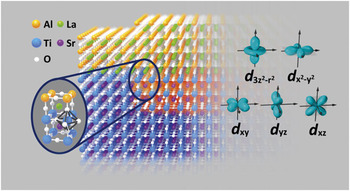
Artist’s impression of the LaAlO3/SrTiO3 interface. In the left part of the structure, a three-unit cell LaAlO3 layer is covering the Ti-terminated SrTiO3 substrate, yielding an insulating interface. On the right side, the LaAlO3 layer thickness is four unit cells, which leads to a conducting interface (as indicated by the red coloring of the SrTiO3 top layers). The different Ti-3d orbitals are shown to the right. The t 2g orbitals d xy, d yz, and d xz are involved in the electronic/magnetic properties. The d 3z2–r2 and d x2–y2 e g orbitals are at higher energy, but are relevant for other oxide combinations involving the cuprates and nickelates. The zoom-in shows a magnification of the interface, with an oxygen octahedron surrounding an interface Ti atom. (Figure courtesy of X. Renshaw Wang, University of Twente.)

A special aspect of the oxide 2DEGs, which because of their electronic correlations and rich physics are also called two-dimensional electron liquids, Reference Breitschaft, Tinkl, Pavlenko, Paetel, Richter, Kirtley, Liao, Hammerl, Eyert, Kopp and Mannhart21 is the steepness of the confining potential. The ionic nature of these crystals, with their possibility for ferro- and para-electric responses to electric fields, as well as the polarizability of the oxygen atoms gives rise to very strong electric field screening. Typically, the interface 2DEG in the oxides extends only a few unit cells or nanometers into the abutting crystals. Reference Basletic, Maurice, Carretero, Herranz, Copie, Bibes, Jacquest, Bouzehouane, Fusil and Barthelemy22
Advanced materials tailoring and orbital engineering
Typical electron mobility values of about 100–2000 cm2/Vs are found at low temperatures for common LaAlO3/SrTiO3 interfaces, depending on the details of the fabrication. At room temperature, electron-phonon interactions set the mobility to about 7 cm Reference Cohen, Parks and Dekker2 /Vs. Reference Mannhart and Schlom23
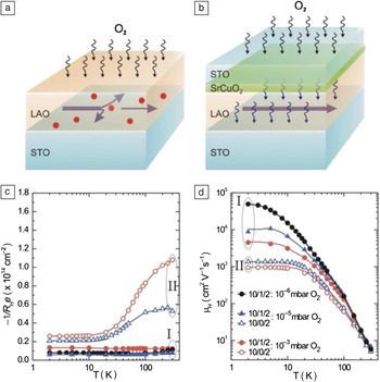
Using optimized procedures for the growth and annealing of samples, involving lower than usual growth temperatures (650°C instead of 800°C), low temperature mobility values of up to 6600 cm2/Vs were obtained. Reference Caviglia, Gariglio, Cancellieri, Sacépé, Fête, Reyren, Gabay, Morpurgo and Triscone24 By optimizing the surface of LaAlO3 using chemical and electronic techniques, mobilities exceeding 20,000 cm2/Vs were achieved, with concomitant reduction of the interface charge carrier density. Reference Xie, Bell, Hikita, Harashima and Hwang25 Recently, Huijben et al. showed that by incorporating a SrCuO2 capping layer on top of LaAlO3, the mobility could be greatly enhanced, up to 50,000 cm2/Vs at T = 4.2 K (see Figure 2 ). With this capping layer, a low and practically temperature-independent carrier density was found, which signals an efficient elimination of oxygen vacancies as charge donors and impurity potentials. Reference Huijben, Koster, Kruize, Wenderich, Verbeeck, Bals, Slooten, Shi, Molegraaf, Kleibeuker, van Aert, Goedkoop, Brinkman, Blank, Golden, van Tendeloo, Hilgenkamp and Rijnders26
Effects of enhanced oxygen-intake by (a–b) capping the LaAlO3/SrTiO3 heterostructures with a 1 unit cell SrCuO2 + 2 unit cells SrTiO3 coverage. (c) The temperature dependence of the carrier density, for uncapped (open symbols) and capped systems (closed symbols), showing the elimination of a thermally activated contribution to the carrier density, attributed to oxygen vacancies. (d) The concomitant increase in the mobility. Reprinted with permission from Reference 26. ©2013 Wiley.

At these high mobilities, Shubnikov-de Haas quantum oscillations in the resistance at high magnetic fields are resolved, Reference McCollam, Wenderich, Kruize, Guduru, Molegraaf, Huijben, Koster, Blank, Rijnders, Brinkman, Hilgenkamp, Zeitler and Maan27 but interestingly, so far no clear-cut quantum Hall effect has been reported for such interfaces. The reason for this is not yet clear, but it may be related to the multiband/multiorbital nature of the conductivity.
To further elucidate this multiband/multiorbital character, Reference Tokura and Nagaosa28 we again consider bulk crystalline SrTiO3. In this insulating compound, the Ti4+ ions are in a 3d 0 electron configuration, and when doped with electrons, the conduction band formed by its 3d orbitals is partially filled. The crystal field splits the 3d manifold into the lower lying t 2g levels (d xy, d xz, and d yz) and the e g levels (d x2–y2 and d 3z2–r2 ), which are about 3 eV further up in energy. These different orbital states are depicted in Figure 1. At the interface, additional level splitting occurs due to the symmetry breaking and to possible deformations and rotations of the oxygen octahedra surrounding the Ti. The d xy orbitals, oriented parallel to the interface, form the lowest lying band and have the lowest effective mass. Reference Salluzzo, Cezar, Brookes, Bisogni, De Luca, Richter, Thiel, Mannhart, Huijben, Brinkman, Rijnders and Ghiringhelli29 The heavier, more anisotropic d xz and d yz states have their band edge only slightly (in the 10 meV range) above that of the d xy band, and thus also become easily populated. The 2D-confinement furthermore leads to a discretization of the electron momenta in the direction perpendicular to the interface.
Finally, the carrier density as well as the d xy/d yz,d xz level splitting vary as a function of depth from the interface, and with this the orbital character of the mobile electrons also varies. Reference Mannhart and Schlom23,Reference Delugas, Filipetti, Fiorentini, Bilc, Fontaine and Ghosez30 The result is a complex, carrier density-dependent multiband/multiorbital system, in which the different bands are expected to exhibit different properties in terms of mobility and magnetic character. For the samples in Figure 2, up to five different high mobility bands have been seen in Shubnikov-de Haas oscillations, with varying effective masses in the 0.9–3 me range. Reference McCollam, Wenderich, Kruize, Guduru, Molegraaf, Huijben, Koster, Blank, Rijnders, Brinkman, Hilgenkamp, Zeitler and Maan27
While a complicating factor, the special orbital aspects of the complex oxide 2DEGs also allow for a new paradigm for materials tailoring: “interface orbital engineering.” This has been introduced on theoretical grounds by Hansmann et al., who suggested that the orbital state of high-T c superconductors, with its characteristic partially filled 3d x2–y2 -like band, can be mimicked by the LaNiO3-LaAlO3 interface. Reference Hansmann, Yang, Toschi, Khaliulin, Andersen and Held31 In its bulk metallic state, LaNiO3 has one electron per unit cell in the two-fold degenerate e g-orbital states. When sandwiched between LaAlO3, the d 3z2–r2 levels are shifted to higher energy, and the partially filled d x2–y2 band is predicted to form the only conduction band, a situation similar to the cuprates. X-ray reflectivity studies indeed show a shift in orbital occupation, Reference Benckiser, Haverkort, Brück, Goering, Macke, Frañó, Yang, Andersen, Cristiani, Habermeier, Boris, Zegkinoglou, Wochner, Kim, Hinkov and Keimer32,Reference Boris, Matiks, Benckiser, Frañó, Popovich, Hinkov, Wochner, Castro-Colin, Detemple, Malik, Bernhard, Prokscha, Suter, Salman, Morenzoni, Cristiani, Habermeier and Keimer33 although smaller than predicted, and a Mott insulator state is observed by DC transport measurements in ultrathin LaNiO3/LaAlO3 superlattices. Reference Liu, Okamoto, van Veenendaal, Kareev, Gray, Ryan, Freeland and Chakhalian34 So far, high-T c superconductivity has not been observed, but the concept of orbital engineering at interfaces is still in its infancy and may hold surprises for the future.
It is also noteworthy that hole-doped conductivity has been realized in LaVO3 when sandwiched between LaAlO3. Reference Higuchi, Hotta, Susaki, Fujimori and Hwang35 Together with n-doped interfaces such as LaAlO3/SrTiO3 these two-dimensional hole gases (2DHG) provide an interesting basis for novel devices, such as p–n junctions and closely coupled 2DEG/2DHG systems. The latter are of interest for thermoelectrics and for the exploration of exciton Bose–Einstein condensation in correlated electron systems. Reference Rademaker, van den Brink, Hilgenkamp and Zaanen36
Superconductivity and magnetism
The rich phenomenology of the complex oxide interfaces becomes especially apparent from the fact that under certain conditions, superconductivity Reference Reyren, Thiel, Caviglia, Fitting Kourkoutis, Hammerl, Richter, Schneider, Kopp, Rüetschi, Jaccard, Gabay, Muller, Triscone and Mannhart37 as well as magnetic effects Reference Brinkman, Huijben, van Zalk, Huijben, Zeitler, Maan, van der Wiel, Rijnders, Blank and Hilgenkamp38 are observed. For LaAlO3/SrTiO3 interfaces, superconductivity occurs below about 300 mK, which is similar to values found in bulk electron-doped SrTiO3. It has been verified that this superconducting phase has a true 2D character though, and electric field effect experiments, using voltages applied to a metallic gate-electrode on the backside of the substrate, have mapped out the dependence of the critical temperature on the carrier concentration. Reference Caviglia, Gariglio, Reyren, Jaccard, Schneider, Gabay, Thiel, Hammerl, Mannhart and Triscone39
An outstanding question is whether the observed superconductivity has additional special features, such as an unconventional order parameter symmetry or unusual finite momenta of the Cooper pairs, Reference Michaeli, Potter and Lee40 the electron pairs that establish the superconducting state. Also, the multiorbital character of the conductance at the interfaces is again of interest here: do the d xy and the d xz, d yz electrons both contribute to the superconductivity? Are the Cooper pairs arising from predominant interband or intraband pairing, Reference Fernandes, Haraldson, Wölfle and Balatsky41 and is there a special role for the transition from single- to multiband occupation with increased carrier density? Reference Joshua, Pecker, Ruhman, Altman and Ilani42
Such questions become particularly tantalizing when considering the reported coexistence of superconductivity and magnetism. Magnetic effects were initially observed in the form of strong magnetoresistance and temperature dependence of the resistance that is characteristic for Kondo scattering, in which a cloud of mobile electrons surrounds localized magnetic moments. Reference Brinkman, Huijben, van Zalk, Huijben, Zeitler, Maan, van der Wiel, Rijnders, Blank and Hilgenkamp38 Later studies have shown the coexistence of different ferromagnetic, dia-, and paramagnetic phases. Reference Ariando, Wang, Baskaran, Liu, Huijben, Yi, Annadi, Barman, Rusydi, Dhar, Feng, Ding, Hilgenkamp and Venkatesan43 These magnetic effects are found, in particular, for LaAlO3/SrTiO3 interfaces grown by pulsed laser deposition at comparatively high oxygen pressures (>10–3 mbar), in which a different ground state appears at the superconducting interfaces, which are typically grown at around 10–4 mbar.
Also the thickness of the LaAlO3 film plays a role; magnetic effects are more prominently observed for LaAlO3 film thicknesses exceeding about 10 unit cells. In several subsequent studies, magnetic effects and superconductivity have been reported to occur on the same sample. Reference Dikin, Mehta, Bark, Folkman, Eom and Chandrasekhar44–Reference Li, Richter, Mannhart and Ashoori46 While investigations are still ongoing to prove whether this coexistence is truly an intrinsic effect or whether this is due to sample inhomogeneity or phase separation effects, an interesting scenario emerges that superconductivity could be carried by one type of the carrier, for example the heavier d xz and d yz electrons, Reference Nakamura and Yanase47 whereas the magnetism is provided by the d xy electrons, possibly mediated by interactions with localized magnetic moments. Reference Salluzzo, Gariglio, Stornaiuolo, Sessi, Rusponi, Piamonteze, De Luca, Minola, Marré, Gadaleta, Brune, Nolting, Brookes and Ghiringhelli48 Also other suggestions have been made, for example, that the magnetism arises in the d xz and d yz bands related to their anisotropic nature. Reference Chen and Balents49 Obviously, a complete understanding on the mechanisms for the interface superconductivity and magnetism, and their interplay, is still in development.
Nanostructures and transistors
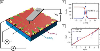
The sharp phase transitions in the complex oxide 2DEGs, such as the insulator-to-metal transition between 3–4 unit cells in the case of LaAlO3/SrTiO3, Reference Thiel, Hammerl, Schmehl, Schneider and Mannhart10 provide a tantalizing basis for applications in future nanoscale electronic circuitry. Levy and co-workers from the University of Pittsburgh have provided an alluring demonstration for this in a series of experiments Reference Cen, Thiel, Hammerl, Schneider, Andersen, Hellberg, Mannhart and Levy50–Reference Ma, Huang, Ryu, Bark, Eom, Irvin and Levy52 (see Figure 3 ). Starting with insulating samples of three unit cells of LaAlO3 on SrTiO3, they induced conductivity in the LaAlO3/SrTiO3 interface underneath the voltage-biased tip of a conducting atomic force microscopy, traversing over the LaAlO3 surface. This way, (super-)conducting lines only a few nanometers wide were written and subsequently erased, and small devices such as side-gated field-effect transistors were realized. The understanding at this moment is that the tip voltage bias leads to selective removal of OH– groups at the LaAlO3 surface, occurring as a result of ionization of water at this surface, leaving behind excess positive charges in the form of H+-ions. Reference Bi, Bogorin, Cen, Bark, Park, Eom and Levy53 These positive ions provide a local field-effect gating, enough to drive the insulator-to-metal transition. While this “water cycle” is not directly suited for widespread technology, these experiments beautifully demonstrate the possibility of realizing nanoscale electronic device structures and the sharpness of the potential profiles that can be created in these oxides.
(a) Schematic of the atomic force microscopy (AFM) nanowriting technique, in which a conducting path is formed in an insulating matrix of three unit cells of LaAlO3 on SrTiO3 by the action of a voltage-biased AFM tip. (b) By reversing the polarity of the AFM tip, the conducting line can be cut; the concomitant reduction of the conductance reveals the line width of the conducting path, in this case having a full width at half-maximum (FWHM) value of 8 nm. (c) With this writing method, superconducting nanowires also have been realized. (Figure courtesy of P. Irvin and J. Levy, University of Pittsburgh.)

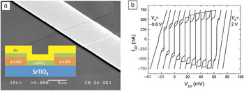
The development of field-effect transistors with metallic gates is also advancing rapidly. Initial studies have been performed using gates at the backsides of the SrTiO3 substrates, showing the possibility of switching superconductivity on and off. Reference Caviglia, Gariglio, Reyren, Jaccard, Schneider, Gabay, Thiel, Hammerl, Mannhart and Triscone39 More recently, metal oxide interface field-effect transistors (MOIFETs) have also been demonstrated in top-gated geometries, Reference Förg, Richter and Mannhart55–Reference Eerkes, van der Wiel and Hilgenkamp58 enabling local modulation of the (super-)conductivity with modest gate voltages (see Figure 4 ). A range of experiments is now within reach, reminiscent of the quantum/nano research done on GaAs/AlGaAs, such as single-electron manipulation, with the additional attraction of the rich physics of the oxides—displayed, for example, in its superconductivity—and the versatility in materials combinations.
Modulation of superconductivity by top-gating in LaAlO3/SrTiO3 two-dimensional electron gases (2DEGs). (a) Scanning electron microscopy image of a top-gated 2DEG structure in a crossbar geometry. The inset shows the definition of the 2DEG structure, using amorphous LaAlO3 as an insulator. Reference Schneider, Thiel, Hammerl, Richter and Mannhart54 (b) Superconducting field-effect transistor action; the critical current of the 2DEG is modulated by a voltage applied to the top gate. Reference Eerkes, van der Wiel and Hilgenkamp58

Tunable spin-orbit coupling and topological insulators
Another special feature of the complex oxide 2DEGs is the large and tunable Rashba spin-orbit coupling, which is of great interest for spintronics. Rashba spin-orbit coupling arises when an electron experiences an electric field perpendicular to its direction of motion, which in the case of the oxide 2DEGs implies a field perpendicular to the interface. Reference Caviglia, Gabay, Gariglio, Reyren, Cancellieri and Triscone59,Reference Ben Shalom, Sachs, Rakhmilevitch, Palevski and Dagan60 The structural inversion symmetry breaking at the interface already provides a strong field and concomitant spin-orbit coupling, which can be further enhanced and manipulated by applying external gate voltages. One of the prospects arising from this is the realization of a functional spin field-effect transistor, Reference Datta and Das61 in which spin-precession is controlled by an external gate. In this, the combination of top- and backgating may be particularly powerful.
Finally, oxide interfaces may also play a role in the rapidly developing field of topological insulators. Predictions for 3D-topological insulator behavior in iridium-based pyrochlores such as Y2Ir2O7 Reference Pesin and Balents62,Reference Yang and Kim63 and the bismuthate perovskite YBiO3 Reference Jin, Rhim, Im and Freeman64 have been made, which are awaiting experimental confirmation. Particularly fruitful in this respect will be the large bandgap and bulk resistivity of the oxides. When these predictions will be confirmed experimentally, the complex oxides will prove themselves all the more as true gemstones of physics.
Conclusion
In addition to the many special bulk properties of complex oxides, their interfaces present exciting additional platforms for the creation of novel electronic and magnetic phases. With enhanced control at the materials science of these oxides, for example with respect to substrate preparation and thin-film growth, new materials combinations can now be realized with atomic precision. It is to be expected that further discoveries will arise from such interfaces, of which higher temperature superconductivity would be a most tantalizing prospect. Because of their versatility and stability, the fact that they can be fabricated using relatively conventional thin-film growth techniques, and the possibility to controllably create field-effect transistors and functional nanostructures, complex oxides and their interfaces present serious candidate materials systems for future nano-electronic device technologies.
Acknowledgments
H.H. would like to credit J. Levy and J. Mannhart for their valuable contributions and thank X. Renshaw Wang for his help with Figure 1.