Introduction
With the introduction of new 5G frequency bands, such as the recently authorized 5G N78 (3.4–3.6 GHz) and N79 (4.8–5 GHz) bands, the number of antennas within 5G terminals has to be further increased. However, the internal space of terminal devices is already filled with various functional components, and the available room for new antennas is therefore becoming very limited [Reference Chen, Li and Lee1–Reference Jayant, Srivastava and Kumar4]. The above background suggests an urgent demand for those antennas with specific characteristics such as dual target band coverage, low profile, and very compact size. This type of antenna is not only of great research significance in the application of terminal antennas but also offers advantages in optimizing network capacity and frequency allocation [Reference Dai, Huang, Hu, Wu, Xing and Yu5].
Currently, various methods for designing dual-frequency patch antennas have been proposed, which can be generally categorized into two types. For the first type, a single radiating structure is used to achieve a dual-band coverage, either through exciting high-order modes [Reference Liu, Zhu, Liu, Zhang and Fu6–Reference Chang, Zhang and Wang10] or through introducing radiating slots into the antenna structure [Reference Boukarkar, Lin, Yu, Mei, Jiang and Yu11–Reference Lee, Yang and Kishk15]. In [Reference Liu, Zhu, Liu, Zhang and Fu6], three modes of a square patch are stimulated and controlled by loading shorting pins, enabling a dual-band operation. However, using more than two higher-order modes typically requires a large antenna footprint. In [Reference Boukarkar, Lin, Yu, Mei, Jiang and Yu11], U-shaped radiation slots are added to a single patch to generate the resonances in high bands, but this method usually requires a high profile for effective radiation of the slot.
The second approach incorporates multiple resonant structures, such as establishing multiple current paths [Reference Peng, Ruan and Wu16–Reference Zhang, Zhang, Pan and Duan18], stacked patches [Reference Yang, Fan and Liu19–Reference Liu, Wu and Fang23], and introducing parasitic structures [Reference Qian, Chen, Chu, Xue and Lancaster24–Reference Chang and Liu28]. In [Reference Wong, Chen and Li17], a coplanar strip feedline is employed to simultaneously excite two compactly arranged patches for dual-band coverage. In [Reference Liang, Liu, Li and Long22], a circular coupler is employed to feed a via-loaded ring on the bottom layer and a circular patch on the top layer, which achieve coverage in dual frequency bands. In [Reference Qian, Chen, Chu, Xue and Lancaster24], a similar microstrip patch antenna structure is parasitically introduced on the right side of a single-layer dual-frequency microstrip patch antenna through electric coupling, which achieves bandwidth expansion in two frequency bands. Generally, these designs can achieve wide bandwidths. However, multiple radiating structures are involved either in planar expansion form or in stacked form, which inevitably leading to a large footprint or a high profile.
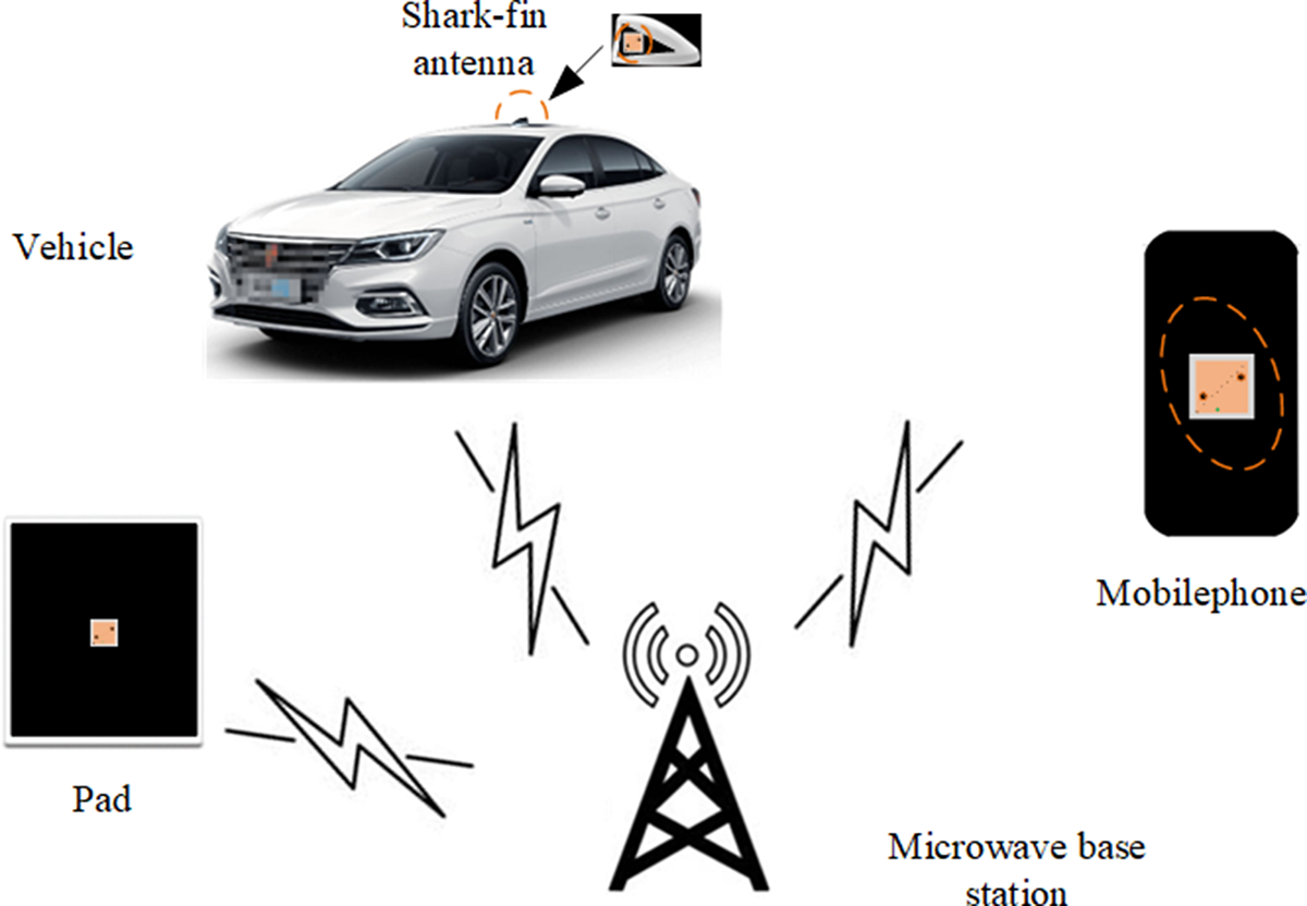
A dual-band quarter-mode substrate integrated waveguide (QMSIW) antenna with a further reduced footprint is introduced in this paper. The QMSIW not only inherits the advantage of multiple modes from SIW structure but also features a very compact size. In this design, two modes (TE110 and TE220) of a single QMSIW structure are used to achieve the dual-band operation. A capacitive-loading structure is then employed in the QMSIW to tune the high frequency mode, thereby flexibly adjusting the frequency ratio of the two bands. On this basis, the dual-band bandwidth can be enhanced by coupling with a parasitic QMSIW structure. Due to the frequency-tunable and miniaturized characteristics of the proposed antenna, as shown in Fig. 1, it can not only be applied to mobile devices but also be adapted to scenarios such as V2V communication [Reference Zhou, Wu, Wang, Sun, Liu, Mumtaz, Guizani and Niyato29].
Potential application scenario for the proposed antenna.

Antenna design
Two antenna designs based on the QMSIW structure are introduced in this section.
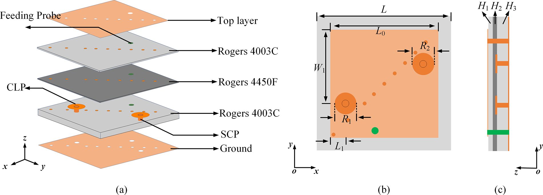
Figure 2(a) shows the configuration of Antenna I (magnetic coupling antenna). Figure 2(b) and (c) depicts the top and side views of the antenna. The square-shaped antenna consists of two QMSIW structures, which are the driven QMSIW on the lower right and the parasitic QMSIW on the upper left respectively. The two QMSIW structures achieve magnetic coupling through the shared shorting pins. The number of shorting pins can be changed to control the coupling strength. The antenna is constructed by three substrate layers, including two layers of Rogers 4003C (permittivity: 3.55, loss tangent: 0.0027) and one prepreg layer of Rogers 4450F (permittivity: 3.66, loss tangent: 0.004). To adjust the high frequency mode, a capacitive-loading structure is built on the lower Rogers 4003C substrate in each QMSIW structure, which is composed of a capacitive-loading patch (CLP) and a short circuit post (SCP). The CLP is connected to the ground plane through the SCP. A feeding probe within the driven QMSIW structure is used to properly excite the antenna.
Configuration of the proposed Ant. I (H 1 = 0.813, H 2 = 0.17, H 3 = 0.406, L = 50, L 0 = 20, L 1 = 2.9, W 1 = 14.2, R 1 = 4.8, R 2 = 4.9. Unit: mm).

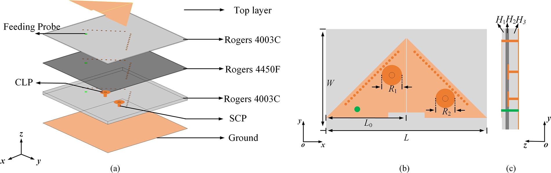
Figure 3 shows the configuration of Antenna II (electric coupling antenna). Figure 3(b) and (c) depicts the top and side views of the antenna. The two QMSIW structures are coupled to each other through the gap between them (electric coupling), forming a triangular-shaped antenna. The size of the gap can be changed to control the coupling strength. The frequency tuning mechanism of Ant. II is similar to that of Ant. I. It also can be excited by using a probe feeding.
Configuration of the proposed Ant. II (H 1 = 0.813, H 2 = 0.17, H 3 = 0.406, L = 50, W = 50, L 0 = 21, R 1 = 5.6, R 2 = 5.5. Unit: mm).

Analysis of a single QMSIW structure
The two modes of TE110 mode and TE220 mode are selected to achieve dual-band coverage in a single QMSIW structure. Due to their circular symmetric E-field distributions, these two modes can still be supported after the SIW structure is cut to form the QMSIW structure [Reference Althuwayb and Chaturvedi30, Reference Althuwayb31].
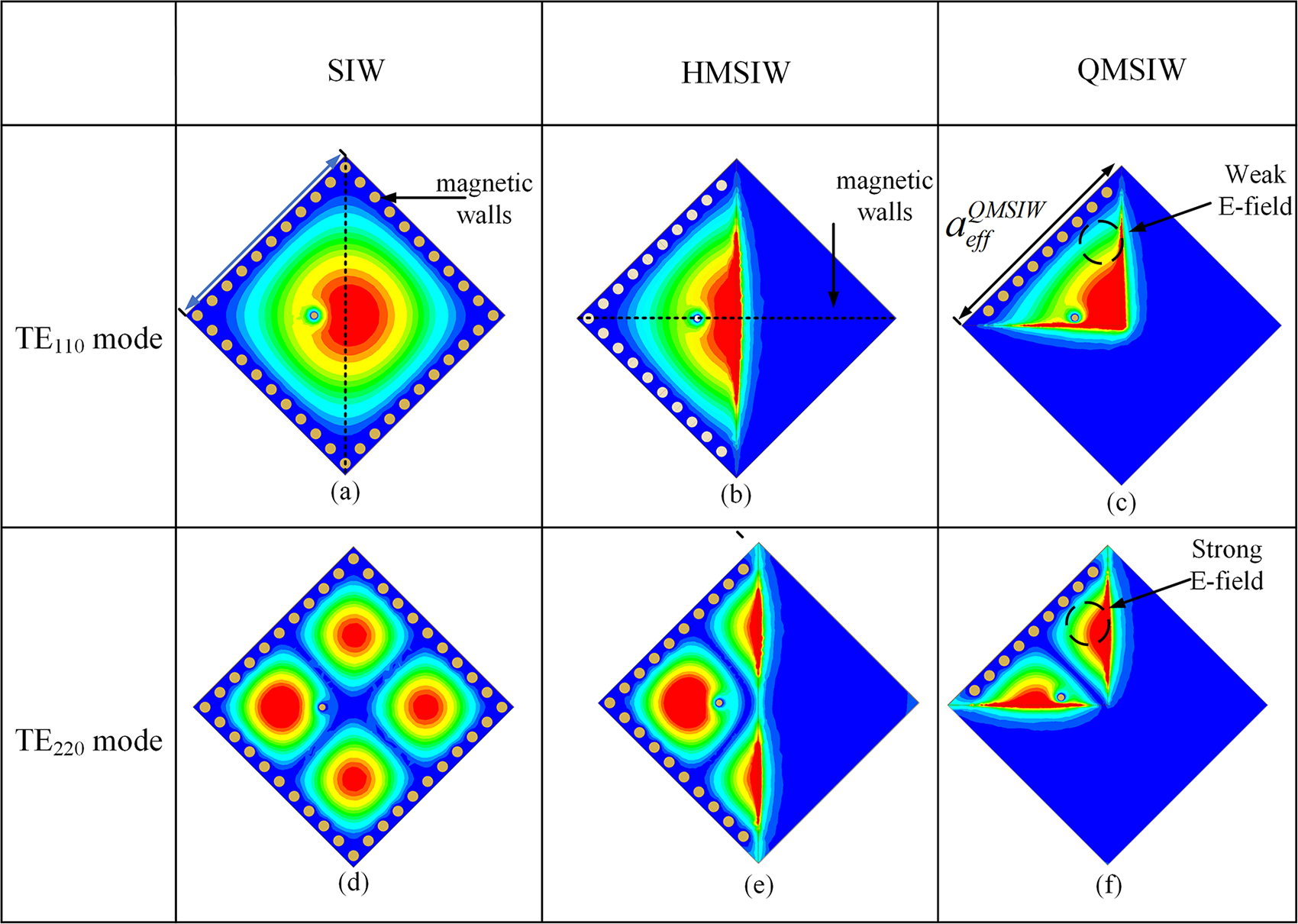
Figure 4 shows the evolution process of the proposed single QMSIW structure. It is learned that a complete SIW structure is firstly cut along the equivalent magnetic wall to form an HMSIW structure. Then the HMSIW structure is further cut along the equivalent magnetic wall to form the QMSIW structure. Compared to the traditional SIW cavity, the overall size of the QMSIW structure can be reduced by more than 3/4 while the two resonant modes keep almost unchanged.
E-field distribution of TE110 mode in (a) SIW, (b) HMSIW, (c) QMSIW, and E-field distribution of TE220 mode in (d) SIW, (e) HMSIW, and (f) QMSIW.

The initial side length of the QMSIW structure  $a_{eff}^{QMSIW}{\text{ }}$can be determined by setting the TE110 mode resonate at 3.5 GHz using the following equations:
 \begin{equation}f_{T{E_{mn0}}}^{QMSIW} = \frac{c}{{2\sqrt {{\mu _r}{\varepsilon _r}} }}\sqrt {{{\bigg(\frac{m}{{a_{eff}^{QMSIW}}}\bigg)}^2} + {{\bigg(\frac{n}{{a_{eff}^{QMSIW}}}\bigg)}^2}} \end{equation}
 \begin{equation}a_{eff}^{QMSIW} = a_{eff}^{SIW} + \Delta {\omega ^{QMSIW}}\end{equation}
where  $a_{eff}^{SIW}{\text{ }}$is the equivalent length of the initial SIW structure, and
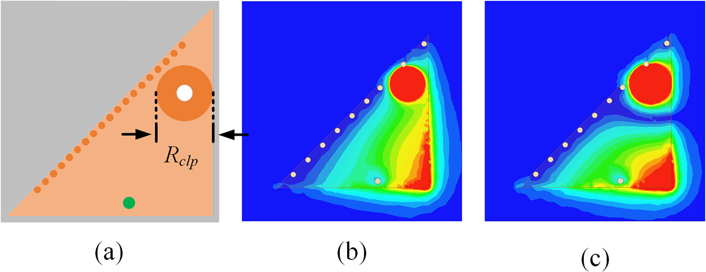
 $\Delta {\omega ^{QMSIW}}$is the additional length due to the edge field effect of the equivalent magnetic wall [Reference Chaturvedi, Kumar and Raghavan32]. With the initial calculations, the TE110 mode can operate at 3.5 GHz, but the corresponding TE220 mode resonates at 7.2 GHz, which does not meet the design requirements for covering the N79 4.9 GHz frequency band. To adjust the TE220 mode while not affect the TE110 mode, a capacitive loading structure can be introduced at a location where the TE110 mode has a weak E-field distribution and the TE220 mode has a strong E-field distribution, as shown in Fig. 4(c) and (f). It is expected that tuning the loading structure will have a significant impact on the TE220 mode without affecting the TE110 mode.
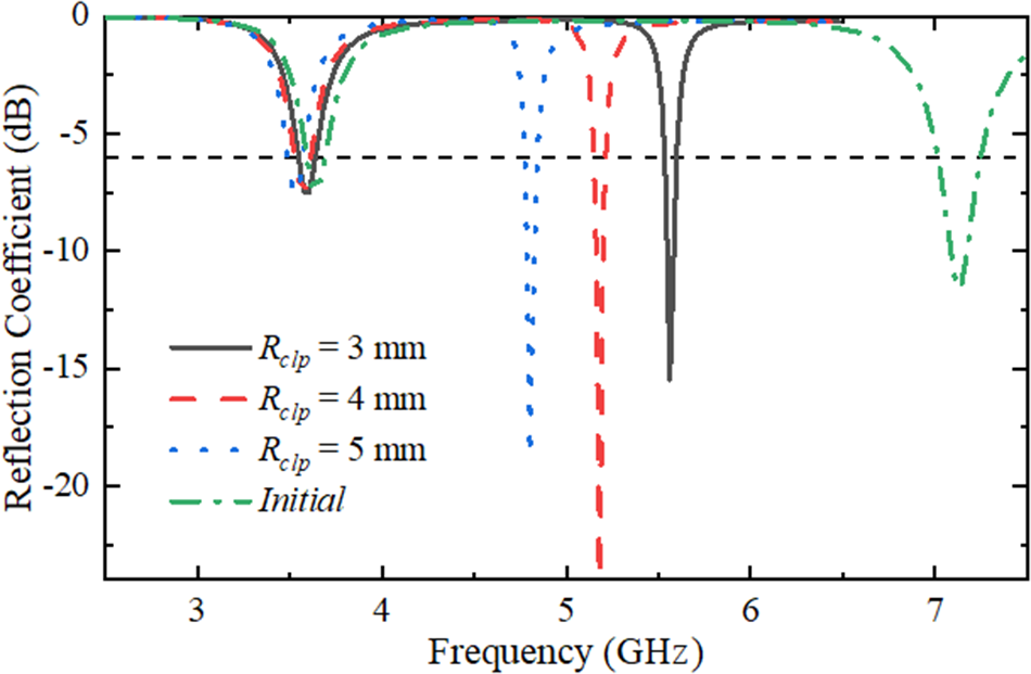
Figure 5 illustrates the QMSIW with capacitive loading structure and the corresponding E-field distributions of TE110 mode and TE220 mode. It can be observed that the introduction of CLP and SCP has almost no effect on the E-field distribution of the TE110 mode while it significantly affects the E-field distribution of the TE220 mode. The resonance of TE220 mode can be regarded as a parallel LC circuit, and the capacitive loading increases the equivalent capacitance, which causes its resonant frequency to shift to a lower frequency. Figure 6 shows the simulation results for validation, where we can find that with the increase of CLP radius (Rclp), the resonance frequency of TE220 mode moves quickly downward to 4.9 GHz band while the TE110 mode remains relatively stable.
(a) QMSIW structure with capacitive loading. (b) TE110 mode in the QMSIW structure. (c) TE220 mode in the QMSIW structure.

Reflection coefficients with different rclp.

Case of magnetic coupling
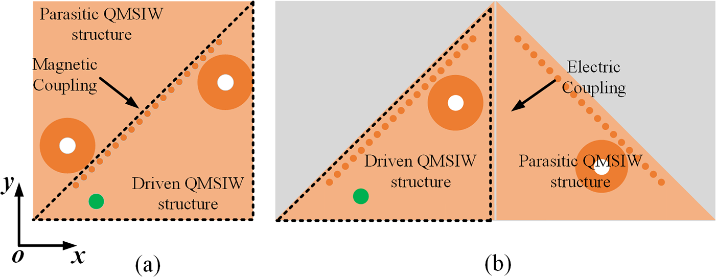
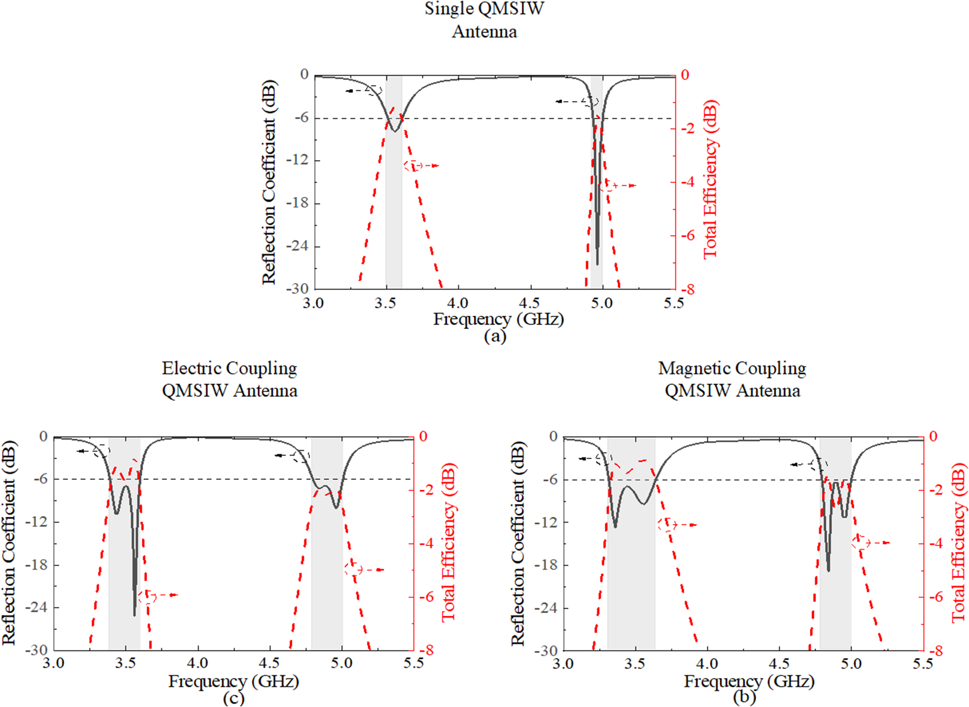
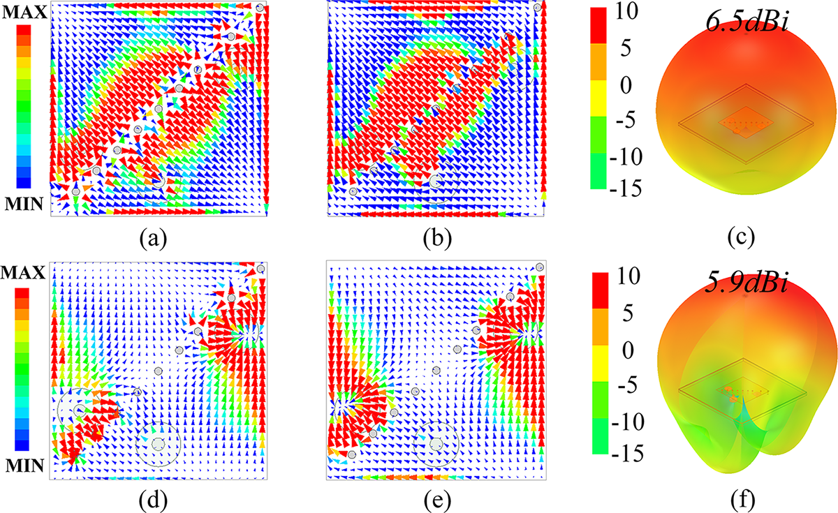
In this section, bandwidth expansion through magnetic coupling to a parasitic QMSIW structure is analyzed. The schematic diagram of the antenna structure is illustrated in Fig. 7(a). It can be found that a parasitic symmetrical QMSIW structure is coupled to the driven QMSIW antenna through shared shorting pins (magnetic coupling). For comparison, Fig. 8(a) firstly shows the simulated reflection coefficient and total efficiency of a single QMSIW antenna, where we can find that the antenna operates in 5G N78 and N79 bands with only one resonance in each frequency band. Figure 8(b) then shows the simulated results of the magnetic coupled antenna. It is learned that once the two identical QMSIW resonators are properly coupled, two resonances can be effectively generated in each frequency band, leading to a significant expansion of the bandwidth. From the perspective of the coupled resonant cavity, the two resonant modes in each band can be considered as even and odd modes, respectively. For instance, Fig. 9(a) and (b) shows the current distributions of the antenna at 3.35 GHz and 3.55 GHz respectively. It can be found that at 3.35 GHz, the phases of the currents on the top surface of the two QMSIW structures are the same, indicating it is an even TE110 mode and. While at 3.55 GHz, the current phases are opposite, demonstrating the odd TE110 mode. The two modes in the high frequency 4.9 GHz band follow the same rules, as shown in Fig. 9(d) and (e). As depicted in Fig. 9(c) and (f), the magnetic coupled QMSIW antenna achieves effective half-space coverage in both the N78 and N79 frequency bands with simulated gains of 6.5 dBi and 5.9 dBi respectively.
The structures of (a) magnetic coupling QMSIW antenna and (b) electric coupling QMSIW antenna.

Simulated reflection coefficients and total efficiencies: (a) single QMSIW structure, (b) magnetic coupling antenna, and (c) electric coupling antenna.

Current distribution at (a) 3.35 GHz and (b) 3.55 GHz. (c) 3D radiation pattern at 3.5 GHz. Current distribution at (d) 4.85 GHz and (e) 4.95 GHz. (f) 3D radiation pattern at 4.9 GHz.

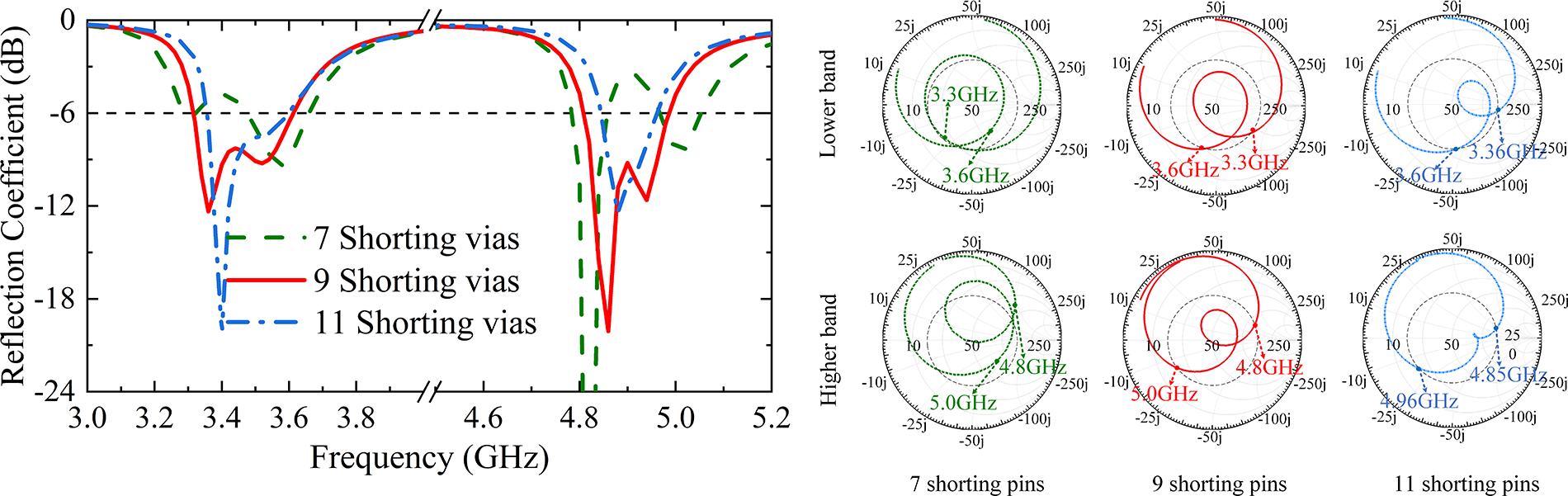
Subsequently, the number of shorting pins, which is a key factor influencing the strength of magnetic coupling, is analyzed. Figure 10 illustrates the reflection coefficients and corresponding Smith charts for the QMSIW antenna with 7, 9, and 11 shorting pins. It can be observed that as the number of shorting pins decreases, the coupling between the two resonant structures gradually strengthens. The two coupled modes become separated at each frequency band. Through optimization, the antenna with nine shorting pins has been selected as the most favorable one for achieving optimal bandwidth expansion.
The reflection coefficients and Smith circle diagrams of the QMSIW antenna with different shorting pins of 7, 9, and 11.

Case of electric coupling
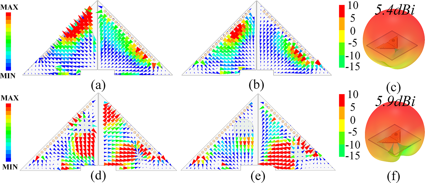
Previous study has confirmed that the utilization of parasitic structure through proper magnetic coupling can significantly enhance the bandwidth. In this section, the case of electric coupling is analyzed. Figure 7(b) shows the antenna structure. It can be found that a symmetrical parasitic QMSIW structure is coupled to the driven QMSIW antenna through the gap between the two structures. Figure 8(c) shows the simulated results of the electrically coupled antenna. Due to the proper coupling of the two QMSIW resonators, two resonances can be stimulated in each frequency band and the bandwidth are effectively enhanced. Figure 11(a)–(b) and (d)–(e) shows the current distributions of the antenna at low and high frequency band, respectively. It can be found that the two modes in each band can also be regarded as even and odd modes. Figure 11(c) and (f) gives the 3D radiation patterns, where we can find that the electrically coupled QMSIW antenna achieves good half-space coverage in both the N78 and N79 frequency bands as well, with simulated gains of 5.4 dBi and 5.9 dBi respectively.
Current distribution at (a) 3.45 GHz and (b) 3.55 GHz. (c) 3D radiation pattern at 3.5 GHz. Current distribution at (d) 4.85 GHz and (e) 4.95 GHz. (f) 3D radiation pattern at 4.9 GHz.

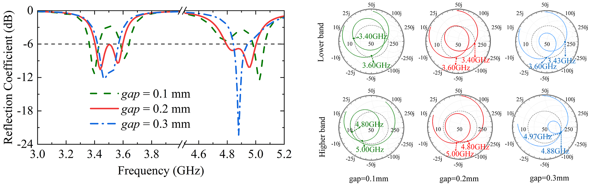
The key parameter of the coupling coefficient in electric coupling is discussed, that is the gap between the driven and parasitic resonators. Figure 12 shows the simulated results with different gap sizes of 0.1 mm, 0.2 mm, and 0.3 mm. It can be learned that as the gap size decreases, the coupling between the two resonant structures gradually strengthens. The antenna with a gap size of 0.2 mm achieves the optimized performance.
The reflection coefficient and Smith circle diagram of the antenna under different gaps in electrical coupling.

Results
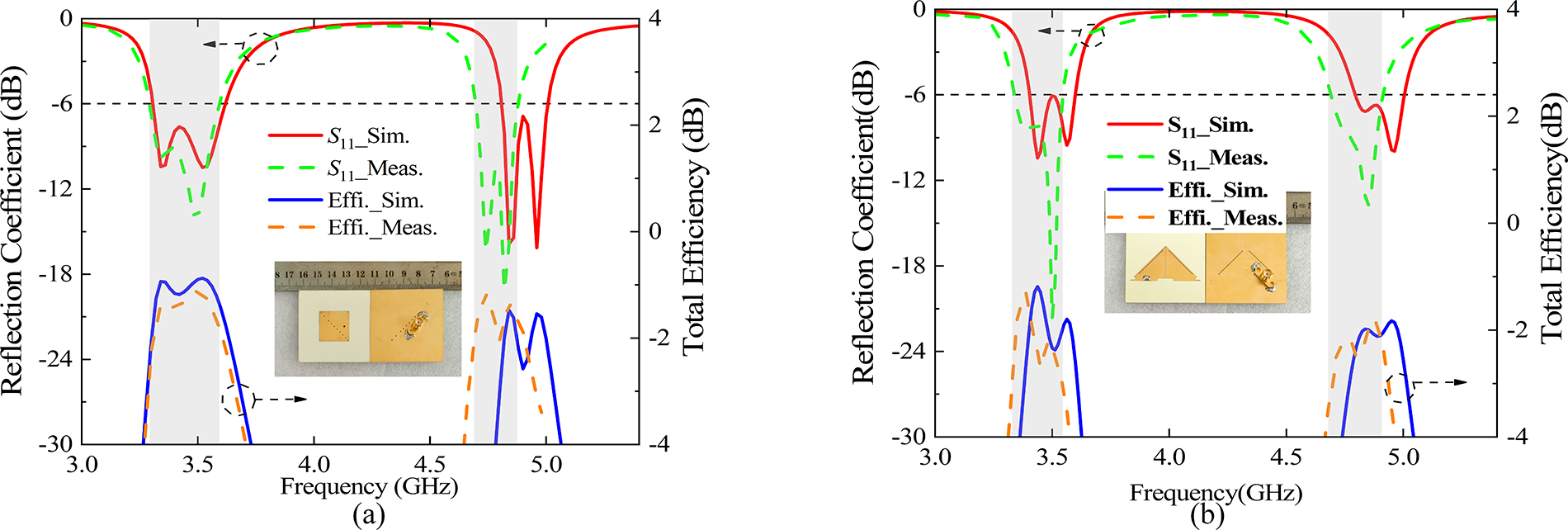
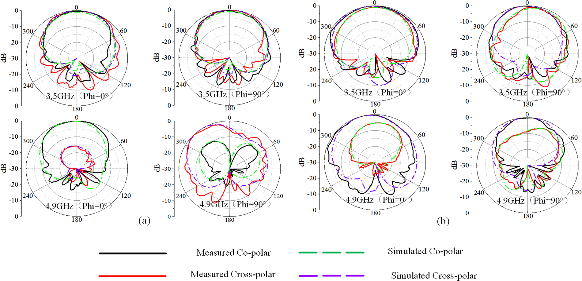
The proposed antennas are simulated using HFSS 2022, and the prototypes are fabricated and measured. Figure 13 shows the simulated and measured reflection coefficients and total efficiencies. The measurements validate the bandwidth enhancement of the two antennas. For Ant. I, a −6 dB impedance bandwidth of 8.72% (3.29–3.59 GHz) in the low-frequency band and 3.97% (4.69–4.88 GHz) in the high-frequency band is obtained. Clear dual resonances are observed in both frequency bands. The measured average total efficiency is about −1.52 dB (70.1%) in the lower frequency band and −1.62 dB (68.9%) in the higher frequency band. For Ant. II, the −6 dB impedance bandwidth is 6.73% (3.33–3.56 GHz) in the low-frequency band and 5% (4.68–4.92 GHz) in the high-frequency band. Dual resonances can also be found in both frequency bands. The measured average total efficiency is −2.23 dB (59.8%) in the lower frequency band and −2.26 dB (59.4%) in the higher frequency band. Figure 14 illustrates the simulated and measured radiation patterns. It can be seen that the proposed antenna achieves coverage of the upper half space.
Reflection coefficient and total efficiency of (a) Ant. I and (b) Ant. II.

Radiation patterns of (a) Ant. I and (b) Ant. II.

However, a deviation is observed in the measured results, particularly in the −6 dB impedance bandwidth. This discrepancy arises because the multilayer structure of the antenna is fabricated using pressure-assisted bonding, which causes the CLP to expand under compression. Consequently, the high-frequency bandwidth coverage is affected. During fabrication and testing, variations in temperature, mechanical stress, and other environmental factors can significantly impact antenna performance, leading to reduced robustness. This issue can be carefully considered and mitigated during simulation [Reference Zhang, Wu and Wei33].
Performance comparison
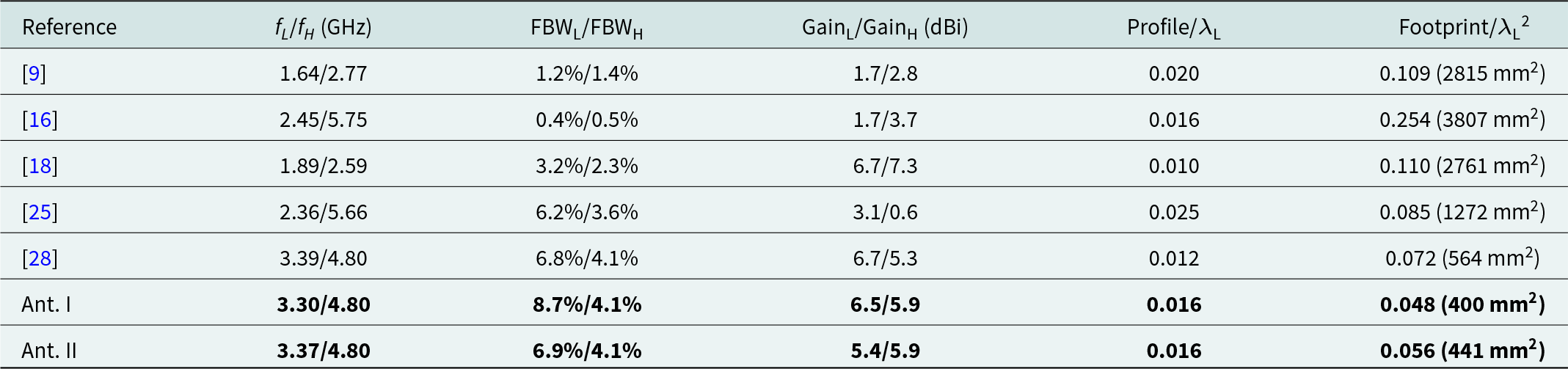
Table 1 presents a performance comparison between the proposed antenna and some typical dual-frequency antennas with low profiles of less than 0.02λ L, where λ L refers to the vacuum wavelength at the minimum frequency of the low frequency band. In some articles, there is a relatively large discrepancy between simulated and measured results. For the sake of ease in comparison, simulated results are utilized in the table. It can be observed that compared to the antennas in [Reference Yu, Gong, Wan and Chen9, Reference Peng, Ruan and Wu16, Reference Zhang, Zhang, Pan and Duan18] and [Reference Tak, Woo, Kwon and Choi25], the proposed antenna has a wider dual-band bandwidth and a smaller footprint. Compared to the antenna in [Reference Chang and Liu28], the proposed antenna has a comparable bandwidth but a smaller footprint.
Performance comparison of the dual-band antennas with low profiles of less than 0.02λ L

fL and fH refer to the lowest frequencies of the lower and higher bands, respectively.
Conclusion
In this paper, a kind of dual-band antenna is presented. The QMSIW structure with very compact size is employed in the design, achieving antenna miniaturization and enabling dual-band coverage through the utilization of TE110 mode and TE220 mode. Then, a capacitive-loading structure is introduced into the QMSIW to achieve flexible tuning of the resonant frequency of TE220 mode. On this basis, parasitic QMSIW structures are integrated to achieve bandwidth expansion, through magnetic and electric coupling respectively. The proposed two antennas are fabricated and measured, and the results indicate that they can offer dual-band coverage for N78 (3.4–3.6 GHz) and N79 (4.8–5 GHz) frequency bands with very compact footprints. The antennas have great potential for applications in 5G terminals.
Funding statement
This work was supported in part by the National Natural Science Foundation of China under Grant 62071256 and Grant 62371263, and in part by the Postgraduate Research and Practice Innovation Program of Jiangsu Province under Grant KYCX24_3653 and KYCX25_3723.
Xu Yang, Le Zhang, Xin Geng, Wen-Wen Yang, Wei Qin, and Jian-Xin Chen are with the School of Information Science and Technology, Nantong University, and also with the Nantong Research Institute for Advanced Communication Technologies, Chongchuan District, Nantong, 226019, China (e-mail: wwyang2008@hotmail.com).
Competing interests
The authors report no conflict of interest.

Le Zhang was born in Huaian, Jiangsu Province, China, in 2000. He received the B. Eng. degree from Nantong University, Nantong, in 2018. He is currently pursuing the M.S. degree in electromagnetic field and microwave technology in Nantong University, Nantong, China. His current research interest is microwave antenna.

Miao-Peng Shen was born in Nantong, Jiangsu Province, China, in 2000. He received the B.S. degree from Nantong University, Nantong, in 2022. He is currently pursuing the M.S. degree in electromagnetic field and microwave technology in Nantong University, Nantong, China. His current research interest is microwave antenna.

Xin Geng was born in Nantong, Jiangsu, China, in 1997. She received the B.S. degree from Jiangsu Ocean University, Lianyungang, China, in 2020, and the M.S. degree from Nantong University, Nantong, China, in 2023. She is currently pursuing the Ph.D. degree in electromagnetic field and microwave technology with Nantong University, Nantong, China.
Her current research interest focuses on microwave and millimeter-wave antenna theory and design.

Wen-Wen Yang received the B. Eng. degree in information engineering, M. Eng. degree and the Ph.D. degree in electrical engineering from the Southeast University (SEU), Nanjing, China, in 2007, 2010, and 2015, respectively.
Since 2015, He has been with the school of Electronics and Information at Nantong University, Nantong, China, where he is currently a professor. From August 2018 to August 2019, he was a visiting researcher with the Polytechnique Montréal, Montreal, Canada. His research interests include RF, microwave and millimeter-wave passive devices, active antenna array, and antennas for wireless communication. He serves as a reviewer for several IEEE and IET journals.

Jian-Xin Chen was born in Nantong, Jiangsu Province, China, in 1979. He received the B.S. degree from Huai Yin Teachers College, Jiangsu Province, China, in 2001, the M.S. degree from the University of Electronic Science and Technology of China (UESTC), Chengdu, China, in 2004, and the Ph.D. degree from the City University of Hong Kong, Kowloon, Hong Kong, in 2008. Since 2009, he has been with Nantong University, Jiangsu Province, China, where he is currently a professor. He has authored or coauthored more than 100 internationally referred journal and conference papers. He holds 25 Chinese patents and 3 U.S. patents. His research interests include microwave active/passive circuits and antennas, LTCC-based microwave and millimeter-wave filters and devices, and dielectric resonator (DR) filters and antennas.
Dr. Chen was a recipient of the “New Century Excellent Talents in University” of the Ministry of Education for China in 2011. He was the supervisor of several conference best paper award winners.

Xu Yang was born in Suqian, Jiangsu Province, China, in 2000. He received the B.S. degree from Nantong University, Nantong, in 2022. He is currently pursuing the M.S. degree in electromagnetic field and microwave technology in Nantong University, Nantong, China. His research interest is dual-band antennas for 5G terminal applications.