Introduction
Patterson is a pioneer in revealing the hazards of Pb to the environment and human being. Since then, remarkable progresses have been achieved in developing Sn-based solders.[Reference Abtew and Selvaduray1–Reference Kinyanjui, Lehman, Zavalij and Cotts3] SnAgCu is regarded as one of the most promising solders in electronic industry due to its good wettability and mechanical properties.[Reference Anderson, Cook, Harringa and Terpstra4–Reference Zhang, Yuan, Zhao, Zang and Li6] However, bulk Ag3Sn and Cu6Sn5 intermetallic compounds (IMCs) are easy to form in soldering. These brittle IMCs can isolate the matrix and work as the crack initiations, deteriorating the mechanical properties.[Reference Henderson, Gosselin and Sarkhel7] Consequently, it is necessary to suppress the formation of bulk IMCs to acquire better properties and reliability. It has been demonstrated that the size and morphology of the IMCs are significantly affected by cooling rates, and rapid quenching is thus commonly employed to optimize the solidification structure of solder point,[Reference Chuang, Tsao, Chung and Chang8] which is easily realized in laser soldering. However, rapid cooling is restricted in some practical cases, such as reflow soldering whose cooling rate is only several Kelvin per second.[Reference Lin, Srivatsan, Wang and Kovacevic9, Reference Dudek, Hunter, Kranz, Williams, Lau and Chawla10] To solve this problem, solders with low Ag content have been alternatively developed, yielding less possibility to form bulk IMCs. Moreover, less Ag reduces the cost concerns in commercial production. Among these solders, Sn0.3Ag0.7Cu (wt.%) is preferred because of its suppression on the formation of IMCs.[Reference Sundelin, Nurmi, Lepistö and Ristolainen11] In addition to the refined IMCs, solder droplets with highly spherical shape and, simultaneously, with narrow size distribution are intensively demanded in electronic industry such as ball grid array and flip chip.[Reference Minagawa, Kakisawa, Osawa, Takamori and Halada12] Solder droplets with uniform size guarantee the coplanarity of the package, which can reduce the possibility of opens of the connection. Moreover, a spherical solder droplet without satellite particles is beneficial to improve the reliability and yield strength. Although many methods such as electrical explosions, atomization, chemical reduction have been developed to produce solder droplets,[Reference Kwon, An, Ilyin and Tikhonov13–Reference Yagi, Ichitsubo, Matsubara, Yamaguchi, Kimura and Sasamori15] the highly spherical mono-sized SnAgCu droplets are still absent.
In this study, pulsated orifice ejection method (POEM) is applied to produce mono-sized Sn0.3Ag0.7Cu solder droplets with powder diameter ranging from 70.6 to 334.0 µm. Apart from the narrower size distribution, the droplet surface is smooth without any satellite particles. Further, both the composition and internal microstructure are highly homogenous throughout in the whole droplet. There are not any bulk Ag3Sn and Cu6Sn5 IMCs detected in the droplet, implying good mechanical properties of Sn0.3Ag0.7Cu solder.[Reference Sundelin, Nurmi, Lepistö and Ristolainen11] It is discussed that the POEM may also provide a promising method to prepare powders for three-dimensional (3D) printing.
Materials and methods
Pure Sn (99.95%), Ag (99.99%), and Cu (99.95%) are used to prepare commercial solder wires (1.0 mm in diameter) with nominal composition of Sn0.3Ag0.7Cu (wt.%) supplied by Hongjia Solder Manufacturing Co., Ltd., Kunshan, China. The preparation of droplets by POEM has been illustrated in Ref. Reference Miura, Dong, Fukue, Yodoshi, Takagi and Kawasaki16. For SnAgCu, the crucible was heated to the nominal temperature of 220 °C to get full liquid phase. After that, the rod in the ejection device moved up and down with a displacement of 7 µm to eject the droplets from the orifice at the bottom of the crucible. Then the falling droplets rapidly solidified at the atmosphere of highly pure Ar (99.999%) with 1 atm pressure. In this case, the diameter of the orifice ranges from 100 to 400 µm to prepare droplets with diameter from 70.6 to 334.0 µm. The composition of the solder wires and droplets were comparatively checked by chemical analysis. A scanning electron microscopy (SEM, JSM-6700F, JEOL) was used to examine the droplet morphology, while droplet structure was examined by x-ray diffraction (XRD, D/Max-2200, Rigaku) with Cu Kα radiation (λ = 0.154056 nm) at a scanning rate of 4 °/min. In the XRD measurement, one layer of SnAgCu droplets was closely dispersed onto an adhesive tape that was stuck on a piece of glass, and then characterized by the XRD. Some SnAgCu droplets were mounted with epoxy resin, which was followed by coarse grinding with diamond paper and fine polishing with Al2O3 abrasive paste. After that, the sample was etched by 5 vol.% HCl at room temperature for 22 s, and then coated with Pt. The internal structure and composition of droplets were characterized using optical microscopy (OM, Imager A2m, Carl Zeiss) and SEM equipped with energy-dispersive spectroscopy (EDS, INCA). HCl solution can extrude the grain boundaries and precipitations because of the different electric potentials in these phases. But etching time longer than 22 s should be avoided because residual etchant in the gap between droplet and epoxy resin can oxidize the edge of the droplet. Nitric acid was not used here due to its strong oxidization on the droplet: before observing the solidification structure, the droplet turns to be dark, possibly hindering further characterization. Backscattered electron images were also obtained by desktop SEM (Phenom ProX) equipped with EDS (AMPTEK).
Results and discussion
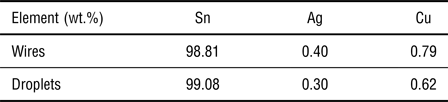
The chemical composition of the commercial solder wires and droplets are listed in Table I. As noted, the composition is close to the nominal one in spite of the negligible variation. In addition, there is negligible composition difference between solder wires and subsequent droplets, implying the absence of an obvious composition segregation during the POEM process.
Chemical composition of the solder wires and droplets.

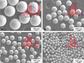
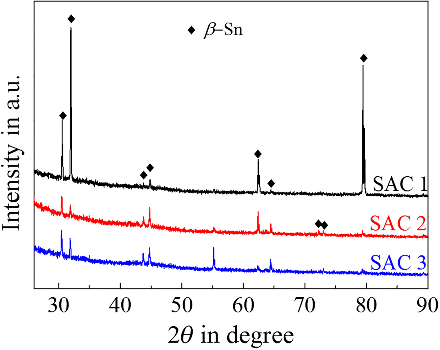
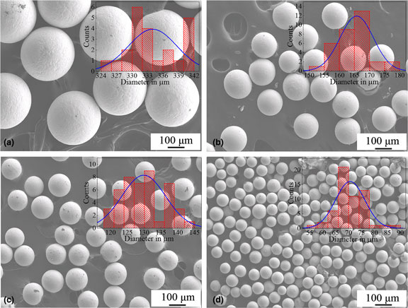
With different mechanical pressure and orifice size of POEM instrument, droplets with different diameters were prepared. Figure 1 shows the secondary electron images of the Sn0.3Ag0.7Cu droplets with various sizes. The figures also exhibit that most of the droplets are spherical, and the surface of the droplets is smooth without any satellite particles. Insets in Fig. 1 also indicate that the size of the droplets prepared is narrowly distributed around the average value. These droplet characteristics meet the requirements as electronic joint material especially for the laser soldering and electronic package.[Reference Chang, Hong and Pak17, Reference Kim, Jung, Lee, Jeong and Kang18] The XRD patterns of droplets with different size are displayed in Fig. 2. The peaks corresponding β-Sn (ICDD-JCPD S65-0296) is clearly identified. However, the peaks of IMCs are not detected by the XRD mainly due to the low content of Ag and Cu in these droplets. Further examinations are needed to certify the successful preparation of SnAgCu droplets.
SEM images showing the droplets morphology. The average diameters with deviation by normal distribution are (a) 334.0 ± 4.7 µm, (b) 165.8 ± 5.5 µm, (c) 129.8 ± 6.5 µm, and (d) 70.6 ± 5.7 µm. 23, 37, 46, and 59 droplets are counted in each case.

XRD patterns of SnAgCu droplets with diameter 334.0 µm (SAC 1), 165.8 µm (SAC 2), and 129.8 µm (SAC 3). All the peaks correspond to the β-Sn, while intermetallic compounds are not detected due to the low content of Ag and Cu.

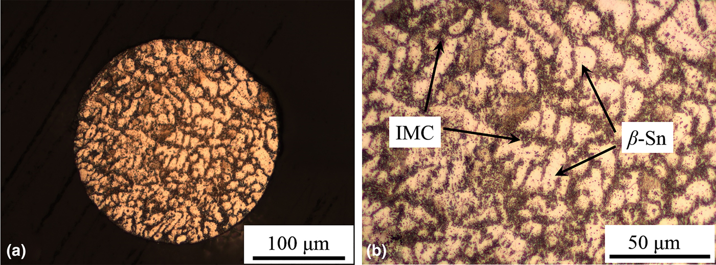
In addition to the mono-sized droplets, the cooling rate in POEM is very large enough to obtain amorphous structure.[Reference Miura, Dong, Fukue, Yodoshi, Takagi and Kawasaki16] Although this case cannot be realized in SnAgCu alloy, a well-refined solidification structure is possible to acquire. Figure 3 exposes the internal structure of a droplet of 334.0 µm. As expected, refined structure is uniformly distributed in the whole sample attributing to the high cooling rate. According to the SnAgCu phase diagram[Reference Kattner19] and previous studies,[Reference Zhao, Gao, Zhang, Song and Zhai20, Reference El-Daly, Fawzy, Mansour and Younis21] the light areas are determined as primary β-Sn, while the gray parts are eutectic structure consisting of β-Sn, Ag3Sn, and Cu6Sn5 phases. Between the grain boundaries of β-Sn, larger amount of refined IMCs rather than bulk ones are finely distributed. Attributing to the large cooling rate in POEM, the nucleation rate of IMC is largely promoted while the growth is suppressed, yielding the finer structure and regular morphology. Another point is the low content of Ag element in this alloy. Even after the nucleation of Ag3Sn and Cu6Sn5, they are still difficult to coarsen. This is especially important in reflow soldering and wave soldering in which the cooling rate is only several Kelvin per second that is not able to suppress the formation of coarse IMCs. In summary, both the large cooling rate of POEM and the low content of Ag contribute to the nano-sized IMCs. However, both the morphology and composition of Ag3Sn and Cu6Sn5 particles cannot be acquired by these optical images. Further SEM and EDS characterization will be performed.
Optical images of the droplet. (a) Optical image of solder droplet with diameter of 334.0 µm. Both β-Sn dendrites and IMCs are uniformly distributed in the whole sample. (b) Optical image with a higher magnification. Between the β-Sn boundaries, there are intermetallic compounds, which is associated with the large cooling rate of POEM and low content of Ag in Sn0.3Ag0.7Cu.

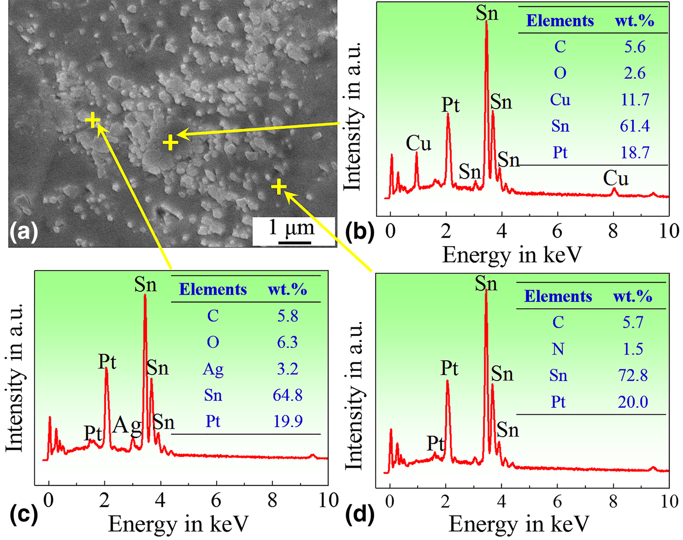
As mentioned previously, the content of Ag and Cu in this solder alloy is so low that the IMCs are difficult to detect by the XRD. Hence, SEM and EDS are utilized here to confirm these IMCs. The secondary electron images with EDS patterns of the 334.0 µm droplet are shown in Fig. 4. Insets are weight fraction of elements. In addition to the Sn, Ag, and Cu, some other elements are also detected. C, N, and O may result from the contamination on sample while Pt comes from the conducting coating. Micro-sized, round-shaped phases are observed in Fig. 4(a). In Fig. 4(b), Cu and Sn are simultaneously detected. In Sn0.3Ag0.7Cu, Cu cannot solute in the Sn matrix, while Cu6Sn5 is the dominant phase containing Cu element.[Reference Fu, Song, Hu, Chai, Feng and Wang22] Consequently it is concluded that the detection of Cu implies the formation of Cu6Sn5.[Reference El-Daly, El-Taher and Dalloul23] In addition, a large number of nano-sized particles are distributed in the matrix. Sn and Ag elements are enriched in these particles. In SnAgCu solder, nearly all the Ag element is enriched in Ag3Sn.[Reference Sundelin, Nurmi, Lepistö and Ristolainen11, Reference Gong, Liu, Conway and Silberschmidt24] So, these particles with Ag element are deemed as the Ag3Sn,[Reference El-Daly, El-Taher and Dalloul23] as displayed in Fig. 4(c). According to the equilibrium binary phase diagram of Sn–Ag,[Reference Kattner19] there is a negligible solid solubility of Ag in Sn. Consequently, only Sn is detected in the matrix, as indicated in Fig. 4(d). One may note the discrepancy between nominal composition and EDS results in Fig. 4. This is mainly caused by the following two factors. Compared with the micro-sized Sn matrix, IMCs are at nanoscale. EDS results are significantly interfered by the size discrepancy. Additionally, C, N, and O were detected, affecting quantitative analysis on the IMCs.
Secondary electron image and EDS results of the 334.0 µm droplet. (a) The solidification structure of 334.0 µm droplet. (b–d) EDS patterns of micro-sized, nano-sized particles, and matrix, respectively. The insets are the weight percent composition of each element. Due to the organic residues from abrasive paper and resin, C (Kα 1 = 0.277 keV), N (Kα 1 = 0.392 keV), and O (Kα 1 = 0.525 keV) are detected in the EDS pattern.

In the rapid solidification of Sn0.3Ag0.7Cu alloy, primary β-Sn precipitates firstly from the melt and it is the dominant matrix phase in the microstructure. Both Cu and Ag are expelled from the β-Sn phase and they aggregate in the interface between β-Sn and the melt. After the primary crystallization of β-Sn, the solubility of Cu in melt decreases as temperature reduces. Once the maximum solubility is reached, Cu begins to precipitate in the form of Cu6Sn5. With the assumption of Cu element, the concentration of Ag in the interface increases as temperature further drops. Similarly, Ag precipitates as well in the form of Ag3Sn. Because of the high cooling rate, the nucleation of Ag3Sn and Cu6Sn5 is largely promoted, while their growth is seriously suppressed. Consequently, refined solidification structure is observed. According to Sn–Ag–Cu phase diagram and corresponding isothermal sections at different temperatures,[Reference Kattner19, Reference Swenson25, Reference Moon, Boettinger, Kattner, Biancaniello and Handwerker26] a monovariant binary eutectic reaction occurs following primary β-Sn to produce eutectic Cu6Sn5 + β-Sn. As temperature further decreases, β-Sn, Ag3Sn, and Cu6Sn5 are produced by invariant eutectic reaction. Below the eutectic point, Cu cannot act as the solute in the matrix of Sn, while some Ag atoms can be trapped on rapid solidification. With continuous reduction of temperature, Ag3Sn precipitates from Sn matrix attributing to the decrease of solid solution. Compared with Cu6Sn5 particles, which are completely produced in eutectic reaction, the growth time for Ag3Sn particles precipitating from Sn is cut short. Additionally, it is suggested that Cu exhibits higher mobility in Sn.[Reference Ye, Lai, Liu and Thölén27, Reference Kao, Lin and Duh28] Both aspects contribute to the difference in the grain size between the Ag3Sn and Cu6Sn5. Apart from the external cooling rate, the different driving forces of growth play important roles in determining the particle size. Improved mechanical properties are expected in this solder droplets attributing to the optimized internal structure, which is especially crucial for direct structuring, such as 3D printing.
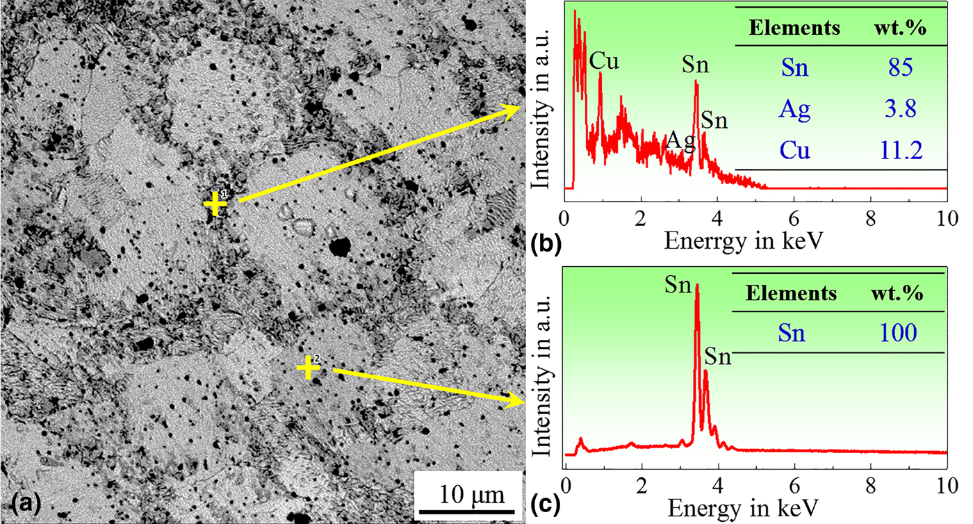
Figure 5(a) show the backscattered electron image with EDS patterns. Corresponding EDS results of the precipitates and matrix are shown in Figs. 5(b) and 5(c), respectively. In Fig. 5(a), there are precipitates in the boundaries of the β-Sn. As indicated in Fig. 5(b), both Cu and Ag are detected in these precipitates, which further verifies the results indicated by Fig. 4. In the solidification of Sn0.3Ag0.7Cu alloy, the grain boundaries provide nucleation sites for the Ag3Sn and Cu6Sn5 IMCs, resulting in their enrichment around the grain boundary areas. In this study, the IMCs precipitated in the grains are seldom detected because the IMCs precipitates along certain crystallographic orientation.[Reference Gong, Liu, Conway and Silberschmidt29]
Backscattered electron image and EDS results of droplet. (a) Microstructure of solder droplet in backscattered electron mode. (b, c) EDS patterns of the precipitations and matrix, respectively. The composition obtained by EDS is displayed in the inset.

Conclusions
In this study, we have used the POEM approach to prepare Sn0.3Ag0.7Cu droplets with powder diameter ranging from 70.6 to 334.0 µm. These droplets possess narrower size distribution and spherical shape without notable satellite particles. Furthermore, the POEM approach provides high cooling rate, which refines the microstructure of the droplets. Microstructure analysis shows that nano-sized Ag3Sn and Cu6Sn5 particles are finely distributed in the β-Sn matrix in the droplets prepared.
Acknowledgments
This work is supported by Program for Professor of Special Appointment (Eastern Scholar) at Shanghai Institutions of Higher Learning (No. TP2014042), People's Republic of China, the National Natural Science Foundation of China (Numbers 51171105 and 51671123), Natural Science Foundation of Liaoning Province (No. 2013020114), 085 project in Shanghai University, People's Republic of China, and Open Fund of Shanghai Key Laboratory of Digital Manufacture for Thin-walled Structures, People's Republic of China.