I. INTRODUCTION
Two-dimensional (2D) crystals and layered transition metal dichalcogenide (TMDC) systems, in recent times, have gained significant attention due to the virtue of their extraordinary properties, specifically related to light matter interaction. Reference Novoselov, Jiang, Schedin, Booth, Khotkevich, Morozov and Geim1–Reference Radisavljevic, Radenovic, Brivio, Giacometti and Kis4 Molybdenum disulphide (MoS2), similar to several other TMDC semiconductors, has attracted substantial interest due to its special properties that might lead to several photonics based applications. Reference Ghosh, Najmaei, Kar, Vajtai, Pradhan, Lou, Balicas, Ajayan and Talapatra5–Reference Ghosh, Winchester, Muchharla, Wasala, Feng, Elias, Krishna, Harada, Chin, Dani, Kar, Terrones and Talapatra11 The presence of a direct band gap in single layer MoS2 and the observation of strong photoluminescence is, to date, lauded as some of the most fascinating properties of this material. Investigations on other members of the TMDC family, for example, MoSe2, WS2, WSe2, InSe2, etc., indicate that one to a few layers of 2D-TMDCs can play a crucial role in applications related to optoelectronics ranging from fast photo-switches to solar cells. With a range of investigations pointing toward the possible potential of these materials for future applications, it is slowly becoming clear that some of the niche properties of TMDC materials also depend on a variety of other factors such as, the dielectric environment, the nature of the supporting substrates, etc. For example, in one of the initial studies, it was shown that multilayer MoS2 field effect transistors (FETs) on SiO2 mostly exhibited unipolar, n-type behavior with mobilities ∼30–60 cm2/V s, independent of the SiO2 thickness. However, multilayer MoS2 FETs fabricated on polymer substrates, such as polymethyl methacrylate, exhibited ambipolar behavior with electron and hole mobilities reaching ∼480 cm2/V s in relation to increasing polymer thickness. Reference Bao, Cai, Kim, Sridhara and Fuhrer12
Such a behavior, as several other investigations have indicated, is not restricted only to electronic properties, but also extends to other important physical properties as well. It was recently shown that the vibrational properties of MoS2 crystals grown (using sulfurization of MoO2) on SiO2 substrates are quite different from those that were grown on quartz substrates. Reference Bilgin, Liu, Vargas, Winchester, Man, Upmanyu, Dani, Gupta, Talapatra, Mohite and Kar13 One of the initial studies in this field revealed that the Raman and photoluminescence (PL) emission from single-layer MoS2 depends significantly on the underlying substrate. In this study a variety of underlying dielectric and conducting substrates were used and it was shown that the absorption as well as emission properties of monolayer MoS2 are strongly modulated by interference effects within different substrates. Reference Buscema, Steele, van der Zant and Castellanos-Gomez14 On similar grounds, it was recently shown that it is extremely simple to control the photonic and electronic properties of thin layer tungsten selenide (WSe2) by controlling the thickness of the underlying substrate. Reference Lien, Kang, Amani, Chen, Tosun, Wang, Roy, Eggleston, Wu, Dubey, Lee, He and Javey15 Thus it is clear that the properties of a few atomic layers of 2D TMDCs are greatly affected by the underlying substrate as well as their heterostructures. Now tremendous effort is being devoted to create and characterize a variety of heterostructures using 2D layered TMDCs. For example, the growth and exotic properties of heterostructures involving WS2/MoS2, graphene/hexagonal boron nitride (BN), MoS2/graphene, WS2/BN, etc. are already demonstrated. Reference Gong, Lin, Wang, Shi, Lei, Lin, Zou, Ye, Vajtai, Yakobson, Terrones, Terrones, Tay, Lou, Pantelides, Liu, Zhou and Ajayan16–Reference Zhang, Meng, Christianson, Arroyo-Torres, Lukowski, Liang, Schmidt and Jin20
Understanding substrate specific interactions and their effect on the structure and properties of 2D layered semiconductors and their heterostructures, is therefore, becoming essential to develop them for future functional applications. In this article, we report on the photo-response studies of MoS2–BN heterostructures grown on (001)-oriented Si substrates. We investigated vertical heterostructures consisting of ∼20 nm of MoS2 deposited on BN layers of a thickness of ∼35 and ∼80 nm (using precalibrated values). These samples will be classified as 20MoS2/35BN and 20MoS2/80BN from now on. We found that upon illuminating the devices using a continuous laser of λ = 658 nm (E = 1.88 eV) with a scaled laser intensity P ∼10 μW, under high vacuum, the steady state photocurrent (I ph) of 20MoS2/80BN samples was found to be ∼120 nA, which was 4 times more than the values obtained from 20MoS2/35BN samples. The variation of I ph on P was found to be super linear (I ph ∝ P γ) with γ = 1.04 in 20MoS2/35BN and γ = 1.07 in 20MoS2/80BN over the whole range of laser intensities studied (∼1 μW < P < 10 μW). Within the same range of intensities, the responsivity values obtained for 20MoS2/80BN ∼12 mA/W was an order of magnitude higher than the 20MoS2/35BN. We further investigated several devices fabricated from the sample with higher responsivity values (20MoS2/80BN) under ambient conditions with the same laser source and at P = 10 μW. Under ambient conditions the value of responsivity was found to be substantially smaller (∼1 mA/W) for these devices. A detailed discussion pertaining to the photocurrent behaviors seen in our experiments is also presented.
II. MATERIALS AND METHODS
Large area MoS2–BN heterostructures were grown on (001)-oriented Si substrates with radio frequency (RF) magnetron sputtering using a multi-target AJA-300 high vacuum sputter deposition system (base pressure ∼5 × 10⁻⁸ Torr) (AJA International, North Scituate, Massachusetts). Commercially available MoS2 (99.95% purity) and BN (99.9%) were used. Argon was used as the process gas for the MoS2 layer, while an Ar:N2 (5:1) mixture was preferred for the BN layer. Both layers were deposited at 350 °C.
The layered heterostructure calibration and detailed structural analysis were performed using an x-ray reflectivity (XRR) technique (Phillips MRD, PANalytical, Boulder, Colorado) with a Cu Kα-source. Fitting to the XRR data was performed using the GenX software. Reference Björck and Andersson21
Micro-Raman spectroscopy analysis of the samples grown by the sputter deposition of MoS2 films on SiO2 and BN substrates was performed utilizing a Renishaw inVia confocal microscope-based Raman spectrometer (Renishaw, Hoffman Estates, Illinois) using a 514.5 nm excitation wave length. Raman spectroscopic characterization was performed under ambient conditions with a backscattering geometry. The laser power was kept below 1.5 mW to prevent the damage on the samples. The laser spot size was maintained about 2 µm utilizing a 50× objective lens.
For performing electrical and photocurrent measurements, Chromium (Cr)/Gold (Au) (20 nm Cr/100 nm Au) contact pads were deposited on MoS2/BN heterostructures using thermal evaporation of these metals through a shadow mask [transmission electron microscope (TEM) grid]. The samples were then mounted on a chip holder inside a close cycle helium cryostat with an optical window and the system was pumped down to a high vacuum level (∼10−6 Torr) before performing the electrical and optical measurements. Current–voltage (I–V) measurements were performed using Keithley source meters (2400 series; Keithley Instruments Inc., Cleveland, Ohio) and the photo-response properties of these samples were investigated using a continuous wave solid-state laser system [wave length λ = 658 nm (E = 1.88 eV)].
III. RESULTS AND DISCUSSION
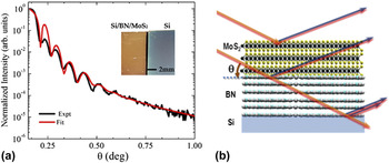
Results of structural characterization of one of the heterostructures, 20MoS2/35BN, are presented in Fig. 1. The XRR reflectivity curve of this sample is shown (solid black). We would like to note that for quantitative roughness estimation we have utilized XRR for the following reasons. XRR is one of the widely used techniques for providing roughness information for a large area specimen quickly, which typically is not possible using atomic force microscopy (AFM) or scanning electron microscopy (SEM). Further, interface roughness can also be characterized using XRR, which is a major advantage compared to both AFM and SEM.
(a) XRR data of the 20MoS2/35BN sample, showing XRR fringes indicative of the presence of sharp interfaces in these heterostructures. The inset shows the optical image of the deposited 20MoS2/35BN heterostructure and blank Si substrate. (b) Possible existence of these interfaces.

Clear XRR fringes are observed in the data, which indicates that these multi-layers have reasonably sharp interfaces. A fit analysis of these data was performed to extract the thickness, roughness, and density of all the constituent layers (red curve). Apart from BN and MoS2 layers, we found evidence of a rough, chemically mixed layer at the Si–BN interface in the samples. Without considering the existence of these layers, the goodness-of-fit was much higher than desirable. Even though the chemical composition of these layers cannot be quantified through this analysis, the fit density and scattering factor value are consistent with an oxy-nitride layer of Si and B at the Si–BN interface. This is not surprising since a native oxide layer of Si, and the presence of N2 during BN deposition accentuates the nitride phase. The values of thickness and roughness of these interfacial layers obtained from our XRR investigations for both samples are provided in Table I. Apart from the presence of these interfacial layers, we also find a lower MoS2 average density (compared to the bulk value) and small deviations from the nominal 1:2 MoS2 stoichiometry within the sample area. However, Raman spectroscopy measurements performed on our samples showed clear evidence that the MoS2 phase was present.
Parameters extracted from XRR reflectivity measurements are listed.

Raman spectroscopic investigations are routinely used to identify layered MoS2 structures.
Reference Windom, Sawyer and Hahn22–Reference Boukhicha, Calandra, Measson, Lancry and Shukla25
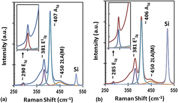
The data from the Raman measurements performed on 20MoS2/35BN and 20MoS2/80BN heterostructures are shown in Figs. 2(a) and 2(b), respectively. Multiple Raman spectra, with a laser exposure time of ∼120 s, were collected from several areas of the samples to validate the reproducibility of the data as well as the uniformity of the deposited samples. The Raman spectra showed signatures of vibrational modes related to MoS2. Two of the most prominent peaks, around 381 and 407 cm−1, were observed in the Raman data for both the samples and can be, respectively, assigned to the first-order
 ${\rm{E}}_{2{\rm{g}}}^1$
and A1g modes at the Γ-point of the hexagonal Brillouin zone of 2D-MoS2.
Reference Ghosh, Winchester, Muchharla, Wasala, Feng, Elias, Krishna, Harada, Chin, Dani, Kar, Terrones and Talapatra11,Reference Bilgin, Liu, Vargas, Winchester, Man, Upmanyu, Dani, Gupta, Talapatra, Mohite and Kar13,Reference Windom, Sawyer and Hahn22–Reference Boukhicha, Calandra, Measson, Lancry and Shukla25
A broad peak around 450 cm−1 was also observed, which could be due to the second order longitudinal acoustic phonons near the M-point of the Brillouin zone [2LA(M)], often observed in multiple layers of MoS2. Further, a sharp peak, around 285 cm−1, was observed [see the inset of Figs. 2(a) and 2(b)]. This peak is generally associated with E1g phonons near the Γ-point and was recently observed in multilayer samples grown using direct vapor-phase sulfurization of MoO2 on SiO2/Si as well as quartz substrates.
Reference Bilgin, Liu, Vargas, Winchester, Man, Upmanyu, Dani, Gupta, Talapatra, Mohite and Kar13
(a) Raman spectrum obtained from the 20MoS2/35BN sample. Several vibrational modes akin to MoS2 layers are identified in this spectrum. The inset shows the presence of E1g mode ∼290 cm−1 in these samples. (b) The Raman spectrum obtained from the 20MoS2/80BN sample. The inset shows the presence of E1g mode ∼285 cm−1 in these samples. The peak observed at 520 cm−1 in both these spectra belongs to the Si substrate on which these heterostructures were fabricated.

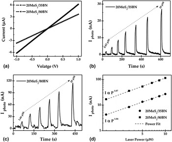
We next investigated the photo-current response properties of the MoS2/BN heterostructures. Before performing the photo-switching experiments, current–voltage (I–V) characteristics of these devices were measured in a two probe configuration. The samples were between the two contact electrodes, biased up to ±1 V, for performing the I–V measurements. Figure 3(a) shows the I–V curves obtained from typical heterostructures (without any light illumination). I–V curves for both the structures were found to be linear in nature. This indicated that good ohmic contacts persisted between the MoS2 channel and the metal electrodes within the applied voltage regime. The linearity of I–V curves without illumination was tested to show that within the applied voltage regime, under which the measurements were performed, the contacts were able to replenish the carriers when they are drawn out from the material under an applied electric field. We found that the channel current is slightly increased with the increase in the thickness of the bottom BN layer.
(a) Linear current–voltage (I–V) response obtained from 20MoS2/35BN and 20MoS2/80BN samples is shown. (b) Room temperature photo-switching behavior of 20MoS2/35BN under laser illumination of λ = 658 nm at different laser powers ∼0.8–10 μW is shown. (c) Similar data, as shown in (b) are presented for 20MoS2/80BN. (d) Shows the variation of I ph with laser intensity (at 10 μW) for both these samples. The dotted line in this figure indicates power fit to the data plotted on a double logarithmic scale. The measurements for all the data presented in this figure were performed at room temperature and under high vacuum (∼10−6 Torr).

In Figs. 3(b) and 3(c), the photo-switching characteristics of MoS2/BN heterostructures at different laser intensities are shown. A source–drain voltage of 1 V was applied between the electrodes of the devices being measured and the laser intensity was varied from ∼1 to 10 μW (scaled value of laser power according to the device area). The photo-switching measurements were performed in the following way. The device was continuously biased with 1 V without turning the laser ON and the current (I dark) was recorded. Subsequently, the laser intensity was fixed at a specific power and was switched ON for about 10 s, during which the evolution of the current (I ill) was recorded. This sequence was followed for the photo-response of these devices for several laser intensities. Between each “laser ON” sequence we waited until the channel current reached its initial I dark value (about 20–30 s). The photo-current (I ph) is the current obtained by subtracting the current under illumination from the current obtained under dark conditions at different laser intensities (I ph = I ill − I dark).
In Fig. 3(d), dependence of I ph on laser power (P) is presented. In this figure, I ph as a function of P is plotted in a double logarithmic scale. The data obtained seems to fit very well with a power law dependence of the form I ph ∝ P γ, where γ = 1.04 and γ = 1.07 for 20MoS2/35BN and 20MoS2/80BN heterostructures, respectively. This behavior is surprisingly different from most of the studies reported so far in the literature. Typically, in highly crystalline materials, the value of γ = 0.5 corresponds to bimolecular processes, or γ = 1 corresponds to monomolecular processes. Reference Rose26 These processes are often observed in semiconducting systems with few trap states. Power exponents with values of γ ranging between 0.5 and 1 (0.5 < γ < 1.0) are also very common in disordered semiconductors and in chalcogenide glasses. Reference Rose26–Reference Mott and Davis30 In the absence of the photo-phenomenon arising from photo-gating artifacts, thermoelectric effects and so on, fractional dependence of the power exponent seen in a variety of systems was explained on the basis of a theoretical model which assumes an exponential distribution of trap states in the mid-gap state. Reference Rose26 Such fractional distribution was recently observed for thin film photo-detectors fabricated using liquid phase exfoliated MoS2 materials. Reference Ghosh, Winchester, Muchharla, Wasala, Feng, Elias, Krishna, Harada, Chin, Dani, Kar, Terrones and Talapatra11
However, a few reports on the super linearity of power exponent γ in several systems have been reported in the past. Reference Kushwaha, Kushwaha, Shukla and Kumar31,Reference Bakr32 Though to date a clear theoretical understanding of such a phenomenon is still lacking, a few have tried to explain it on the basis of the presence of recombination centers with different energies and capture cross-sections. Reference Rose26 More recently, such super linear dependence of I ph over a broad range of laser power was also observed in a variety of compositionally different MoS2 and MoSe2 systems Reference Klee, Preciado, Barroso, Nguyen, Lee, Erickson, Triplett, Davis, Lu, Bobek, McKinley, Martinez, Mann, Talin, Bartels and Léonard33 and was explained on the basis of a model, which considered the presence of three types of recombination centers in the samples studied. Whether a similar model can be applied to explain the behavior seen in our experiments or some other, more complicated, phenomenon is responsible for the super linearity of the γ observed in the MoS2/BN heterostructures, is, at present, beyond the scope of this article and will be investigated in greater detail in the future.
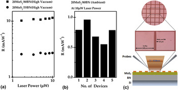
We also calculated the responsivity values of these samples at different laser powers. Responsivity (R) is defined as R = I ph/P light (where P light is the power of the incident light), and is an important performance factor used for quantifying the effectiveness of photoactive materials. Figure 4(a) shows the room temperature responsivity of the MoS2/BN heterostructures measured under high vacuum (∼10−6 Torr) at different laser powers. The responsivity at 10 μW was found to be ∼2.7 and ∼12 mA/W for 20MoS2/35BN and 20MoS2/80BN heterostructures, respectively. These responsivity values are several orders of magnitude greater than the responsivity of liquid exfoliated MoS2 thin film photodetectors ∼50 μA/W (Ref. Reference Ghosh, Winchester, Muchharla, Wasala, Feng, Elias, Krishna, Harada, Chin, Dani, Kar, Terrones and Talapatra11) as well as chemical vapor deposition (CVD) grown multilayer WS2 based devices ∼22 μA/W. Reference Perea-López, Elías, Berkdemir, Castro-Beltran, Gutiérrez, Feng, Lv, Hayashi, López-Urías, Ghosh, Muchharla, Talapatra, Terrones and Terrones27 Thus a very convincing evidence of the enhancement of photocurrent was observed with the increase in the underlying BN layer thickness in these heterostructure. Though, several factors can affect photocurrent generation in optically active semiconductors (e.g., presence of trap states), recent investigations show Reference Buscema, Steele, van der Zant and Castellanos-Gomez14,Reference Lien, Kang, Amani, Chen, Tosun, Wang, Roy, Eggleston, Wu, Dubey, Lee, He and Javey15 that underlying dielectric layer has profound effects on the optical properties of TMDCs. For example, it was hypothesized Reference Buscema, Steele, van der Zant and Castellanos-Gomez14,Reference Lien, Kang, Amani, Chen, Tosun, Wang, Roy, Eggleston, Wu, Dubey, Lee, He and Javey15 that due to the several layers present in these hetero-structures (e.g., MoS2, BN, and Si) absorbed light can undergo multiple reflections between the layer boundaries. As a result of these multiple reflections, constructive interference between absorption and emission of light occurs. Such effects can substantially alter the optical properties of the top layer materials. We believe that a similar phenomenon is perhaps responsible in the present case as well.
(a) Responsivities obtained for the samples 20MoS2/35BN and 20MoS2/80BN as a function of laser power is shown. These measurements were performed at room temperature under a high vacuum of ∼10−6 Torr. (b) Responsivities obtained for five different 20MoS2/80BN devices under ambient conditions. (c) Shows an optical micrograph of 20MoS2/80BN with contact pads on top along with a schematic of the two point probe arrangement used for the measurements to obtain the data shown in (b).

We further found that the responsivity values for these heterostructures drastically reduce when they are exposed to ambient conditions. For example, the measurement on several 20MoS2/80BN samples in the presence of air and with a laser illumination of 10 μW showed roughly an order of magnitude reduction in their responsivity (between 1 and 0.5 mA/W for five different devices measured) values. These results are presented in Fig. 4(b). Such reduction in responsivities is not surprising and is associated with the fact that MoS2 surfaces are extremely sensitive to the surrounding environmental conditions. Reference Qiu, Pan, Yao, Li, Shi and Wang34,Reference Park, Park, Jang, Lee, Jeong, Cho, Hong and Lee35 Specifically, channel current in MoS2 FETs deteriorates significantly under ambient conditions Reference Qiu, Pan, Yao, Li, Shi and Wang34 as well as in the presence of oxygen. Reference Park, Park, Jang, Lee, Jeong, Cho, Hong and Lee35 Such deterioration is caused by the electron capturing nature of adsorbed oxygen on the sulfur or defect sites of MoS2, which results in the reduction of the channel current. Reference Qiu, Pan, Yao, Li, Shi and Wang34 We anticipate similar processes occurring in our case as well.
IV. CONCLUSION
We have shown that the thickness of BN layers significantly affects the photocurrent response properties of MoS2 deposited on top of the layers. Our investigations show that an order of magnitude increase in photo-currents can be achieved in MoS2 layers by simply increasing the underlying thickness of BN from 35 to 80 nm. We have also observed unusual super linear dependence of photocurrent in these heterostructures over the range of laser intensities studied. Further measurements with several other thicknesses of the BN under layer are underway and will be published subsequently. These future measurements are needed to conclusively understand the exact science behind the photocurrent response behavior observed in a MoS2/BN system. Though our measurements specifically focused on MoS2 on BN, we believe that such an outcome, in general, is possible for a variety of other optically active 2D TMDC layered heterostructures. However, the present study shows some encouraging results for creating functional heterostructures using the sputtering technique on Si. We believe that this method is also applicable for large area growth on any other substrates and can be, in principle, expanded to synthesize a layered 2D heterostructure on flexible substrates (e.g., thin polymer sheets, etc.) as well. Tuning of optical properties of TMDCs through substrate specific engineering, as reported here, is extremely valuable to develop 2D layered heterostructures for a variety of electronic and optoelectronic based future applications.
ACKNOWLEDGMENTS
This work is supported by the U.S. Army Research Office through a MURI Grant No. W911NF-11-1-0362. The X-ray reflectivity experiment shown was carried out in the Frederick Seitz Materials Research Laboratory Central Research Facilities, University of Illinois. D.M. would like to acknowledge Dr. Mauro Sardela for his help with X-ray measurements.