Introduction
Conservation of the environment has become a critical issue for sustaining the well-being of humankind. One factor that threatens the environment is the soaring demand for electric power from fields, including transportation, information, and telecommunications. The established infrastructure for electric power distribution already represents a powerful network and is ready to grow toward smart grid implementation. However, an inexhaustible supply of electric power from nuclear power plants is now viewed as unrealistic, especially after the meltdown of the Fukushima nuclear power plant in Japan. As a result, drastic reduction of electric power loss during power distribution is necessary.
Power electronics systems manage alternating current-direct current (AC-DC) and DC-DC conversions between each stage of electric power distribution. Fundamental circuits (inverters and converters) for the power electronics systems consist of energy-storage components (inductors and capacitors) and switching components (semiconductor diodes and transistors), which alternate the conduction between the ON- and OFF-states. The efficiency of these power conversions is constantly being improved by limiting power losses in the components within power electronics systems.
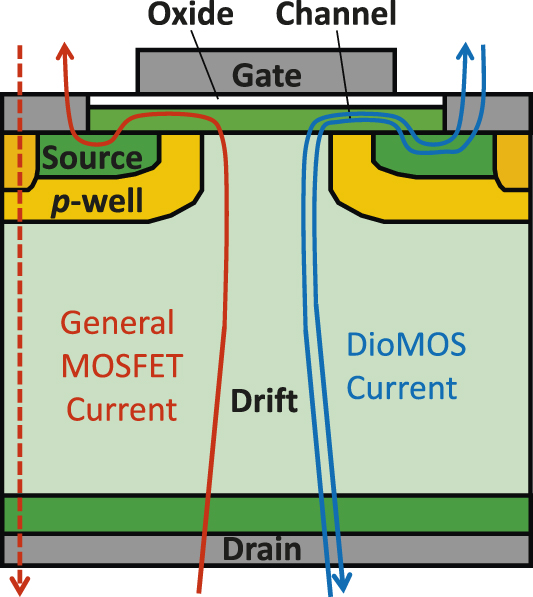
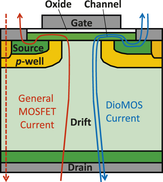
Figure 1 shows the unit structure of a typical vertical power metal oxide semiconductor field-effect transistor (MOSFET), which contains a planar MOSFET on the surface with a voltage-blocking drift layer under the MOSFET. Thousands of such units are typically integrated into power-device chips to manage large currents. Semiconductor power devices must withstand large voltages during the OFF-state by using a thick drift layer, which in turn causes conduction loss because of the large ON-state resistance (R ON). Additional power losses result from the switching period of these power devices, typically on the order of a few to hundreds of kHz.
Schematic cross-section of a vertical SiC power metal oxide semiconductor field-effect transistor (MOSFET).Reference Kitabatake11 Current flow paths are illustrated by red arrows on left side. The unipolar MOSFET current and the bipolar diode current are distinguished using solid and dashed lines, respectively, on the left side of the figure. The SiC diode-integrated MOSFET (DioMOS)Reference Uchida, Horikawa, Tanaka, Takahashi, Kiyosawa, Hayashi, Niwayama, Kusumoto, Adachi, Kudou and Kitabatake15 has a similar structure as the SiC MOSFET with the exception of the MOS-channel. The current flow paths of the DioMOS are illustrated by blue arrows on the right side of the figure. Both the MOSFET and diode currents follow the same path under unipolar conduction, as illustrated by the solid lines.
Conventional Si power devices with blocking voltages (BVs) >400 V take advantage of bipolar conductivity modulation (both majority carriers and minority carriers support the current conduction) to reduce the conduction loss of R ON from the thick drift layer. The Si insulated gate bipolar transistor (IGBT) with this bipolar conductivity modulation has become a more favorable solution compared to the unipolar Si MOSFET. On the other hand, bipolar conductivity modulation inevitably leads to slower turn-off switching due to excess minority carriers and larger switching losses.
Si power devices cannot be easily applied to modern applications requiring higher voltages, higher currents, lower conduction losses, and higher switching frequencies.Reference Jayant Baliga1 Silicon carbide (SiC), an emerging wide-bandgap semiconductor material, is deemed to be the solution to this problem, thereby allowing for the realization of low-loss power devices for next-generation power electronics systems. SiC consists of Si and C, both of which are abundant natural resources. Furthermore, general doping impurities N (n-type) and Al (p-type) are both environmentally friendly. The breakdown field for SiC, as compared to that for Si, is 10 times larger and allows for a thinner voltage-sustaining drift layer that is 10 times thinner and more concentrated, thus resulting in low conduction loss. The specific R ON for SiC is more than 10 times lower than that for Si. Unipolar SiC power devices without bipolar conductivity modulation can be used in applications where the BV is greater than 400 V. Unipolar SiC MOSFETs can overcome the tradeoff between conduction loss and switching loss that is well known in Si IGBTs.Reference Jayant Baliga1
SiC is a stable material with a very low impurity diffusion coefficient. In SiC, it is possible to form precisely controlled doped layers, better than Si, in order to design high-performance power devices permitted only for SiC. This article presents an example of a precisely controlled doped layer in SiC, enabling a low-loss diode-integrated SiC power MOSFETs.
SiC epitaxial growth
General developments
The history of the SiC wafer, including the development of epitaxial films of SiC, is filled with struggles to achieve a suitably low occurrence of the defects (such as poly-type inclusions, stacking faults, and dislocations), which do not commonly exist in commercial Si wafers.Reference Choyke, Matsunami and Pensl2 There exist many poly types (e.g., 4H, 6H, 3C) in SiC, with different stacking periodicity of Si-C bilayers; 4H-SiC represents the hexagonal crystal lattice with stacking periodicity of four Si-C bilayers. 4H-SiC wafers have been on the market for more than 20 years, and defect density and cost are steadily decreasing. Nevertheless on this stage, typical 4H-SiC wafers still include defect densities as high as 1000/cm2 (compared to almost zero in Si wafers), and the cost is more than 10 times as expensive as Si wafers. Recently, the diameter of commercially available 4H-SiC wafers has been increasing toward six inches (150 mm), which is larger than previous diameters of three and four inches (75 and 100 mm, respectively).
SiC power devices require high-quality crystalline drift layers that are epitaxially grown on SiC wafers. chemical vapor deposition (CVD) is commonly used for SiC epitaxial growth. In CVD, SiH4, C3H8, and H2 carrier gases are introduced into the CVD reactor, and the substrate temperature is set to 1500–1700°C. N2 gas is used for n-type doping. Typical substrates used for epitaxial growth include the 4H-SiC(0001) Si-face off-oriented wafers that are inclined four degrees toward the [11–20] direction. The off-oriented substrates ensure that the step-flow growth of 4H-SiC proceeds at each step edge without any other polytype (3C, 6H) formation on the (0001) terraces.Reference Matsunami and Kimoto3 Nevertheless, the off-oriented surfaces sometimes form rough step-bunching surfaces that have step heights greater than 10 nm.Reference Kitabatake, Sako, Sasaki, Yamashita, Tamura, Yamada, Ishiyama, Senzaki and Matsuhata4 Smooth surfaces with uniform—<1 nm—asperities are only achieved under optimized growth conditions.Reference Kamata, Tsuchida, Jikimoto and Izumi5 Much research is still on-going to determine the impact of step-bunching surfaces as well as defects carried over from the wafers on the power device performance and reliability.Reference Kitabatake, Sako, Sasaki, Yamashita, Tamura, Yamada, Ishiyama, Senzaki and Matsuhata4
SiC(0001) terrace surfaces are stabilized with additional Si atoms to form special surface reconstructions.Reference Kitabatake6,Reference Takahashi, Uchida and Kitabatake7 The additional Si atoms prefer sites where dangling bonds of three Si atoms on the (0001) terrace surface can be fulfilled. This reconstructed surface, which has a low density of dangling bonds, activates surface migration on the (0001) terraces and therefore is preferred for growing smooth surfaces with good crystallinity.Reference Kitabatake6,Reference Kitabatake8 The Si-rich surface is also known to promote high doping probability of N atoms, because N impurity atoms replace the C sites in the SiC crystalline lattice.Reference Larkin, Neudeck, Powell and Matus9
Precisely controlled doped layer
We have been developing a unique nanotechnology to form highly doped (greater than 1018 cm3) and ultrathin (less than 50 nm) layers during SiC epitaxial growth.Reference Takahashi, Yokogawa, Uchida, Kusumoto, Yamashita, Miyanaga and Kitabatake10 Gas flow in the CVD reactor is carefully designed to replace the deposition species quickly and efficiently during epitaxial growth. N2 doping gas is switched on and off rapidly during epitaxial growth for an abrupt change in the doping concentration. The abrupt change in the doping concentration enables advanced design of the SiC devices. The epitaxial conditions, which are optimized to keep additional Si stabilized on the 4H-SiC(0001) surface, result in the growth of a highly doped layer with a smooth surface.
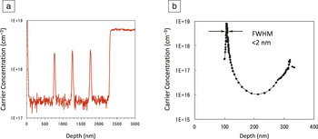
Figure 2a shows the depth profile of the N-concentration in a precisely controlled doped layer analyzed by secondary ion mass spectroscopy measurements. Three clearly separated periodic ultrathin (less than 50 nm) doped layers are observed in this sample. Figure 2b shows another example of a precisely controlled doped layer that exhibits a layer thickness ∼2 nm full width at half maximum, with peak concentration of 1 × 1019 cm–3, more than three orders of magnitude higher than the surrounding layers.Reference Takahashi, Yokogawa, Uchida, Kusumoto, Yamashita, Miyanaga and Kitabatake10 We have introduced these nm-level-controlled doped layers into the 4H-SiC MOSFET channel and have reported their remarkable device characteristics.Reference Kitabatake11 Since the N impurity atoms in the SiC crystalline lattice are slow to diffuse even at high temperatures (diffusion coefficient is less than 10–10 cm2/s at 2000°C in SiC, which is several orders of magnitude lower than that in Si).Reference Soloviev, Gao, Khlebnikov, Khlebnikov and Sudarshan12 The precisely controlled nm-scale thickness doped layers can only be realized in SiC using the technique described above and are stable during the device fabrication process and after repeated cycles of device operation while such impurity diffusion is not neglected in Si.
Depth profile of the carrier concentration in precisely controlled doped layers.Reference Takahashi, Yokogawa, Uchida, Kusumoto, Yamashita, Miyanaga and Kitabatake10 (a) Secondary ion mass spectroscopy profile of three ultrathin and highly doped layers. (b) The thinnest and most-doped layer as confirmed by the capacitance-voltage measurement. The profiles confirm an N-doped layer with a concentration as high as 1019 cm–3 and a full width at half maximum (FWHM) as thin as 2 nm.

SiC power devices
General developments
Much effort has been expended for the development of SiC MOSFETs. The vertical SiC MOSFET shown in Figure 1 is a common power device with an OFF-state BV~600–3300 V and an ON-state current of 10–100 A. The fabrication process begins with epitaxial growth of the weakly n-type drift layer, whose typical thickness and doping concentration are on the order of 10 μm and 1016 cm–3 for a BV∼1000V, respectively. The p-well and n +-source areas are formed by ion implantation of Al and N, respectively, followed by >1700°C high-temperature anneal to activate the dopant. The MOSFET channel is then formed on the implanted surface, where additional epitaxial growth is used to promote the formation of a smooth gate oxide interface.Reference Kitabatake11 High-temperature oxidization follows to grow the gate oxide, forming the MOS interface. The SiC-MOS interface typically exhibits problems such as low mobility and poor reliability. A post-oxidation anneal with NO and N2O gases are known to improve the SiC-MOS interface quality.Reference Chang, Porter, Bentley, Lu and Cooper13
In a vertical power MOSFET, a positive bias voltage is usually connected to a drain (bottom) against source (top) contact, and the ON-state “MOSFET current” flows from drain to source, as illustrated by the solid red arrow in Figure 1. The power MOSFET occasionally operates as a diode when negative voltage is applied to the drain in the power electronics circuit, and the “diode current” flows from source/p-well contact to the drain contact, as illustrated by the red dotted arrow in Figure 1. The conduction paths for “MOSFET current” and “diode current” are different. This “diode current” through the p/n junction between p-well and n-drift regions results in large conduction losses due to the wide bandgap nature of SiC. The bipolar p/n junction “diode current” in SiC power devices has been investigated, revealing severe R ON degradation through further defect degradation.Reference Skowronski and Ha14 To avoid these problems, a SiC Schottky barrier diode is usually used in parallel, which inevitably results in an increase in the total number of SiC chips, material cost, mounting area, and wiring inductances.
SiC diode-integrated SiC MOSFET
We have demonstrated SiC epitaxial growth of precisely controlled doped layers and its application to the MOSFET channel to form the diode-integrated MOSFET (DioMOS).Reference Uchida, Horikawa, Tanaka, Takahashi, Kiyosawa, Hayashi, Niwayama, Kusumoto, Adachi, Kudou and Kitabatake15,Reference Ohoka, Horikawa, Kiyosawa, Sorada, Uchida, Kanzawa, Sawada, Ueda and Fujii16 The proposed DioMOS has a basic device structure that is similar to that of conventional vertical power MOSFETs (Figure 1), except now the MOSFET channel consists of an ultrathin and highly doped n-type epitaxial layer. The epitaxial channel conducts both “MOSFET current” and “diode current,” as illustrated by the blue arrows on the right hand side of Figure 1. Both currents are carried by majority carriers, resulting in unipolar conduction that enables fast switching speeds without R ON degradation.
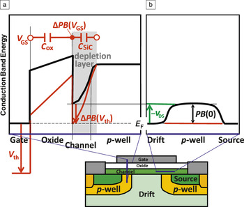
The operating mechanism of the DioMOS can be discussed using the conduction band energy plots along the vertical and horizontal directions of the channel in Figure 3. In these plots, the black lines illustrate the gate-source, and source-drain contacts when they are set to 0 V. Along the vertical direction plot shown in Figure 3a, the conduction band energy decreases in the channel region from the p-well and has a minimum at the oxide/channel interface because of charge in the depletion layer between the n-type channel and the p-well. The higher doping concentration in the channel results in a steeper decline compared to that of a lower channel concentration. The height of the energy minimum is a function of the doping concentration and thickness of the channel layer. This height with respect to the semiconductor Fermi level (E F) is the potential barrier (PB) between the drift layer and source in the horizontal-section plot shown in Figure 3b. PB is a function of the gate-source voltage (V GS) and expressed as PB(V GS). In order to ensure a normally-OFF operation under V GS = 0 V, PB(0)>0 above the p-well.
Conduction band energy plots of the metal oxide semiconductor (MOS)-channel of the SiC diode-integrated metal oxide semiconductor.Reference Uchida, Horikawa, Tanaka, Takahashi, Kiyosawa, Hayashi, Niwayama, Kusumoto, Adachi, Kudou and Kitabatake15 (a) Vertical-direction energy plot along the vertical direction illustrated by the blue line on the left side of the device figure. Depletion layer at the n-channel/p-well interface is colored gray. The conduction band energy when V DS = V GS = 0 is illustrated by black lines. Those cases for V GS = V th are illustrated by red lines, and the potential drops at the gate and the MOS interface are also indicated by red arrows. Thickness and doping concentration of the depletion layer affects the PB and the V th. (b) Horizontal-direction energy plot along the horizontal blue line illustrated on the right side of the figure. The potential rise in the drift region under the –V DS bias is indicated by the green line and arrow. When –V DS = PB(0), diode current starts to flow. Note: V DS, drain-source bias; V GS, gate-source voltage; V th, threshold voltage; PB, potential barrier; C ox, gate oxide capacitance; C SiC, SiC depletion-layer capacitance.

The diode operation of DioMOS can be understood as follows. Application of the –V DS (negative drain-source bias) increases the energy level within the drift region, and the effective potential barrier PB(0)–V DS seen by the electrons in the drift region gradually decreases, as illustrated by the green line in Figure 3b. Hence, electrons overcome the potential barrier and form the diode current.
MOSFET operation can be understood as follows. The applied positive gate bias V GS is dropped across two capacitors: the SiC depletion-layer capacitance (C SiC) and the gate oxide capacitance (C ox), as illustrated in red on upper part of Figure 3a. The change in potential barrier ΔPB(V GS) at the oxide/channel interface from V GS = 0 V to a nonzero gate bias value V GS is expressed using the simple capacitive divider circuit:
 $$\Delta PB{\rm{(\ }}{V_{{\rm{GS}}}}{\rm{)\ = \ }}PB{\rm{(0) - }}PB{\rm{(}}{V_{{\rm{GS}}}}{\rm{)\ = \ }}{V_{{\rm{GS}}}}{\rm{\cdot[}}{C_{{\rm{ox}}}}{\rm{\ /(}}{C_{{\rm{SiC}}}}{\rm{\ + \ }}{C_{{\rm{ox}}}}{\rm{)]}}{\rm{.}}$$
The red plots in Figure 3a– b show the energy plot when V GS = V th (threshold gate voltage) when the potential barrier becomes PB(V th) = 0 and the ON-state MOSFET current starts to flow. Substituting this into (1), the relationship between PB(0) and V th can be expressed as
 $$PB{\rm{(0)\ = \ }}{V_{{\rm{th}}}}{\rm{\cdot[\ }}{C_{{\rm{ox}}}}{\rm{/(\ }}{C_{{\rm{SiC}}}}{\rm{\ + \ }}{C_{{\rm{ox}}}}{\rm{\ )\ ]}}{\rm{.}}$$
It is generally preferable for power devices to have high V th for safe operation, preventing false turn-on during high-speed switching. In DioMOS, along with the high V th requirement, it is also preferred that the diode current exceeds the low PB to maintain low R ON conduction loss. Since it is desirable to have small PB(0) while maintaining high V th, C SiC must be designed to be as large as possible from Equation 2. Large C SiC and small PB(0) can be obtained with an appropriate depletion layer with a highly doped ultrathin channel and a highly doped p-well. A SiC DioMOS with PB < 0.8V and V th > 4.0V is therefore only achieved by using the precisely controlled SiC epitaxial growth technique. A typical n-type doped channel is designed for concentrations as high as 1018 cm–3 and thicknesses ∼30 nm. The doping concentration of the p-well is also designed to be on the order of 1019 cm–3. The low PB attained in the DioMOS is much smaller than that of the SiC p/n junction and similar to or even smaller than commercially available SiC Schottky barrier diodes for low loss diode current operation. Both diode current and MOSFET current are perfectly unipolar, which ensures safe power device operation. The DioMOS, which can be achieved with SiC, successfully integrates diodes and MOSFETs without an increase in chip size.
Electrical characteristics of SiC-DioMOS
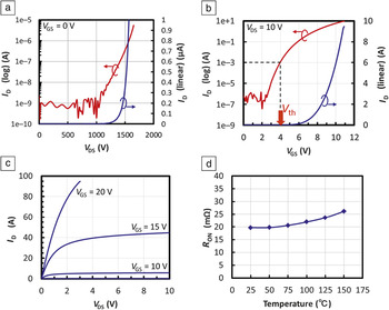
MOSFET operation of a successfully fabricated SiC DioMOS is shown in Figure 4.Reference Ohoka, Horikawa, Kiyosawa, Sorada, Uchida, Kanzawa, Sawada, Ueda and Fujii16Figure 4a shows the OFF-state drain current (I D) as a function of V DS (positive bias voltage to drain from source) when V GS is set to 0 V. The I D–V DS data confirms BV > 1600 V with avalanche breakdown and OFF-state leakage current <1 μA when V GS = 0 V. Figure 4b shows I D–V GS (positive bias voltage to gate from source) characteristics with V th = 4.0 V (V GS at I D = 1 mA). Figure 4c shows ON-state I D–V DS characteristics as a function of V GS showing low R ON of 20 mΩ under V GS = 20 V. The specific R ON is maintained as low as 4.7 mΩcm2. The DioMOS shows only a small variation of R ON over a wide range of temperatures, as plotted in Figure 4d, compared to the large increase of R ON observed under high temperatures in typical unipolar diodes and MOSFET devices. This is due to a balance between two opposing temperature dependences; one is the positive temperature dependence of the drift resistances with increased phonon scattering. The other is the negative temperature dependence for the channel resistance due to carrier detrapping at the SiC-MOS interface.
Electrical characteristics of metal oxide semiconductor field-effect transistor (MOSFET) current in the SiC diode-integrated MOSFET.Reference Ohoka, Horikawa, Kiyosawa, Sorada, Uchida, Kanzawa, Sawada, Ueda and Fujii16 (a) OFF-state I D-V DS characteristics. (b) I D-V GS characteristics. (c) ON-state I D-V DS characteristics. (d) Temperature dependence of the ON resistance R ON. Blocking voltage >1600 V, V th = 4.0 V, R ON = 20 mΩ, and a stable R ON in a wide temperature range are confirmed. Note: I D, drain current; V DS, drain-source voltage; V GS, gate-source voltage.

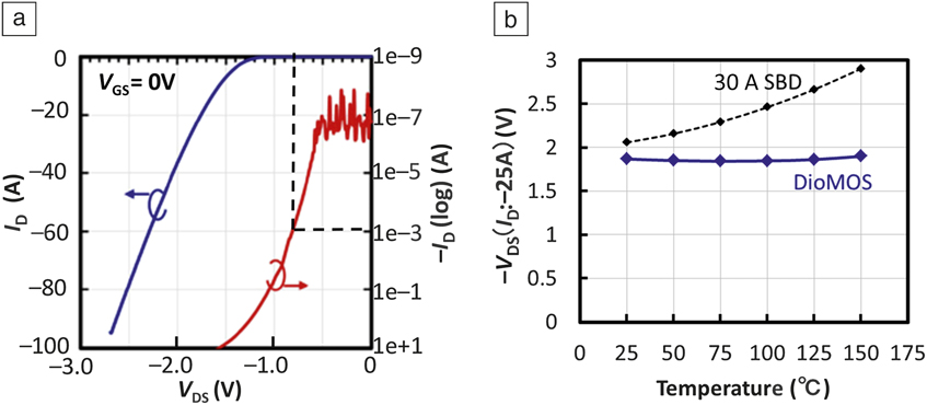
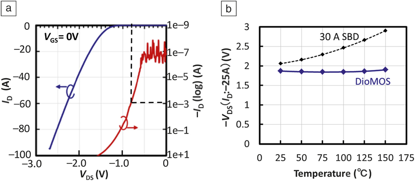
Diode operation is shown in Figure 5. The diode current flowing from source to drain and the I D–V DS characteristics with low PB are experimentally confirmed for –V DS(I D:1 mA) = 0.8 V, as shown in Figure 5a. I D = 1 mA is the same value that is used to define V th of the MOSFET operation. The temperature dependence of the conduction loss associated with the diode current measured as a function of –V DS(I D:–25 A), shown in Figure 5b, is small compared to the SiC Schottky barrier diodes and are similar to the MOSFET current since both pass through the same channel.
Electrical characteristics of diode current in the SiC diode-integrated metal oxide semiconductor field-effect transistor (DioMOS).Reference Ohoka, Horikawa, Kiyosawa, Sorada, Uchida, Kanzawa, Sawada, Ueda and Fujii16 (a) I D–V DS characteristics. (b) Temperature dependence of V DS at I D = 25 A. The dependence of a commercially available 30 A SiC Schottky barrier diode (SBD) is also shown. Small conduction loss during diode operation with (a) V DS(I D = 1 mA) = 0.8 V and (b) V DS(I D > 25A) is confirmed.
Applications of DioMOS for DC-DC converter
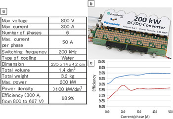
The SiC DioMOS was applied to a DC-DC converter for electric and hybrid vehicles, as shown in Figure 6a–c.Reference Kreutzer, Maerz and Nakata17 The designed SiC converter has six-interleaved-phases resulting in a hard-switching bidirectional DC-DC converter with a switching frequency of 200 kHz. The developed 200 kW/800 V full-SiC DC-DC converter includes DC-link capacitors, inductors, and gate drivers with a total volume of 1.4 dm3. The resultant power density was confirmed to be very large >100 kW/dm3, which is more than one order of magnitude larger than that of devices implemented with Si-IGBTs operating under the switching frequency of several kHz with very large capacitors and inductors.
DC-DC converter application using the SiC diode-integrated metal oxide semiconductor field-effect transistor (DioMOS).Reference Kreutzer, Maerz and Nakata17 (a) Key parameters. (b) Photograph of the 200 kW/800 V converter. (c) Efficiency of the converter (blue and red lines represent the conversions from 800 V to 667 V and from 650 V to 288 V, respectively, as a function of current. An efficiency as high as 98.9% is confirmed with the conversion from 800 V to 667 V. Six interleaved phases each with current/phase = 50 A results in a total current of 300 A. Note: DC, direct current.

The Baliga high frequency figure of merit of SiC is 50 times greater than Si. Conventional Si-IGBTs with a chip size of more than double that of SiC-MOSFETs also require additional interconnected diode chips, as opposed to the one chip solution provided by SiC-DioMOS. The bonded DioMOS chips are water-cooled with a 70°C temperature rise at full load. The efficiency of the converter in step-down mode is as high as 98.9% at full load.
Summary
A new technique for SiC epitaxial growth has been developed to grow ultrathin highly doped layers. This technique enables formation of layers with a thickness as thin as a few nm and doping concentrations of more than 1018cm–3. Application of this precisely controlled layer into the channel of a SiC MOSFET has successfully resulted in the realization of diode-integrated SiC DioMOS without any increase in the chip size. The DioMOS enables V th > 4.0 V for the MOSFET current and PB < 0.8 V for the diode current. The DioMOS described here exhibits BV > 1600 V, R ON = 20 mΩ, and specific R ON = 4.7 mΩcm2 with a low variation in device characteristics over a wide range of temperature. The unipolar conduction of the DioMOS promises fast switching without the R ON degradation. In terms of applications, a very small and light 200 kW/800 V DC-DC converter has been successfully demonstrated with a switching frequency of 200 kHz and a volume of 1.4 dm3. This converter works with an efficiency of 98.9% and power density of >100 kW/dm3. Such high frequency operations under high power densities would enable small power management systems for a wide field of future power electronics. These high-efficiency values represent a significant improvement over typical silicon device efficiencies of approximately 90% and would represent meaningful energy savings through a reduction in losses.
Acknowledgments
Masao Uchida, Yoshihiko Kanzawa, and all members of the development group for SiC-power devices at Panasonic are acknowledged for helpful discussions about the DioMOS. Otto Kreutzer is acknowledged for his effort to develop the converter for the DioMOS application.