I. INTRODUCTION
With the rapid development of wireless communication technology, the planar microwave filters with good frequency selectivity, compact size, and wide stopband have attracted much attention in recent years [Reference Hong and Lancaster1]. In [Reference Hsu, Chen and Chuang2], an efficient and practical design method for a dual-band bandpass filter (BPF) was presented to control and adjust the bandwidth and transmission to zero location. A compact dual-wideband BPF using an asymmetrical resonator was designed using three uniform microstrip lines of different lengths in [Reference Hsu, Chien and Tu3]. Authors in [Reference Fan, Zhan, Jin and Luo4] presented a novel wideband microstrip BPF based on a quadruple-mode ring resonator, which was created by introducing a stepped-impedance one-wavelength ring resonator into a stepped-impedance half-wavelength resonator. A compact dual-band BPF using stepped impedance resonators (SIRs) was introduced in [Reference Wei, Yue, Liao, Wang, Xu and Shi5]. Also, to improve the upper-stopband of the presented filter, tri-section folded SIRs were adopted. A four-pole dual-band BPF was designed with stub-loaded resonators and dual-feeding structure in [Reference Heng6]. A compact superconducting BPF using dual-mode loop resonator was developed and designed for wireless local area networks (WLAN) in [Reference Liu7] but its return loss is not appropriate. Also, they used shunt capacitive loading structure to enhance the self-capacitance and electrical length of the loop resonator. In this paper, an ultra-wideband BPF and a dual-band BPF are presented.
A) Main resonators
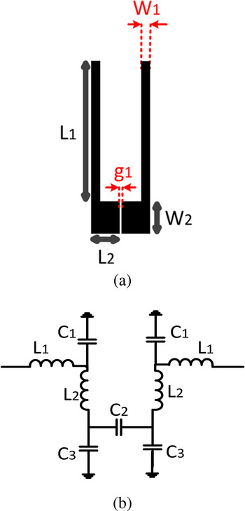
Figure 1(a) shows the layout of the resonator, composing of modified stepped impedances. The proposed resonator has good features for designing BPF. The equivalent LC circuit of the main resonator is shown in Fig. 1(b) so that L 2, L 3, and C 1 are inductances and capacitance of high-impedance lossless line. L 1 denotes the inductance of the transmission line and C 2 is the sum of equivalent capacitances of open-end and high-impedance lossless line. The values of these parameters can be extracted by using the methods discussed in [Reference Hong and Lancaster1] and they are summarized here.
(a). Layout of the proposed resonator; (b). L–C equivalent circuit.

The dimensions of the designed filter shown in Fig. 1(a) are as follows: L 1 = 7.01, W 1 = 0.44, L 2 = 1.42, W 2 = 1.6, and g 1 = 0.1 (all in millimeter).
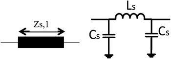
A high and low-impedance lossless line terminated at both ends with relatively low impedance lines can be presented by a Π-equivalent circuit, as shown in Fig. 2. The values of inductors and capacitors can be attained as:
 $${l_s} = \displaystyle{1 \over w} \times {z_s} \times \sin \left( {\displaystyle{{2\pi} \over {{\lambda _g}}}l} \right),$$
 $${c_s} = \displaystyle{1 \over w} \times \displaystyle{1 \over {{z_s}}} \times \tan \left( {\displaystyle{\pi \over {{\lambda _g}}}l} \right),$$
where Z s is the characteristic impedance of the line. l is the length of it, and λ g is the guided wavelength.
Layout and equivalent LC circuit of high and low-impedance lossless line.

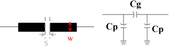
Formulas of open-end have investigated here. Its structure and equivalent circuit are shown in Fig. 3. The shunt and series capacitances C p and C g may be determined using [Reference Hong and Lancaster1] as follows:
 $$\eqalign{&{C_p} = 0.5{c_e}, \cr & {C_g} = 0.5{c_o} - 0.25{c_e},}$$
 $$\eqalign{\displaystyle&{{Co} \over W}\left( {\displaystyle{{pF} \over m}} \right) = {\left( {\displaystyle{{\varepsilon r} \over {9.6}}} \right)^{0.8}}{\left( {\displaystyle{s \over w}} \right)^{mo}}\exp \left( {{k_o}} \right), \cr &\displaystyle{{ce} \over w}\left( {\displaystyle{{pF} \over m}} \right) = 12{\left( {\displaystyle{{\varepsilon r} \over {9.6}}} \right)^{0.9}}{\left( {\displaystyle{s \over w}} \right)^{me}}\exp \left( {{k_e}} \right),}$$
 $$\eqalign{mo =& \displaystyle{w \over h}\left[ {\matrix{ {0.619} & {\log \left( {\displaystyle{w \over h}} \right) - 0.3853} \cr}} \right], \cr ko = & 4.26 - \matrix{ {1.453} & {\log \left( {\displaystyle{w \over h}} \right)} \cr} \quad \matrix{ {{\rm for}} & {0.1} \cr} \le \displaystyle{s \over w} \le 1.0,}$$
 $$\eqalign{me & = 0.8675, \cr ke &= 2.043{\left( {\displaystyle{w \over h}} \right)^{0.12}}\quad \matrix{ {{\rm for}} & {0.1} \cr} \le \displaystyle{s \over w} \le 0.3,}$$
 $$\eqalign{me & = \displaystyle{{1.565} \over {{{(w/h)}^{0.16}}}} - 1, \cr ke &= 1.97 - \displaystyle{{0.03} \over {w/h}}\quad \matrix{ {{\rm for}} & {0.3} \cr} \le \displaystyle{s \over w} \le 1.0.}$$
Layout and equivalent LC circuit of gap.

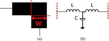
Formulas of bend have been summarized here. Right-angle bends of microstrips may be modeled by an equivalent T-network, as shown in Fig. 4. Gupta et al. [Reference Gupta, Garg, Bahl and Bhartis8] have given closed-form expressions for evaluation of capacitance and inductance as follows:
 $$\eqalign{& \displaystyle{c \over w}\left( {\displaystyle{{pf} \over m}} \right) = \cr & \quad \left\{{\matrix{ {\displaystyle{{\left( {14\varepsilon r + 12.5(w/h)} \right) - (1.83\varepsilon r - 2.25)} \over {\sqrt {w/h}}} + \displaystyle{{0.02\varepsilon r} \over {w/h}}} & {\displaystyle{w \over h}\;\langle \;1} \cr {\left( {9.5\varepsilon r + 1.25} \right)\displaystyle{w \over h} + 3.2\varepsilon r} & {\displaystyle{w \over h}\;\rangle 1,} \cr}} \right.}$$
 $$\displaystyle{l \over h}\left( {\displaystyle{{nh} \over m}} \right) = 100\left\{ {4\sqrt {\displaystyle{w \over h}} - 4.21} \right\}.$$
(a) Layout and (b) equivalent LC circuit of bend.

The calculated and optimized values for LC equivalent circuit are summarized in Table 1.
Calculated values for LC equivalent circuit. (Units: C, pF; L, nH).

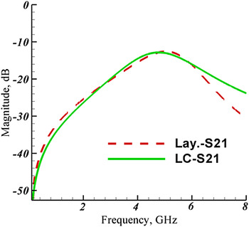
The electromagnetic momentum (EM) and equivalent circuit simulation results of the main resonator are in good agreement as shown in Fig. 5.
EM and circuit simulation results of main resonator.

The transfer function of two-part filter network is a mathematical description of network response characteristics, namely, a mathematical expression of S 21. So in this paper, transfer function of the main resonator (Fig. 1(b)) is calculated in equation (10). The transfer function of main resonator is achieved using Kirchhoff's voltage law (KVL) and Kirchhoff's current law (KCL) roles. Poles and transmissions zeros are obtained by the transfer function. The transfer function can be calculated with LC equivalent circuit (Fig. 1(b)) as follows:
 $$\displaystyle{{{v_o}} \over {{v_i}}} = \displaystyle{{ - ({c_1}rs)} \over {1 + s\left( \matrix{2{c_2}(r + {l_1}s)(1 + {c_3}{l_2}{s^2})(1 + (2{c_1} + {c_3}){l_2}{s^2}) \cr \quad + c_2^2 s{(r + {l_1}s)^2}(1 + {c_3}{l_2}{s^2})(1 + \left( {2{c_1} + {c_3}} \right){l_2}{s^2}) + \cr s(2{c_1}({l_2} + {c_3}l_2^2 {s^2} - {c_3}{(r + {l_1}s)^2}) \cr \quad + {c_3}( - {c_3}{(r + {l_1}s)^2} + {l_2}(2 + {c_3}{l_2}{s^2})))} \right)}}.$$
And S 21 is calculated with transfer function and it is defined as:
 $${S_{21}} = 20\log \left \vert {\displaystyle{{{v_o}} \over {{v_i}}}} \right \vert.$$
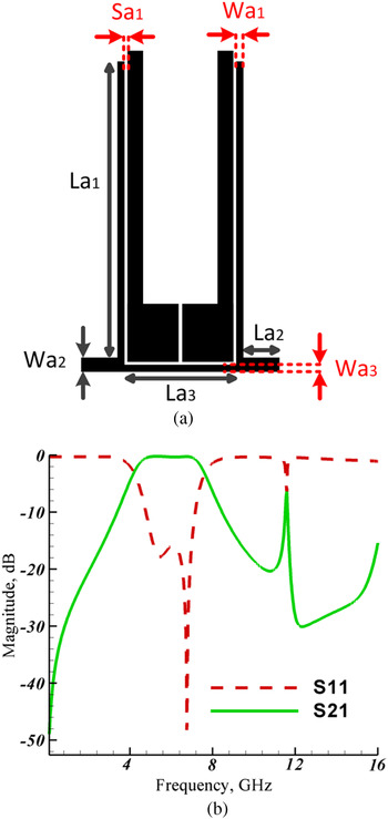
There is a transmission pole in equation (10) which is more important than other transmission poles. As shown in Fig. 5, the transmission pole of the main resonator is located at 4.4 GHz with attenuation level equal to 10 dB. To design wide band BPF, a new structure is added to the main resonator. The structure is made of some high impedance lossless line. Figure 6(a) shows layout of the proposed wide band BPF and frequency response of the filter is shown in Fig. 6(b). L 1 and L 2 are used for decreasing insertion loss as seen in Fig. 6(b). The dimensions of the designed filter, shown in Fig. 6(a) are as follows: L a1 = 7.59, W a1 = 0.2, L a2 = 1, W a2 = 0.4, L a3 = 3.1, W a3 = 0.2, S a1 = 0.08 (all in mm).
(a) The layout of the proposed wide BPF. (b) Frequency response of the proposed wide BPF.

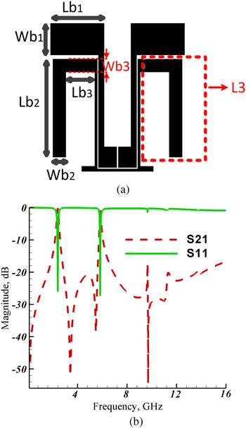
L 3 in Fig. 7(a) can generate some transmission zero so that one of the transmission zeroes is located in middle of pass band of the proposed BPF. We use the transmission zero for designing dual-band BPF, also from other transmission zeroes is utilized for increasing sharpness in transition band. L 3 consists of two high-and low-impedance lossless lines which can generate some capacitances and inductances (Fig. 2). The capacitances and inductances can generate several transmission zeros. Also the location of transmission zeroes can be changed by changing dimensions of L 3. We choose the dimension so that transmission zeros are located in the best places. Layout and frequency response of the proposed dual-band BPF are shown in Figs 7(a) and 7(b), respectively.
(a) The layout of the proposed dual-band BPF. (b) Frequency response of the proposed dual-band BPF.

The dimensions of the designed filter in Fig. 7(a) are as follows: L b1 = 4.12, W b1 = 2.42, L b2 = 7.5, W b2 = 1, L b3 = 2.2, W b3 = 1 (all in mm).
B) Simulation and measurement results
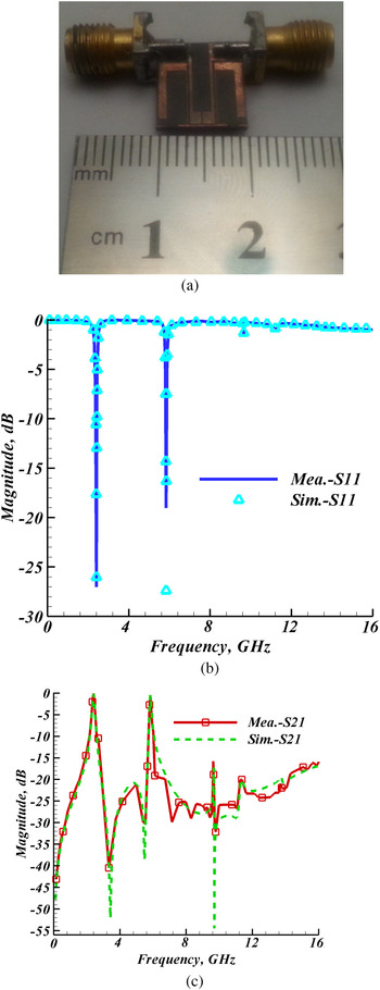
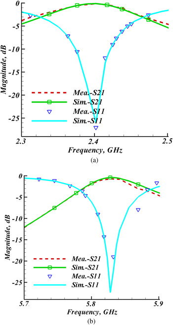
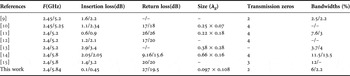
The photograph for the proposed filter is shown in Fig. 8(a). This filter is fabricated on a 31 mm thick RO5880 substrate with a relative dielectric constant 2.2 and loss tangent of 0.0009. From Figs 8(b) and 8(c), they are obvious that the realized filter has sharp transition band. This filter with passband is operated at 2.4/5.84 GHz. The designed dual-band BPF presents the insertion loss less than 0.1 and 0.4 dB. Also the return loss is 26 and 28 dB at 2.4 and 5.84, respectively. The overall size of the fabricated low-pass filter is about 8.9 × 9.9 mm2. The designed filter has been compared with other published filters in Table 2. Figures 9(a) and 9(b) show the enlarged form of Fig. 8(b) in bandpass bands to obtain a better insight about passband insertion loss, return loss, and bandwidths clearly.
(a) Photograph of the proposed filter. (b). Simulated and measured performance of the BPF (S 11). (c). Simulated and measured performance of the BPF (S 21).

Simulated and measured performance of the proposed BPF in the pass band (a) at 2.4 GHz. and (b) at 5.84 GHz.

Performance comparison among published filters and presented one.

II. CONCLUSION
In this paper, compact dual-band BPF based on novel L-shaped resonators is presented. Based on the principle, 2.4/5.84 GHz dual-band BPFs is implemented and measured, respectively. With the good frequency performances and compact size, the proposed filter is attractive to the WLAN applications.
 Yeganeh Pourasad was born in Karaj, Iran in 1987. She received her B.S. degree in Electronics Engineering in 2010 from Arak University, Arak, Iran. She is now a M.Sc. collegian in Electronic Engineering in Islamic Azad University, Science and Research Branch, Kermanshah, Iran. Her current research interests are RF/microwave circuit design.
 Gholamreza Karimi received his B.S., M.S., and Ph.D. degrees in Electrical Engineering from Iran University of Science and Technology, Tehran, Iran, in 1999, 2001, and 2006, respectively. Since 2007, he has been with the Electrical Department, Razi University, Kermanshah, Iran, where he is now an Associate Professor. His main research interests are low-power analog and digital IC design; RF/IC design; and modeling and simulation of RF/mixed signal IC. He is also interested in microwave devices and artificial intelligence systems