I. INTRODUCTION
The properties and application of c-axis ZnO has been widely researched and developed. However, its spontaneous piezoelectric polarization along the c-axis ZnO film can induce a large built-in electrostatic field and then separate the overlapping of electron and hole wave functions in the quantum well; this phenomenon, known as the quantum confined stark effect (QCSE), can lead to the deterioration of the internal quantum efficiency of light-emitting devices.
Reference Waltereit, Brandt, Trampert, Grahn, Menniger, Ramsteiner, Reiche and Ploog1,Reference Wetzel, Takeuchi, Amano and Akasaki2
Also, the special application of ZnO as a surface acoustic wave (SAW) device in liquids requires a film growing with the c-axis tilted away from the normal to the film surface.
Reference Wang and Lakin3,Reference Nistor, Ghica, Matei, Dinescub, Dinescub and Van Tendelooc4
Therefore, the growth of nonpolar ZnO films such as a-(
 $11\bar 20$
) or m-(
 $10\bar 10$
) plane has drawn attention as an alternative way for overcoming the QCSE problem and extending the application of SAW devices in liquids.
In general, the (0002) polar surface is the most preferable growth direction because of its low surface energy; the non polar a- or m-plane is the next preferable growth directions. Therefore, the preparation of nonpolar films was much more difficult than that of polar films. The difference between polar and nonpolar ZnO film is whether the c-axis is perpendicular or parallel to the surface of substrate. To realize the stable nonpolar film growth, a transition from polar to nonpolar growth is necessary. Researchers need to explore the conditions which may not only inhibit the polar film growth but also promote the non-polar crystal growth. Different film growth conditions Reference Cui, Du, Zhang, Zhu and Zhang5–Reference Liu, Babar Shahzad and Qi24 were adopted to grow nonpolar ZnO thin films on different substrates and to explore the related properties and microstructure characteristics. Such as the temperature and surface treatment, Reference Cui, Du, Zhang, Zhu and Zhang5–Reference Qi, Shahzad and Qi19 the deposition rate and the incidence angle, Reference Nistor, Ghica, Matei, Dinescub, Dinescub and Van Tendelooc4 the partial pressure, Reference Ma, Shang, Ma and Su20 the substrate plane Reference Tarsa, Heying, Wu, Fini, DenBaars and Speck21 and the elemental source flux ratio. Reference Zhang, Yao, Wang, Li, Shan, Zhang, Li, Zhang and Shen22–Reference Liu, Babar Shahzad and Qi24 Temperature is one of the most important growth parameters because of its significant influence on interfacial microstructure, surface morphology, dislocation generation, and photoluminescence properties. Up to now, many nonpolar ZnO films have been successfully prepared at 200–900 K. For the alternation of the preferred growth surface from polar to nonpolar, some scientists insisted that high temperature can suppress the formation of polar ZnO films, Reference Chen, Pan, Ding, Zhang, Chen, Dai, Huang and Ye6,Reference Elanchezhiyan, Bae, Lee, Shin and Kim11 whereas others stated that nonpolar films can be obtained under nonequilibrium conditions, such as low temperature (473 K) or high deposition rate. Reference Lu, Ye, Huang, Wang and Zhao12 Though the growth temperature is closely related with the other conditions, such as deposition methods, substrate, doping element, et al., the low temperatures treatment can effectively reduce the disorder state, surface roughness, and point defects in ZnO film in any circumstances. Therefore, some scientists had focused on developing methods to obtain high-quality nonpolar ZnO films at low temperatures. However, despite the considerable efforts exerted to grow nonpolar ZnO films, the growth mechanism, microstructure characterization, and defect formation of such films remain poorly understood when compared with those of c-axis films. Therefore, the effect of temperature on nonpolar ZnO film qualities, as well as the film growth mechanism and microstructure evolution, must be elucidated to promote the preparation and widen the applications of these films.
In consideration of the limited experimental work on this aspect, theoretical studies are quite needed to provide unique insights into the growth mechanisms and structural evolution of nonpolar thin films. Compared with bulk materials, film growth is much more complicated because it involves atomic bond breaking and reforming on the substrate interface and growth surface. Reactive force field (ReaxFF) methods, Reference van Duin, Dasgupta, Lorant and Goddard25–Reference Zhang, Cagin, van Duin, Goddard, Qi and Hector27 which can simulate the breaking and reforming phenomena of bonds during a dynamic evolution process, and can describe chemical and physical properties accurately, were quite suitable for studying the film growth processes. Liu et al. had previously studied the effect of the Zn/O ratio (substrate temperature) on a- (c-) oriented film growth. Reference Liu, Babar Shahzad and Qi24,Reference Liu, Liu, Li and Qi28 It was found that the c-axis thin film grew with an island mechanism, and two orientations presented on the deposited atomic plane. Reference Liu, Babar Shahzad and Qi24 The initial formation of a-axis film can be described as a process of individual atoms → atomic clusters → atomic chains → localized films. Reference Liu, Liu, Li and Qi28 Based on previous study, further exploration of the layer development and the interfacial microstructure evolution under different temperature regime is necessary. The difference of film growth condition and mechanism between c- and a-axis is also needed to be elucidated.
ReaxFF method was adopted in the present work to study the effect of temperature (350–950 K) on microstructure and growth mechanisms of a-axis ZnO films on the perfect substrate. The film nucleation and growth mechanisms at low temperature and the corresponding film growth mode were emphasized to fill the gaps in previous studies. The film deposition model was shown in Sec. II. The influence of different temperatures on film quality was comprehensively discussed in Sec. III in view of average energy, crystallize quality, layer coverage, and ionic injecting and sputtering behaviors. For the film grown at the optimal temperature, the corresponding film growth condition, layer growth mechanism, and defect configurations were further discussed. The summary and conclusions were given in Sec. IV.
II. CALCULATION DETAILS
A. Model and method
To study the growth of a-axis ZnO films, the axis of the deposition model was oriented with a-[
 $11\bar 20$
], b-[
 $10\bar 10$
], and c-[0001] on the basis of the lattice parameters a
0 = 3.25 Å,
 $b_0 = {{\sqrt 3 } \over 2}a_0$
= 2.81 Å, and c
0 = 5.21 Å [Figs. 1(a) and 1(b)]. Here the (
 $11\bar 20$
) plane was set as the depositing surface. The substrate adopted the NVE ensemble, where N is the number of particles, V is the system volume, and E is the total energy. The bottom [marked by orange balls in Fig. 1(c)] was fixed to stabilize the deposition model, and the atoms in the bottom region moved as a whole under external forces. Considering the nature of virtual experiments, we applied another temperature rescaling factor to the yellow O and light blue Zn marked region in Fig. 1(c) to maintain a constant substrate temperature. This temperature rescaling application can modify velocities to affect thermostat but not perform time integration. The above setup can (i) reflect the temperature influence on the substrate; (ii) define a stable and natural deposition condition for the film growth [Fig. 1(c)]. The size of the substrate was 8a
0 × 16b
0 × 15c
0 with a total of 9600 atoms, 16 atomic layers. The deposition atoms (960 O and 960 Zn, 4 atomic layers) were randomly emitted at the distance between 10 and 14 Å above the substrate surface every 6000 time steps (t
0 = 0.25 × 10⁻³ ps) with a velocity of 2.5 m/s [Fig. 1(c)].
Redefined ZnO crystal structure in the direction of [
 $11\bar 20$
], [
 $10\bar 10$
], and [0001]. (a) Vertical stacking along c-[0001]. (b) Vertical stacking along a-[
 $11\bar 20$
]. (c) Profile view of the a-plane ZnO deposition model.

The Zn–O parameters developed by Raymand et al. within ReaxFF frame Reference Raymand, van Duin, Baudin and Hermansson29 was adopted in the present work. It can clearly describe all of the Zn and O bonding and physical states (bulk crystal, molecular, and cluster), and can successfully emphasize on obtaining a good surface description.
The simulation of ZnO film growth included three steps: optimization before deposition (100,000t 0, 25 ps), deposition (5,760,000t 0, 1440 ps), and optimization after deposition (500,000t 0, 125 ps). The simulation was conducted on Lammps (Large-scale Atomic/Molecular Massively Parallel Simulator) Reference Plimpton30 platform.
III. RESULTS AND DISCUSSION
The effect of temperature on a-axis film quality was considered from the film stability, layer coverage, crystallization, point defect by calculating the total energy, atomic density, radial distribution function (RDF), and the numbers of injected and sputtered species of the newly formed ZnO films. Based on above consideration, we determine the optimized film growth condition. Further, the comparison of c and a film growth condition, the snapshots of instant Zn2+ and O2− deposition, layer stacking, and defect configuration under the optimal condition were discussed to explore the nonpolar film nucleation and growth mechanism, as well as the defect formation mode.
A. Temperature effect on the film stability
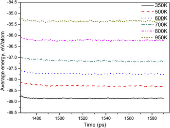
Firstly the average energy variation as a function of time at the optimization stage after deposition was given to evaluate the system stability at different substrate temperatures (Fig. 2). All of the energies finally drop to a dynamical equilibrium value, implying that the deposited atoms have grown into a stable film in the corresponding condition. The average energy is reasonably increased when the temperature changes from 350 K to 900 K (Fig. 2), which implies that the film grown at high temperatures is less stable than those grown at low temperatures.
Variation of average atomic energy as a function of time at different substrate temperatures during the last optimization stage.

B. Temperature effect on the film coverage and crystallization
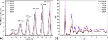
To evaluate the film coverage, the atomic number on each new layer was calculated and the result was shown in Fig. 3(a) together with the top 16th layer of the substrate. The newly formed ZnO crystal film contains thickness of two ZnO perfect crystals, i.e., 4 perfect atomic Zn–O layers. After full relaxation, the film layers adjacent to the substrate were clearly arranged, while the layers close to the surface were mixed with atoms. Here we took the average layer distance of 17th–19th as a standard to extract the film layers of 17th–20th, and all the other atoms were taken as 21st layer. Since most atoms located in the central region between two layer boundaries, the present extract method will not obviously affect the following result of atomic number, layer distance, and the total injecting and sputtering number. The interlayer spacing slightly increases when the substrate temperature changes from 350 K to 950 K. For all of the films grown at different substrate temperature, the 17th layer possesses the similar density comparing with that of 16th layer. The atomic density of other layers decreases when they are more close to the surface because of the defects and morphology changes induced by the atomic deposition and migration. Higher atomic density might mean better layer coverage and less film roughness. Take 17th–19th layers as the objective films, we can speculate that the films grown at 500–600 K possess better qualities than those grown at other temperatures [Fig. 3(a)]. The 20th–21st layers were not considered because of the excessive defects induced by the special surface morphology.
(a) Atom number of each film layer and (b) the total RDF of ZnO film at different temperatures.

Figure 3(b) presented the total RDF of the newly formed ZnO films at different temperatures. Obviously, the film grown at 500 K possesses the highest peak, followed by the films grown at 600, 700, and 350 K. The film grown at 800–950 K presents poor crystallization state. Therefore, the film grown at 500 K possesses better crystallizations than those grown at other temperatures. Some experimental studies Reference Elanchezhiyan, Bae, Lee, Shin and Kim11–Reference Dai, Han, Wu, Yu, Xiang, He, Gao, Chen, Xiao and Peng16 had also showed that the optimal temperature of a-plane ZnO films is approximately 500 K. Further investigation of the RDF of Zn–Zn and O–O relations showed minimal variations with temperature. This result implies that temperature exerts only a slight effect on the interaction between the same atoms.
C. Temperature effect on the injecting and sputtering phenomena
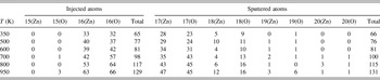
The ionic injecting and sputtering behaviors are important because they can promote the formation of point defects, which can greatly influence the film coverage, surface, and interfacial morphologies. From Table I, we can find that the injecting and sputtering phenomenon mainly occurs at the interface (16th/17th layers). The number of injecting and sputtering atoms increases slowly when the temperature changes from 350 to 600 K. But when the temperature exceeds 600 K, the injecting and sputtering atom number increases rapidly. In general, a large number of injected and sputtered atoms are related to a severe nonequilibrium growth of ZnO films, and possible emergence of the point defects such as the interstices or vacancies. It can be seen that the injecting and sputtering behaviors can be better controlled at low temperatures (500–600 K) with less migration of atoms and point defects than those happen at high temperatures (Table I).
Number of injected and sputtered atoms on different layers at different substrate temperatures.

D. Growth conditions and mechanisms
A comprehensive analysis of film stability, layer coverage, crystallization state, and sputtering/injecting behaviors revealed that the films grown at approximately 500–600 K possessed better qualities than those grown at other temperatures. Therefore, the film growth conditions, mechanisms and microstructure characteristics were further studied under the optimized temperature condition.
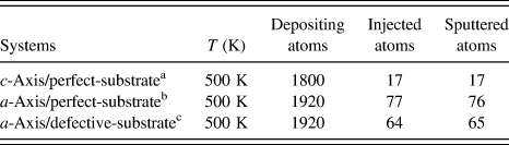
Table II showed the comparison of the injected and sputtered atoms in different film growth systems at same substrate temperature. The number of injected/sputtered atoms in the condition of the a-axis/perfect-substrate is a little higher than that of the a-axis/defective-substrate condition, and is much higher than that of c-axis/perfect-substrate condition. That may indicate a more nonequilibrate condition for a-axis film growth than that of c-axis film formation. From the comparison of a- and c-axis film growth, we can reasonably conclude that the injecting and sputtering behaviors can effectively induces the nonequilibrium condition, which may alter the preferable film orientation from c-axis to a-axis. The further comparison of a-axis film growth with and without preexisting defects indicates that another driving force of nonequilibrium condition can be provided by the defect, which may effectively relaxes the injecting and sputtering burden to keep the nonequilibrium state, and thus lower the injected and sputtered atoms, reduce the point defects in the film. Therefore, besides the nonpolar substrate, a nonequilibrium growth condition and a small amount of defects may be two other key factors which can promote the transition of preferable film growth direction from c to a or m. To achieve a nonequilibrium condition, extremely thin nonpolar seed layer (strong interfacial interaction), short growth period, high depositing rate, low substrate temperature and preset defects may be the potential factors needed to be considered. Some of above mentioned points had been supposed to be the dominant factors which can effectively inhibit the c-axis growth and promote the growth of the a-axis film. Reference Lu, Ye, Huang, Wang and Zhao12,Reference Qi, Shahzad and Qi19
Number of injected and sputtered atoms in different film growth systems and same substrate temperature.

a Ref. Reference Liu, Liu, Li and Qi28.
b Present work.
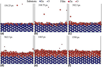
Snapshots of instant film growth (Fig. 4) at 600 K were captured to show detailed microstructure evolutions at different time-steps. All of the substrates maintained perfect stacking during deposition process [Figs. 4(a)–4(e)]. The presence of red (blue) atoms in the substrate (new film) indicates the injecting (sputtering) behavior through the interface in Figs. 4(a)–4(c). The bonding of Zn–O, O–Zn–O, Zn–O–Zn, and island growth mode can be observed in Figs. 4(b)–4(d). Atom deposition was completed at 1465 ps [Fig. 4(e)], and the final film became more ordered after another 125 ps relaxation [Fig. 4(f)].
Instant atomic snapshots of a-axis ZnO film during growth process at 600 K. The atoms of substrate (new film) are marked by dark blue (red) balls. Zn and O atoms are represented by large and small balls, respectively.

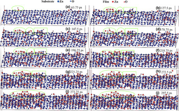
Snapshots of surface morphology evolution were captured (Fig. 5) to reveal the film growth mechanism. In the bulk wurtzite ZnO structure, Zn2+ (O2−) is bonded to four neighboring O2− (Zn2+) to form the tetrahedral configuration, and only Zn–O atomic chains can be observed on the substrate surface [16th layer, Fig. 5(a)]. Based on the nucleation and formation of 1st layer (individual atoms → atomic clusters → atomic chains → continuous films), Reference Liu, Liu, Li and Qi28 we further observed the initiation and growth of the 2nd layer in the present work. In the film initiation stage, most Zn atoms adhere to formerly existing O atoms, or vice-versa, and then act as potential nucleation sites for the following depositing atoms. The regions marked by ovals, circles, and squares were given as examples to study the growth of the 1st film layer and the following layers. New layers are initiated either from the deposited atoms (oval- and circle-marked sites) or the sputtered atoms (square-marked sites). Then, the initial single Zn–O bonding extends to clusters, chains, and local films with the addition of more depositing atoms [Figs. 5(b)–5(g)]. Joining of the depositing atoms to the newly formed films disrupts the equilibrium state and induces the breakage and reconstruction of the bonding [Fig. 5(h)]. As a result, some atoms in the new film are unstably jointed to other atoms with some dangling bonds remained, and some atoms are instantly extruded along the direction out of the new film. The atoms out of the preexisted film can effectively become new nucleation sites for the next layer [Figs. 5(i) and 5(j)] and then induce the growth of a new layer.
Interfacial atomic snapshots of the initial film growth on the top substrate layer at different deposition times. Substrate (film) atoms are marked by blue (red) balls. Zn (O) atoms are represented by large (small) balls.

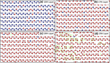
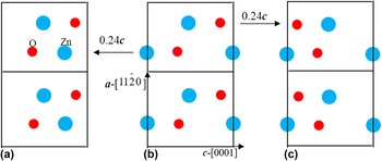
To study the film stacking mode and the defect formation in detail, the newly formed 17th–19th atomic layers were demonstrated in Fig. 6 together with the top substrate 16th layer. First, the atoms in the interfacial 16th–17th layers [Figs. 6(a) and 6(b)] are distributed in good order, even though the sputtering and injecting behaviors are fairly frequent. Second, the new film grows mainly in an A/B/A/B stacking order as a perfect ZnO crystal. The least defects are observed on the 17th–18th layers [Figs. 6(b) and 6(c)], and complicated surface morphology is found on the 20th–21st layers. Thus, the defects on the 19th [Fig. 6(d)] layer may deserve more attention than those on the other layers. Point defects such as the VZn and VO vacancies and the IO interstitial can be found easily on the 19th layer. These point defects cause the surrounding atoms to reconstruct into localized ordered configurations such as Zn2–O2 and Zn3–O3, as marked respectively by rhombi and rectangles in Fig. 6(d). A local anti-phase domain [marked by dashed ovals in Fig. 6(d)] also appears in the seriously distorted region. Among all the configurations, Zn2–O2 was the most frequently observed one, and had been found in other experimental works. Reference Tsuji and Hirohashi31 Combined with the limited studies of defects on nonpolar ZnO films, Reference Vennegues, Chauveau, Korytov, Deparis, Zuniga-perez and Morhain32–Reference Yadav, Sreenivas, Gupta, Singh and Katiyar34 the present Zn2–O2 might be related to the climbing of O or Zn in a plane with g c (Fig. 7) or g c+a mode. In consideration of the significant influence of defects (point/dislocation/stacking fault) on the optical and electrical properties of ZnO, further studies on the corresponding stability, formation, and control mechanism are still needed.
Layered snapshots of a-plane new film obtained at 600 K. Large and small blue (red) balls represent Zn and O atoms of the substrate (new film), respectively. The circles, triangles, and squares denote the VZn and VO vacancies and the IO interstitial, respectively. The rhombi, rectangles, and ovals denote the fault configuration of Zn2–O2, Zn3–O3, and anti-phase domain, respectively.

Formation schematic of the Zn2–O2 configuration.

IV. CONCLUSIONS
We investigated the effect of temperature (350–950 K) on the growth of a-axis ZnO films at a deposition rate of 2.5 m/s using the ReaxFF-based molecular dynamics method. The following conclusions can be drawn:
-
(1) An analysis of total energy, crystallize quality, injecting and sputtering phenomena, and layer coverage showed that the films grown at approximately 500–600 K possessed better qualities than those grown at other temperatures.
-
(2) Besides the nonpolar thin substrate, the nonequilibrium condition induced by low temperature, high depositing rate, preexisting defect, short growth period, strong interfacial interaction may potentially alter the preferred growth surface from polar to nonpolar.
-
(3) Snapshots of interface morphology evolution reveal that the mechanism underlying film nucleation and formation is as follows. First, with the addition of more depositing atoms, an initial single Zn–O bonding grows into atomic clusters, chains, and then a localized film. Then the addition of more atoms leads to the breakage and reconstruction of the localized film and induce some partially bonded or extruded atoms out of the film plane. Last, further adherence of depositing atoms to these unstable and extruded atoms induces the initiation and growth of a new layer.
-
(4) Multiple point defects and distortion-induced fault configurations were observed. The point defects are induced by the combined action of random injecting and sputtering phenomena on the surface and the island growth mode; meanwhile, the reconstructed configuration of Zn2–O2 might be related to the climbing of dislocation g c or g c+a . Further work is still needed to elucidate the formation mechanisms and related influence on thin film properties.
ACKNOWLEDGMENTS
This research was financially supported by the Fundamental Research Funds for the Central Universities (No. L1502038) and the National Natural Science Foundation of China (No. 51172040 and 51371177). This work was conducted in Shenyang Supercomputer Center at the Institute of Metals Research.