Purposeful review of credible articles and case-driven comparison
Microwave absorbers are crucial for reducing electromagnetic (EM) interference and radar cross-sections in civil and military applications, also for camouflage. They utilize coatings with specific permittivity or permeability to dissipate energy, emphasizing broad absorption bands [Reference Zaker and Sadeghzadeh1]. Based on the article’s title and key objectives, we purposefully review advancements in the absorption bandwidth of EM absorbers. This review utilizes highly cited and reputable articles and focuses on achieving perfect absorption by addressing both co- and cross-polarization components. To facilitate fair comparison and analysis of absorption-bandwidth increase reasons, Table 1 demonstrates these reviews in four categories, as follows:
- Primary and basic category (Dallenbach layers [Reference Dallenbach and Kleinsteuber2] and Salisbury screens [Reference Salisbury3]): Dallenbach absorbers use a λ/4 substrate on a conducting plane, while Salisbury screens incorporate a 376.7 Ω/square resistive layer, improving impedance matching but with narrow bandwidth.
- First category (resistive surface and capacitive loading): To make absorption-bandwidth progress, multiscreen and capacitive loading are employed [Reference Knott and Lunden4]. Circuit analogue absorbers use resistive patches for tunable frequency bands [Reference Costa, Monorchio and Manara5–Reference Kazemzadeh7]. The professional latest absorber, with multiple resistive/capacitive sheets and over 177% bandwidth, is detailed in [Reference Kong, Zhang, Pang, Fu, Zhao and Shen8].
- Second category (combining lumped resistors in 2D absorbers): The use of 2D frequency selective surfaces allows for the integration of metal patterns and surface-mount resistors, adding design flexibility [Reference Shang, Shen and Xiao9–Reference Zhang, Jin and Shen11]. It is challenging to increase the absorption bandwidths in this category solely by exploiting the fundamental modes. This problem has been solved in [Reference Zhang, Jin and Shen11] by using multimode resistor-embedded metallic strips.
- Third category (loading lossy resistors in 3D absorbers): Recent 3D absorbers focusing on multi-cavity designs enhance broadband absorption without thickness increase. Notable examples include microstrip [Reference Rashid, Shen and Aditya12] and strip-line [Reference Omar and Shen13] arrays that utilize lossy resistors for wideband absorption. Improved wideband absorbers leverage nonoverlapping modes of two lossy resonators [Reference Luo, Yu, Yu, Zhang and Shen15] and spoof surface plasmon polaritons [Reference Li, Hu, Yang and Yi16]. Current designs often involve multiple resistive elements, complicating their realization. A new method [Reference Zhu, Li, Zhang, Huang, Li and Zhu14] allows accurate parameter determination with single lossy resistor, reaching over 137% absorption bandwidth.
Comparison of absorbers in development based on four categories (Cat.: category, Rs: resistive surface, Nr: number of resistors, Th.: thickness, FBW: fractional BW)

This extensive review of the evolution of absorbers and Table 1 demonstrate that [Reference Zaker and Sadeghzadeh1, Reference Kong, Zhang, Pang, Fu, Zhao and Shen8, Reference Zhu, Li, Zhang, Huang, Li and Zhu14, Reference Tretyakov17, Reference Qin, Sun, Wang, Guan and Chen18]:
(1) Without resistors or lossy surfaces and substrates, only narrowband absorption can occur resonantly, and coupling multiple resonators increases design and fabrication complexity, leading to response instability.
(2) To broaden the absorption bandwidth, either increasing the number of resistors or increasing the thickness is necessary. This principle also applies to absorbers with resistive surfaces.
(3) Based on reflection graphs in reputable articles, complete elimination of both co- and cross-polarized reflection components is crucial for perfect absorption. This concept has been over-looked in some papers like [Reference Khanna and Awasthi19 and Reference Amugothu and Damera20], leading to erroneous conclusions about the absorption mechanism and suggesting polarization conversion (i.e. cross-polarizer), rather than perfect absorption. Addressing this problem and resolving it, along with the correct method of software simulation and the necessary computation data, are the main objectives of this corrigendum.
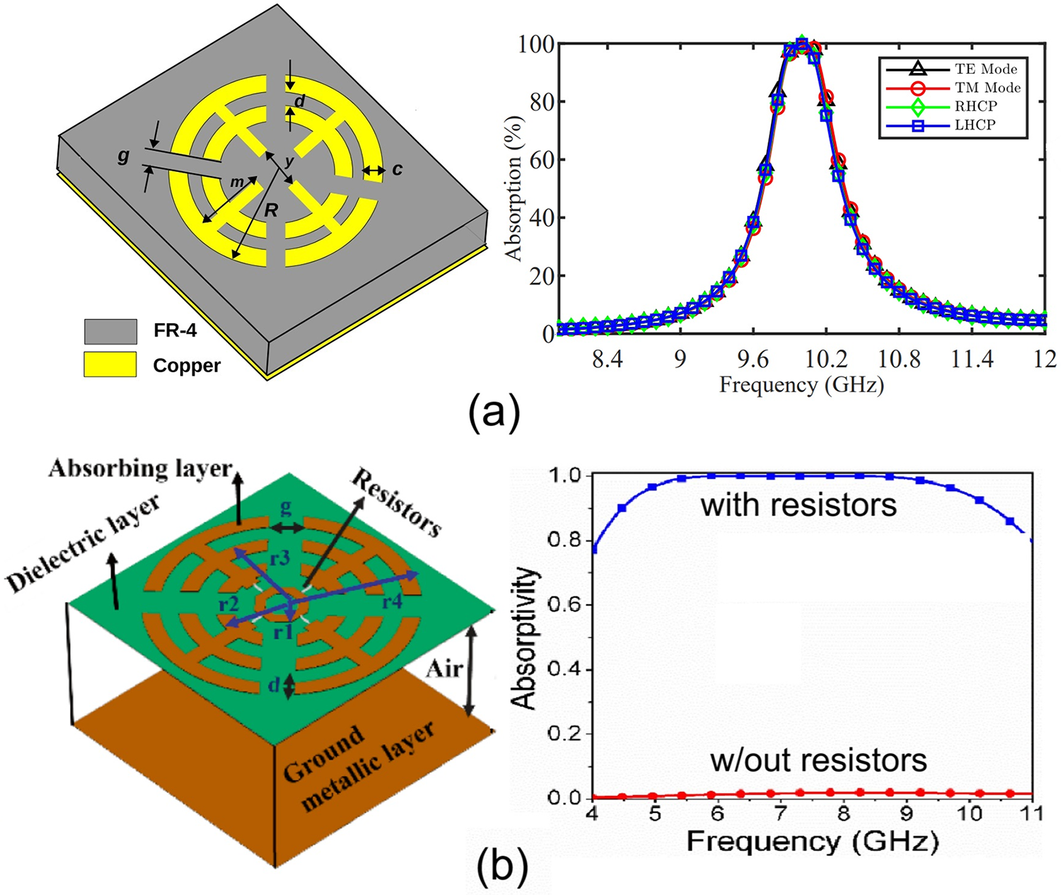
As the second targeted study, two valuable papers [Reference Choukri, Takhedmit, El Mrabet, Aznabet and Cirio21, Reference Rani, Bohre and Bhattacharya22] with accurate simulations and reliable results are compared, addressing the presence or absence of lossy resistors in the absorber. Figure 1 shows the structure of the similar metasurface-like absorbers proposed in [Reference Choukri, Takhedmit, El Mrabet, Aznabet and Cirio21] and [Reference Rani, Bohre and Bhattacharya22], respectively without and with resistors, and their absorption diagrams. Both absorbers have a similar structure, with the second design differing by embedding four lossy resistors on the metasurface. The first design’s absorption shows a narrow-band resonant behavior around 10 GHz (Fig. 1(a)). In contrast, the second design with similar structure achieves a notably wider absorption bandwidth due to the resistors. Figure 1(b) also shows a comparison in absorption with and without the resistors [Reference Rani, Bohre and Bhattacharya22]. This study proves that multiple resistors are essential to move beyond resonant behavior and achieve a wide bandwidth. Besides, the four orthogonal resistors enable damping in all directions, reducing all reflection components (co- and cross-polarizations). Damping only co-polarized component leads to a cross-polarizer, not a complete absorber.
(a) Meta-like resonant absorber without resistors [Reference Choukri, Takhedmit, El Mrabet, Aznabet and Cirio21] and (b) similar absorber with resistors [Reference Rani, Bohre and Bhattacharya22].

Absorption-calculation and HFSS simulation requirements
We assess an absorber by placing its surface in the x–y plane and directing waves along the z-axis. For incident x-polarized light, we evaluate four components: transmission through the absorber ( ${T_{xx}}\,$and
 ${T_{yx}}$), and reflection from it (
 ${R_{xx}}$and
 ${R_{yx}}$). Usually, the transmission is nullified due to the presence of a ground plane at the bottom surface of the substrate, and hence, the Absorption parameter is determined only from reflection components
 ${R_{xx}}\,$and
 ${R_{yx}}$, as:
 $Absorption = 1 - \left( {{{\left| {{R_{xx}}} \right|}^2} + {{\left| {{R_{yx}}} \right|}^2}} \right)$; when
 ${T_{xx}}$ =
 ${T_{yx}}$ = 0. (1)
To achieve Absorption equal to 1, both  ${R_{xx}}$ and
 ${R_{yx}}\,$must be zero. Accurate simulation of both reflected components, particularly
 ${R_{yx}}$, is essential. This was not done correctly in [Reference Khanna and Awasthi19 and Reference Amugothu and Damera20].
If the absorber structure is not symmetrical from the perspective of the x- and y-axes, proper pairing of reflection parameters ( ${R_{xx}}$/
 ${R_{yx}}$ for x-directed incidence,
 ${R_{yy}}$/
 ${R_{xy}}$ for y-incidence) is critical for Absorption calculation in Eq. (1). Using the incorrect pairing can give erroneous results; this is demonstrated in [Reference Amugothu and Damera20].
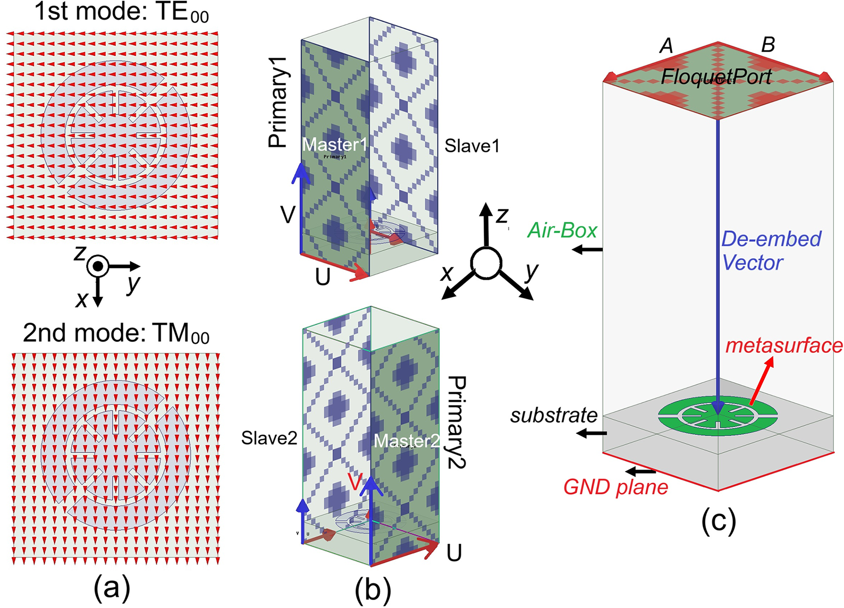
Ansoft/Ansys-HFSS software employs Floquet port for simulating radiation on cell surfaces. For simulating a uniform plane wave on the unit cell, the Floquet port uses two fundamental modes, TE00 and TM00. The related field orientations are shown in Fig. 2(a): in TE00, the field aligns with the negative y-axis, and in TM00, it aligns with the x-axis. According to these field directions’ definitions, and for a comprehensive guide on how to select the appropriate pairs for calculating Absorption in the HFSS software’s report section, Table 2 is provided for the first and second mode incidents. A key point in simulations that has been overlooked in numerous papers is that after designing the cell and defining the Floquet port in its Airbox, the directions of the first and second modes must be identified. Next, according to this table, the correct pair of S parameters must be selected for the Absorption calculation in Eq. (1).
(a) TE00-TM00 field directions, (b) definition of Primary1-Secondary1, Primary2-Secondary2 boundaries and their U/V vectors, (c) Floquet port with A and B vectors, and de-embed vector.

Correct reflected S parameter pairs for each incident mode to be used in Eq. (1) (e.g. y-axis inc.: y-axis directed incident)

In the following, to accurately simulate a cell in a 2D periodic array, proper boundary conditions must be defined on the Airbox. Older HFSS versions used “Master-Slave” conditions, now replaced by “Primary-Secondary.” Figure 2(b) shows the correct definition and U/V vector directions. To ensure accurate simulation of symmetric and asymmetric cells in an array, follow these guidelines [23]:
(1) U vectors for Master1-Slave1 pair must be parallel; this must also hold true for the 2nd pair.
(2) In asymmetric cells, Master2’s U vector starts at the end of Master1’s U vector.
(3) V vectors on all four Airbox sides must point inward.
(4) Define Floquet-port lattice-vectors: “A” from Master1 to Slave1 or vice versa, “B” perpendicular to “A”, both starting from the same point (see Fig. 2(c)).
(5) Use the de-embedded distance parameter, from the port to the cell’s upper surface (Fig. 2(c)), to precisely calculate wave phase.
Re-evaluation and re-simulation of [Reference Khanna and Awasthi19, Reference Amugothu and Damera20] and result correction
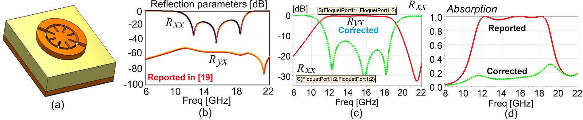
In this section, we focus on re-simulating the two designs presented in papers [Reference Khanna and Awasthi19] and [Reference Amugothu and Damera20], utilizing the simulation principles outlined earlier. Validated results are provided, along with comparisons to the original findings to highlight discrepancies. The first design referenced in [Reference Khanna and Awasthi19] is illustrated in Fig. 3(a), with simulation images shown in Fig. 2, generated using HFSS software, version 2023. As seen in Fig. 3(b), the co-polarized reflection ( ${R_{xx}}$) features a wide bandwidth with three resonances, while the cross-polarized reflection coefficient (
 ${R_{yx}}$) reveals a remarkably low value throughout the bandwidth, attributed to errors in simulation and reporting. Our simulation results in Fig. 3(c) confirm the same
 ${R_{xx}}$qualities. Interestingly,
 ${R_{yx}}$approaches 0 dB, indicating minimal damping of the cross-polarized component. This suggests that although the co-polarized component experiences damping, the orthogonal component reflects toward the port with negligible losses, allowing this design to function as a reflection polarizer (from co-polarized-incident into the cross-reflected component) rather than a perfect absorber. As seen in this figure, note that the S parameters and the selected pair for calculating Absorption are chosen according to Table 2. Furthermore, Fig. 3(d) proves that the corrected Absorption is significantly lower than previously reported, indicating weak single-resonance absorption around 19 GHz.
(a) Design proposed in [Reference Khanna and Awasthi19], (b) reflection parameters reported in [Reference Khanna and Awasthi19], (c) corrected reflection parameters, and (d) Absorption parameters, reported in [Reference Khanna and Awasthi19] compared to Eq. (1) with corrected data.

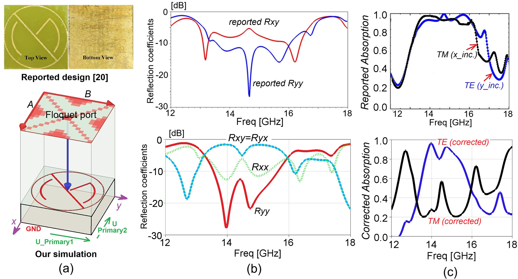
The second article, which seemingly contains an error in the Absorption calculation, is reference [Reference Amugothu and Damera20]. The photograph of the related prototype is presented in Fig. 4(a). This figure also shows our HFSS-based simulation setup, defined based on principles outlined in the previous section. In this structure, there is no symmetry relating parallel incidence along the x- and y-axes. Consequently, careful selection of the appropriate pairs of reflection components for calculating Absorption in Eq. (1) according to Table 2 is essential. The image above in Fig. 4(b) presents the reflection components for the design reported in [Reference Amugothu and Damera20]. Accordingly, the relatively high ranges of  ${R_{yy}}$and
 ${R_{xy}}$, particularly the cross-component (
 ${R_{xy}}$), suggest that an Absorption close to 100% (or 1) should not be achieved in the range of 13–16 GHz. However, the top image in Fig. 4(c) contradicts this, indicating a likely error in the graph presented in that reference. To clarify the miscalculation, we re-simulated all reflection components for both incidences, as shown in the lower image of Fig. 4(b). Notably, the optimal parameters provided in [Reference Amugothu and Damera20] were used in this simulation. A comparison with the reported data in [Reference Amugothu and Damera20] reveals several potential errors:
(1) The input port matching graphs,
 ${R_{xx}}\,$and
${R_{yy}}$are significantly different, primarily due to the physical asymmetry in the proposed cell. The input matching from the x-direction perspective is weak, indicating a relatively high
${R_{xx}}$, which implies a lack of absorption in that component. Beyond this incidence angle, no absorption occurs, as demonstrated in the lower image of Fig. 4(c) for TM incidence. Only two relative absorption peaks at 16.5 and 17.5 GHz are visible.
(2) A comparison of the graphs in Fig. 4(b), top and bottom ones, suggests that the
${R_{yy}}\,$graph is correctly presented, but the main error lies in the
${R_{xy}}$graph, where a lower value was mistakenly reported, leading to an overestimation of Absorption. Our simulation results indicate that, erroneously, the data for
${R_{xx}}\,$were reported instead of
${R_{xy\,}}$in [Reference Amugothu and Damera20]. Therefore, the Absorption graph was incorrectly calculated and presented.(3) Based on the corrected data, the Absorption graphs for TE and TM incidents are shown in Fig. 4(c), which reveal significantly lower values than those reported in [Reference Amugothu and Damera20]. The conclusion is that the presented design is not a perfect absorber and may instead be described as a relatively good polarizer from the co- into the cross-component in reflection mode.


(a) Fabricated prototype reported in [Reference Amugothu and Damera20] and its software setup for re-simulation, (b) reflection coefficients, reported in [Reference Amugothu and Damera20] and corrected data, and (c) Absorption graphs for TE and TM incidents, reported in [Reference Amugothu and Damera20] and corrected ones, using Eq. (1).

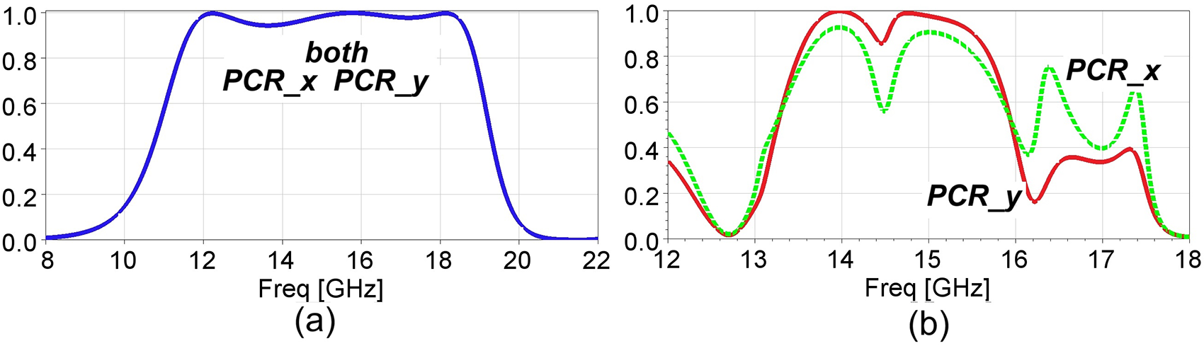
To prove that the designs presented in [Reference Khanna and Awasthi19] and [Reference Amugothu and Damera20] function as cross-polarizers rather than absorbers, the polarization conversion ratio (PCR) must be examined, which is as follows [Reference Zaker and Sadeghzadeh1]:
 \begin{align}\left\{\begin{array}{*{20}{c}}
PC{R_{x\_inc}} = {{\left| {{R_{yx}}} \right|}^2}/\left( {{{\left| {{R_{yx}}} \right|}^2} + {{\left| {{R_{xx}}} \right|}^2}} \right);\\
\,x - directed\,or\,TM\,mode\,incident \\
PC{R_{y\_inc}} = {{\left| {{R_{xy}}} \right|}^2}/\left( {{{\left| {{R_{xy}}} \right|}^2} + {{\left| {{R_{yy}}} \right|}^2}} \right);\\
\,y - directed\,or\,TE\,mode\,incident
\end{array}\right.\end{align}
This parameter for both incidents is shown in Fig. 5. Based on Fig. 5(a) and the diagonal symmetry of the structure in [Reference Khanna and Awasthi19], the PCR is found to be equal for both incidents, showing values close to one in the 12–18 GHz range. This proves that the structure can be considered a suitable polarization converter. In contrast, Fig. 5(b) reveals that the nonuniform design in [Reference Amugothu and Damera20] yields two unequal PCRs for the same incidents, with only narrow-band performance around 14 and 15.2 GHz with over 85% efficiency. This suggests that the design in [Reference Amugothu and Damera20] is not a perfect absorber.
Simulated PCR with corrected data for (a) the design reported in [Reference Khanna and Awasthi19] and (b) in [Reference Amugothu and Damera20].

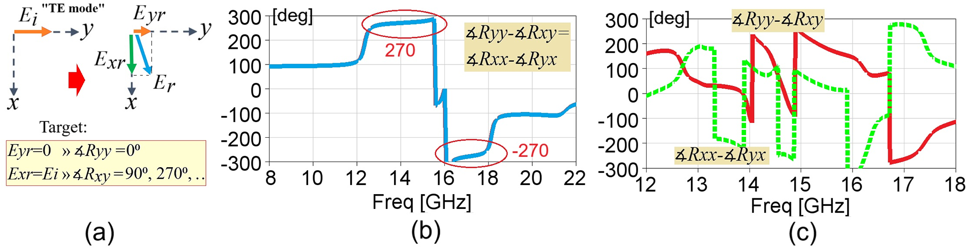
To demonstrate co-to-cross-polarization conversion, the reflection components’ phases are crucial, as simplified in Fig. 6(a). For TM-polarized incident (Ei along y-axis), the reflected field (Er) has both vertical components, Eyr and Exr. Ideal conversion requires a 90° rotation (Exr only) and thus,  ${R_{yy}}\,$should be zero. The phase of
 ${R_{xy}}$should be odd multiples of 90° for rotation, while 0° or 180° implies no rotation. Figures 6(b) and (c) show reflection-coefficients phase differences for [Reference Khanna and Awasthi19] and [Reference Amugothu and Damera20], respectively. Due to symmetry, paper [Reference Khanna and Awasthi19] exhibits ±270° phase differences in 12–18 GHz range, validating conversion from co to cross. Reference [Reference Amugothu and Damera20] shows ±90° around 14 GHz and +90°/+270° around 15.2 GHz, while outside these ranges, phase differences are near 0° or ±180°, indicating no rotation.
(a) Phase target for reflection parameters, (b) the phase difference between corrected reflection parameters for [Reference Khanna and Awasthi19], and (c) the phase difference between corrected reflection parameters for [Reference Amugothu and Damera20].

Conclusion and recommendation for improving [Reference Khanna and Awasthi19] and [Reference Amugothu and Damera20]
(1) Based on PCR and phase graphs, ref. [Reference Khanna and Awasthi19] is an effective co-to-cross converter over a wide band, while ref. [Reference Amugothu and Damera20] is a narrow dual-band converter. Neither design is a perfect absorber.
(2) To enhance ref. [Reference Amugothu and Damera20], given its asymmetry for orthogonal incident angles, a two-layer structure using complementary designs is suggested to improve PCR over a broader band. This will enhance polarization conversion but not absorption, as there are no lossy elements.
(3) For ref. [Reference Khanna and Awasthi19], which already has good polarization conversion and wide bandwidth, a binary-coding optimization algorithm (0 and 1) is recommended. Define the original cell as code 0 and its 90° rotated version as code 1. Design a 2 × 2 array structure combining these codes and adjust cell spacing to optimize the array factor for reflection damping. This approach aims to convert single-resonance absorption into overlapped multi-resonance absorption behavior with very-low-loss elements, thus broadening the absorption bandwidth.
(4) In the simulation section, in addition to the previously mentioned points, efforts should be made to define a more precise meshing on the conductor’s surface. More importantly, the convergence process of the software algorithm must be fully completed. In other words, incomplete or weak convergence will lead to erroneous results.

Reza Zaker Associate Professor at Azarbaijan Shahid Madani University (Electrical Eng Department), Tabriz, Iran. A researcher in new printed antennas and arrays, printed active microwave circuits, Metasurfaces and RIS, Anti radar surfaces.