I. INTRODUCTION
This special focus issue is a testament to the recent interest in nanowires, particularly semiconducting nanowires. In addition to improvements for traditional Si–based integrated circuit technology,Reference Nam, Jiang, Xiong, Ham and Lieber1 these structures have potential applications in a broad range of fields including energy productionReference Bierman and Jin2, Reference Kelzenberg, Boettcher, Petykiewicz, Turner-Evans, Putnam, Warren, Spurgeon, Briggs, Lewis and Atwater3 and storage,Reference Chan, Peng, Liu, McIlwrath, Zhang, Huggins and Cui4 sensing of biological molecules,Reference Cui, Wei, Park and Lieber5–Reference Zheng, Patolsky, Cui, Wang and Lieber7 and even the probing of living cellsReference Kim, Ng, Kunitake, Conklin and Yang8, Reference Tian, Cohen-Karni, Qing, Duan, Xie and Lieber9 among many others.
The morphology of these nanostructures must be controlled in order to produce functional devices. The vapor–liquid–solid (VLS) growth mechanism of nanowires, first described in the case of micrometer diameter Au-catalyzed Si whisker growth by Wagner and Ellis,Reference Wagner and Ellis10 is still one of the most popular nanowire fabrication methods. In this growth technique, a precursor gas decomposes and feeds material to a liquid–alloy droplet. The droplet eventually becomes supersaturated, resulting in the growth of a solid crystal with a diameter that is approximately the same as that of the liquid droplet. Growth proceeds with the liquid droplet riding along the tip of the growing crystal as long as the precursor gas is supplied.
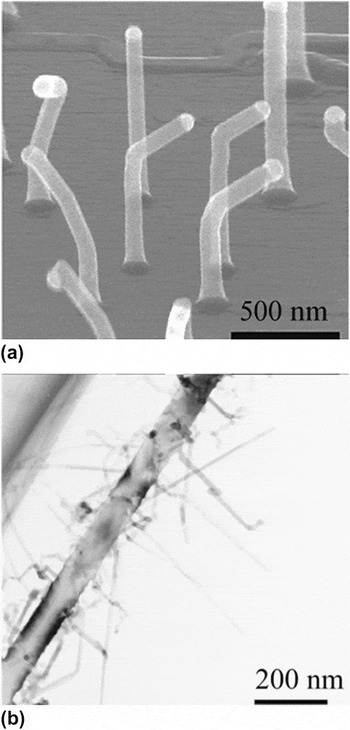
The VLS technique has been popular, in part, because it is capable of producing straight, high aspect ratio, single crystals with few or no defects. However, there are many examples of wires that deviate significantly from this morphology. Reports of complex wire morphology in the Au–Si system date back to some of the earliest studies on their growth more than 40 years ago.Reference Wagner and Doherty11 One common example is “kinking” whereby an otherwise perfectly straight nanowire suddenly changes its growth direction, often from one well-defined crystallographic direction to another as in Fig. 1(a). Another example known as “branching” is a transition from growth along a single direction to simultaneous growth along several directions, which is shown in Fig. 1(b).
(a) Kinked Au catalyzed Si VLS nanowires reported by Madras, Dailey and Drucker. Adapted with permission from Ref. Reference Madras, Dailey and Drucker19, copyright 2009 American Chemical Society. (b) Simultaneous growth of small side branches off of a main Au catalyzed Si nanowire trunk as observed by Kawashima et al. Adapted with permission from Ref. Reference Kawashima, Mizutani, Nakagawa, Torii, Saitoh, Komori and Fujii17, copyright 2008 American Chemical Society.

Kinked or branched nanowires are undesirable for many applications, and thus understanding how and why these structures form is critical to prevent wires with morphological “defects.” There are, however, recent examples where these traditionally unsuitable morphologies lead to performance improvements or even enable completely new device capabilities. A recent review by Bierman and Jin discusses performance improvements in PbS nanowires for solar energy conversion resulting from the use of branched and hyperbranched morphologies as opposed to straight structures.Reference Bierman and Jin2 Side branches enhance light scattering and ultimately result in a higher collection of incident radiation. Tian et al. recently developed nanowire-based sensors capable of probing electrical signals within living cells by employing simultaneous dopant modulation and kink placement.Reference Tian, Cohen-Karni, Qing, Duan, Xie and Lieber9, Reference Tian, Xie, Kempa, Bell and Lieber12 The enhanced spatial resolution of these devices compared to traditional techniques is opening up new windows into inter- and intracellular processes. Clearly, in addition to understanding how and why kinking and branching occur in order to grow straight, high aspect ratio wires, it will be equally important to understand these processes so as to control complex growth morphologies and further enable devices with unique capabilities.
Although kinking and branching have been known about for quite some time, the mechanisms involved are still poorly understood. In the following sections, we describe some of the experimental and theoretical work in the field of Au-catalyzed Si nanowire growth, with emphasis on work involving complex morphologies. In addition, we describe recent phase-field modeling work that we have undertaken to better understand the stability and dynamics of liquid droplets during VLS growth as well as the implications for kinking and branching growth modes.
II. BACKGROUND
A. Experimental
Even by restricting the discussion to the relatively simple case of Au-catalyzed Si wires, there are many experimental variables including precursor gas (e.g., SiCl4, SiH4, Si2H6), total reactor pressure, precursor partial pressure, temperature, other gases in the chamber (e.g., H2, O2, or dopants like PH3 or B2H6), and wire diameter. These quantities can be directly controlled and some can be changed during growth, potentially enabling control over wire morphology. Based on the number of relevant experimental variables, it is no surprise that a wide range of growth behaviors has been reported in the literature.
Wagner and Doherty report extensively on kinking and branching in the early work on the VLS growth of Si wires grown from SiCl4 precursor gas.Reference Wagner and Doherty11 In this work, kinking between 〈111〉 directions as well as between〈111〉 and 〈110〉 type directions was observed. In some cases, they intentionally induced kinking by creating thermal gradients normal to the direction of wire growth. This led to changes in the morphology of the solid–liquid interface and ultimately caused the wire growth direction to change. In addition, rapid temperature changes often triggered kinking or branching, which the authors suggested was due to a change in the volume of the liquid droplet. They argued that the volume increase associated with an increase in growth temperature causes the droplet to spill over onto the side face of the existing wire, thereby initiating a kink. Alternatively, the decrease in volume caused by a temperature reduction leads to an abrupt increase in growth rate that can cause partial droplet breakup and subsequent branching. Bootsma and Gassen also report kinking of Si and Ge wires between 〈111〉 type directions in wires of similar diameter grown with Au catalyst and SiH4 or GeH4 precursors, although no explanation of a mechanism is discussed.Reference Bootsma and Gassen13
The crystals in these early studies are 10s to 100s of micrometers in diameter, several orders of magnitude larger than the wires of interest today. However, similar wire morphologies have recently been observed for wires with diameters of 10s to 100s of nanometers. In addition, a number of experiments have indicated that the pressure of the precursor gas as well as the presence of other gases in the growth chamber are important factors in wire morphology for these smaller wires. It is interesting that both of these variables have been shown to influence the presence and mobility of Au on the sidewalls Si wires.
Fourteen years ago, Westwater et al. reported that growth of Si wires using Au catalysts at high SiH4 pressures and low temperatures resulted in kinked wires.Reference Westwater, Gosain, Tomiya, Usui and Ruda14 Wires 40–100 nm in diameter grew predominantly along the [111] direction at SiH4 partial pressures of 1.3 Pa at 520 °C, whereas at 67 Pa SiH4 and 440 °C they were more likely to spontaneously kink between different 〈111〉 directions. Finally, at 133 Pa and 320 °C, wires grew with almost continuous direction change, although transmission electron microscopy images indicated that they were still crystalline. They noted that the conditions that favored kinking also lead to high growth rates, and they suggested that instability of the liquid–solid interface was an important factor in direction changes.
Although they did not directly report on kinking, Hannon et al. observed that at ultrahigh vacuum conditions (6.7 × 10⁻³ Pa total pressure, 1.3 × 10⁻³ Pa Si2H6, 600 °C), Au can easily diffuse along the sidewalls of growing Si nanowires, ultimately leading to coarsening or Ostwald ripening of liquid Au–Si droplets.Reference Hannon, Kodambaka, Ross and Tromp15 They observed that as Si wires grew in length, larger liquid droplets increased in volume at the expense of smaller neighboring ones, causing significant tapering and ultimately termination of growth for some of the smallest wires. This group also showed that addition of 1.3 × 10⁻⁷ Pa O2 to the chamber dramatically reduced tapering during growth.Reference Kodambaka, Hannon, Tromp and Ross16 Their experiments clearly showed that this was the result of inhibited mobility of Au atoms on the sidewalls of the wires, indicating that even a trace amount of O2 can have a strong effect on the behavior of Au on a Si surface.
Kawashima et al. grew Au-catalyzed Si wires using Si2H6 in H2. They reported that while keeping the partial pressure of Si2H6 constant at 0.27 Pa, growth at 40 Pa total pressure produced straight wires, but at 0.27 Pa total pressure wires were prone to spontaneous kinking.Reference Kawashima, Mizutani, Nakagawa, Torii, Saitoh, Komori and Fujii17 They also did a series of experiments in which the total reactor pressure was constant but the Si2H6 pressure was reduced and found interesting changes in the coverage of Au on wire sidewalls. Specifically, decreasing the Si2H6 partial pressure but keeping the total pressure and temperature constant resulted in significant migration of Au away from the droplet and along the wire surfaces. They further increased the distance that Au migrated away from the droplet after Si2H6 was shut off by decreasing the total reactor pressure to 1.3 × 10⁻⁷ Pa and, conversely, inhibited migration via exposure to air, similar to earlier findings.Reference Hannon, Kodambaka, Ross and Tromp15, Reference Kodambaka, Hannon, Tromp and Ross16 It is interesting that at a pressure of 13 Pa they showed that Au–Si liquid coats the wire sidewalls in the form of small droplets, and they could grow Si nanowires that had many smaller nanowire branches simultaneously growing from the sides. The main backbones were 60–100 nm in diameter and the side branches were 5–25 nm, with the branches highly kinked.
Lugstein et al. grew Si wires with SiH4 in He at 300- and 1500 Pa total pressure with approximately 2% SiH4 at 500 °C at both pressures.Reference Lugstein, Steinmair, Hyun, Hauer, Pongratz and Bertagnolli18 At the lower total pressure (and therefore lower partial pressure) they observed a prevalence of 〈111〉 oriented wires, whereas at the higher pressure the wires grew predominantly along 〈112〉. Furthermore, at higher total pressures the wires were less likely to kink whereas at the lower pressure kinking was more common. It is important that they also showed that they could induce a change in direction from 〈111〉 type to 〈112〉 type by changing the pressure during a growth experiment, indicating that kinks in submicrometer diameter wires can be introduced at a specific point during growth.
Madras, Dailey, and Drucker used undiluted Si2H6 and found that increasing Si wire growth rate by increasing the precursor pressure or decreasing the rate of other activated processes like surface diffusion by decreasing the temperature made spontaneous kinking of Si wires more likely, much like Westwater’s earlier work with SiH4.Reference Madras, Dailey and Drucker19 They also showed that precursor pressure played a critical role in determining toward which direction wires growing along 〈111〉 directions subsequently kinked. Specifically, wires originally growing along the [111] direction kink toward other 〈111〉 directions below a temperature-dependent critical pressure and toward 〈112〉 directions above the critical pressure. Finally, at conditions that favor very high growth rates, the growth direction can change rapidly and nearly continuously in a way that suggests that growth kinetics rather than energetics is dominant, much like the behavior reported by the SiH4 growths performed by Westwater et al.Reference Westwater, Gosain, Tomiya, Usui and Ruda14, Reference Madras, Dailey and Drucker19
Subsequently, this group has shown that the wetting of Au on the sidewalls of wires plays a critical role in the kinking process.Reference Madras, Dailey and Drucker20–Reference Dailey, Madras and Drucker22 Below the temperature-dependent critical pressures that separate the kinking behaviors described above, Au–Si liquid can coat the sidewalls of a 〈111〉 Si wire, reducing the surface energy of the sidewalls and stabilizing the growth direction. At higher pressures, Au–Si liquid dewets from the sidewalls, exposing high energy surfaces, and wires tend to kink away from 〈111〉 directions toward 〈112〉 directions to reduce their energy. They also note that this behavior is the same for both SiH4 and Si2H6 precursor gases, although the Si2H6 pressures for dewetting are 80 times lower than those of SiH4.Reference Madras, Dailey and Drucker20
Although a wide range of experimental conditions has been investigated and different behaviors reported, this body of work as a whole indicates a strong dependence of the kinking and branching behavior on the vapor-phase atmosphere within the growth chamber, in terms of both the precursor pressure as well as other gases. The nature of Au coverage and mobility on the wire sidewalls is also critically important through its effect on the solid–vapor surface energy. The importance of surface energies is a theme that has also been explored using several theoretical and modeling approaches.
B. Modeling and theoretical work
Theoretical approaches have shed light on complex nanowire morphologies. Experimental work has primarily focused on investigating conditions that favor or directly induce kinking, but the theoretical focus has been on analyzing the stability and dynamic transitions of liquid droplets that enable direction changes. For a growth-direction change, there must be a change in the liquid–solid interface morphology, potentially requiring a significant spatial rearrangement of the droplet. The conditions that determine the stability of the liquid droplet at the wire tip therefore constrain kinking, and the dynamics of how the droplet transitions occur can further influence morphological changes.
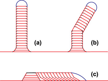
An elegant model that reproduces a wide range of experimentally observed VLS growth behaviors, including kinking, was recently developed by Schwarz and Tersoff.Reference Schwarz and Tersoff23, Reference Schwarz and Tersoff24 In this two-dimensional model, a combination of a mechanical force balance at the VLS contact line and a difference in chemical potential between the liquid and solid phases controls growth of the solid. Furthermore, new facets are introduced at the contact line when energetically favorable. The model predicts that stably growing straight wires [Fig. 2(a)] will kink when the vapor–solid surface energy is briefly perturbed on one side of the wire as in Fig. 2(b), much like Wagner and Doherty’s experimental findings.Reference Wagner and Doherty11 Under other conditions, the model predicts growth-direction changes without applied perturbations before the droplet fully lifts off of the substrate shown in Fig. 2(c). This leads to stably “crawling” wires that grow along the substrate rather than vertically off of it.
Examples of the nanowire morphologies produced by Schwarz and Tersoff’s 2-D model: (a) straight, (b) kinked, and (c) crawling growth modes. Adapted with permission from Ref. Reference Schwarz and Tersoff24, copyright 2011 American Chemical Society.

In all of these results, a morphological transition of the droplet is necessary for a growth-direction change. These transitions require unpinning and subsequent motion of the three-phase contact line from a crystal edge. Although their model does not treat the dynamics of the unpinned contact line, the work highlights the importance of unpinning and contact-line stability on wire morphology. Contact-line motion is certainly rapid on the time scales of techniques typically used to characterize dynamic growth behaviors (e.g., in situ transmission electron microscopy), but the assumption of mechanical equilibrium at all times implies instantaneous relaxation of the contact line. The actual dynamics of contact-line motion could influence the topological pathway that a droplet takes between two energy-minimizing configurations and could ultimately lead to mechanically metastable states not predicted by energy minimization alone.
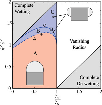
Roper et al. investigated the energies of a number of axisymmetric liquid configurations including the typical droplet on the tip of the wire as well as an annular configuration where the liquid wets only the sides of the wire.Reference Roper, Anderson, Davis and Voorhees25 Using energy arguments, they determined the conditions necessary for steady growth based on the ratios of the solid–vapor and solid–liquid surface energies to that of the liquid–vapor surface energy, which are γsv/γlv and γsl/γlv, respectively. Three important cases are considered in Fig. 3. In regions A and B, steady growth of nanowires from a pinned liquid droplet is possible. However, in region C, the contact line of a liquid droplet on the tip of a wire is unstable with respect to unpinning from the corner of the solid crystal, thus interrupting axial growth. Furthermore, in region B between the solid and dashed curves, while the contact line remains pinned, the droplet configuration actually has a higher total energy than the annular configuration and is thus metastable with respect to the annular arrangement.
Range of surface energy ratios over which stable nanowire growth is possible and schematic energy minimizing liquid configuration adapted from Roper et al.Reference Roper, Anderson, Davis and Voorhees25 In regions A and B, stable nanowire growth is possible, however in region C the contact-line is predicted to unpin from the corner of the solid crystal and instead wet the sidewalls. In region B, stable growth is possible, however the annular configuration has a lower total energy and thus the droplet configuration could be metastable. The open circleReference Schmidt, Senz and Gösele27, squareReference Roper, Davis, Norris, Golovin, Voorhees and Weiss28 and triangleReference Schwarz and Tersoff23 represent approximate values of surface energy of the Au-Si system reported in the literature, and the + is for values reported in Table I.

Although the annular configuration minimizes the total energy in regions B and C, it is quite possible that nonaxisymmetric configurations could further reduce the total energy of the droplet. Application of a planar analysis for a cylindrical fluid in contact with a planar substrate indicates that breakup of the annular liquid along the circumferential direction is likely.Reference McCallum, Voorhees, Miksis, Davis and Wong26
It is interesting that the surface energy values reported for the Au–Si system lie near the transition from stable to unstable droplets, indicating that typical growth configurations might be metastable with respect to changes in droplet morphology.Reference Schwarz and Tersoff23, Reference Roper, Anderson, Davis and Voorhees25, Reference Schmidt, Senz and Gösele27, Reference Roper, Davis, Norris, Golovin, Voorhees and Weiss28 This indicates that slight changes in the surface energies during growth (via changes in the vapor pressure or system temperature, or by the addition of other chemical species among others as indicated by the results in Sec. II. A.) could initiate a transformation in the droplet configuration. The presence of a liquid droplet on the tip of the wire (or lack thereof) is an important factor in the growth of straight wires. Thus, a transition of the droplet from the tip to the side of the growing wire that is due to instability could lead to a growth-direction change or even stop growth altogether.
The analysis underlying Fig. 3 is based on energy minimization and therefore does not include kinetic effects or consider how the transition between two liquid configurations might occur. In order to address these added complexities as well as the time scales over which droplet rearrangement occurs, a fully time-dependent model that accounts for fluid flow is necessary. To that end, we employ a phase-field model that accounts for viscous fluid flow as well as diffusive mass transport and crystal growth in a system with three phases and two alloy components. However, we first consider the dynamics of moving liquid droplets.
C. Droplet dynamics
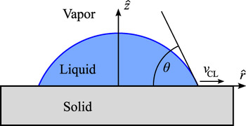
The fluid dynamics of moving contact lines has been extensively studied analytically and experimentally in the context of spreading liquid droplets on planar substrates.29–31 A droplet contacting a substrate with a contact angle θ that is different from its equilibrium contact angle θe will spread or contract because of an imbalance of forces in the plane of the substrate, as depicted in Fig. 4. If θ > θe, the droplet will spread with a contact line speed v CL > 0 conversely, when θ < θe the droplet retracts and v CL < 0. Rosenblat and Davis treat the spreading of a droplet across an inert, planar substrate analytically and investigate a case where v CL is linearly proportional to the deviation of θ from θe,

Schematic of a droplet on a planar substrate. We use a cylindrically symmetric coordinate system with  and
 as unit vectors in the radial and axial directions respectively. The instantaneous contact angle is θ and the contact line velocity is v CL. For a retracting droplet, v CL < 0.

where κ is a constant with units of velocity per radian.Reference Rosenblat, Davis, Davis and Lumley32 This relationship implies that v CL goes to zero when θ = θe. In addition, there are a number of theories regarding the atomic-scale mechanisms that determine κ, as well as other functional forms that relate v CL and θ; however, the details of these are beyond the scope of the present work.Reference de Gennes30, Reference Blake31, Reference Blake and Haynes33–Reference Hoffman36
In analytical solutions for droplet evolution, the behavior of a spreading droplet is characterized by the nondimensional quantityReference Rosenblat, Davis, Davis and Lumley32

where ηl is the dynamic viscosity of the liquid, γlv is the liquid–vapor surface energy, and κ is the constant from Eq. (1) (we use the subscript 1 to differentiate this quantity from the more common capillary number C discussed shortly). For systems where C1 ≪ 1, there is an initial adjustment in the shape of the droplet driven by nonconstant curvature of the liquid–vapor interface while the contact line remains approximately stationary, which is referred to as “capillary push.” This is followed by a longer period where the contact line moves and contact angle slowly relaxes to θe, which is referred to as “contact line pull.” Conversely, when C1 ≪ 1, there is rapid initial relaxation of the liquid–vapor interface in the vicinity of the contact line, followed by a slower spreading with an approximately constant contact angle.
There are several other important nondimensional parameters that characterize the relative importance of different physical phenomena in fluid flow in addition to C1. Of particular importance are the so-called Reynolds, Capillary, Weber, and Ohnesorge numbers that are respectively defined as


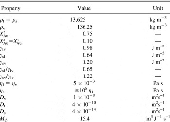
where ρl is the liquid density and R 0 is a characteristic droplet radius. We note that of these quantities, O is the only one that does not depend on v CL, which is not known a priori. With the fluid parameters from Table I and a droplet radius of 25 nm, we find O = 0.27. According to an analysis by Schiaffino and Sonin, a characteristic spreading velocity is thenReference Schiaffino and Sonin37

Physical parameters used in simulations with reported kinetic measurements.

Some simulations are performed with other physical parameters. However, only qualitative results have been reported in those cases. Composition and density values are reported for a system at equilibrium with planar interfaces.
Using this relationship, v CL ≈ 2 m s–1 and we then estimate the remaining nondimensional quantities R = 0.13, C = 0.01, and W = 1.3 × 10⁻³. For W ≪ 1 and O > 0.01, we expect the droplet evolution to be dominated by capillarity driven spreading resisted by viscous forces, with only a minor role played by inertial effects. Thus, we do not expect contact-line oscillations and large variations of the liquid-vapor interface curvature common in the spreading of larger drops with O ≲ 1 × 10⁻³.Reference Wheeler, Warren and Boettinger38
D. Phase-field modeling
The phase-field modeling technique has been successfully employed to investigate a wide range of moving boundary problems relevant to materials science, including solidification of pure materials and alloys, as well as solid-phase transformations such as coarsening and grain growth.Reference Boettinger, Warren, Beckermann and Karma39, Reference Chen40 Phase-field models have also been previously used to study droplet dynamics, although not directly in the context of nanowire growth.Reference Wheeler, Warren and Boettinger38, Reference Seppecher41–Reference Villanueva, Boettinger, Warren and Amberg45 These models can efficiently treat the time evolution of morphologically complex interfaces as well as topological transitions such as contact-line formation.
The phase-field method uses a diffuse-interface approach, which avoids abrupt changes in material properties common to sharp-interface methods by smoothing the property values through the interface region. This makes solving the governing equations much simpler because it eliminates tracking of morphologically complex, moving interfaces. In the limit where the interface thickness is taken to zero, the “sharp-interface” governing equations are recovered.Reference Karma and Rappel46
The phase-field model employed here is based on a model developed by Sekerka and Bi,Reference Sekerka, Bi and McFadden47, Reference Sekerka48 which was recently numerically implemented by Wheeler, Warren, and BoettingerReference Wheeler, Warren and Boettinger38 using FiPy,Reference Guyer, Wheeler and Warren49 a finite volume partial differential equation solver developed at the NIST Center for Theoretical and Computational Materials Science. It incorporates the relevant physical phenomena to simulate nanowire growth and droplet dynamics, namely, viscous fluid flow, phase transformation, diffusive mass transport, and surface energy effects.
Accounting for convective and diffusive mass transport, mass conservation for the alloy component i is expressed

where ρi represents the local mass density of component i,  is the convective velocity vector, and
 is the diffusive mass flux. Finally, Si is a source term that introduces new mass into the system, resulting in growth of the solid phase. In cases with growth, we allow the source terms to be nonzero in a thin region along the top of the computational domain. In addition, we note that the total density ρ is simply the sum of the component densities ρi .
The diffusive mass flux  is proportional to gradients of a nonclassical chemical potential difference

where M ρ is the order-parameter dependent mass mobility that is related to the diffusion coefficient D as discussed in Ref. Reference Wheeler, Warren and Boettinger38. The nonclassical chemical potential  is

where μi is a bulk chemical potential that can be expressed in terms of a molar Helmholtz free energy F m, and ερ is a gradient energy coefficient to be discussed shortly.
In addition to the dependent variables ρi , the model includes an order-parameter field ϕ that takes on the value of 1 in solid regions and 0 in fluid regions (both liquid and vapor). This nonconserved quantity evolves according to an Allen–Cahn equation with the addition of a convective term:

where M ϕ is the mobility of the order-parameter field.
The Navier–Stokes equations ensure a momentum balance as expressed by

where we have neglected body forces and  is the stress tensor,

Here, P is the thermodynamic pressure that can be written in terms of F m,  is the unit tensor, and
 is the deformation rate tensor that has Cartesian components,

Along with initial and boundary conditions and a particular choice of F m (ρ1, ρ2, ϕ), Eqs. (8), (11), and (12) provide a framework for computing the time-dependent densities ρi , velocity  , and order parameter ϕ. The free energy functional F m (details of which appear in Ref. Reference Wheeler, Warren and Boettinger38) supports simultaneous equilibrium between two dense phases, solid and liquid, and a third low-density vapor phase. In addition, the dynamic viscosity η is a function of ϕ:

where ψ = ϕa, and in this work we take a = 1/2. A similar interpolation scheme is used for the mass mobility M ρ.
Finally, we also note that terms in the model proportional to ερ and εϕ give rise to surface energies that ultimately affect the chemical potential through Eq. (10), phase stability through Eq. (11), and state of stress through Eq. (13). These relationships result in realistic interface curvature-dependent shifts in the equilibrium compositions via the Gibbs–Thomson effectReference Adhikari, Marshall, Goldthorpe, Chidsey and McIntyre50–Reference Kim, Tersoff, Wen, Reuter, Stach and Ross52 as well as fluid flow driven by surface tension.
In our simulations we use a cylindrically symmetric coordinate system with radial and axial coordinates  and
 , respectively. This choice allows axisymmetric problems to be described with two spatial coordinates while including nonplanar interface curvature effects. The density fields are subject to no-flux boundary conditions, and the fluid flow obeys a zero shear stress condition on external boundaries. The domain is discretized on a 256 × 256 grid. Further details of the numeric implementation of this model can be found in Ref. Reference Wheeler, Warren and Boettinger38.
E. Physical parameters
The physical parameters used in our simulations are chosen to approximate the Au–Si system and are shown in Table I. The molar mass m is assumed to be the same for both components. The values of m and ρl are chosen using a Vegard’s law approximation for a liquid that is 75% Au, roughly the eutectic composition of the bulk Au–Si phase diagram. The solid phase is assumed to have the same density as the liquid, and the vapor density is chosen to be 100 times less than the solid–liquid density.
In reality there is a large density difference between pure Si and the Au–Si liquid alloy (almost 5×). However, we set these equal because it does not strongly affect the fluid dynamics in the liquid droplet. Setting ρs = ρl eliminates convective currents in the liquid associated with a volume change upon solidification. These convective flows are weak compared to the flows resulting from contact-line driven motion for reasonable solid growth rates. In additon, we note that our choice of ρv = ρl/100 results in a vapor that is significantly more dense than in a typical chemical vapor deposition growth chamber. However, ρv does not strongly affect the liquid flow as long as it is much less than that of the condensed phases, and this particular choice is computationally tractable.
These simulations use a realistic fluid viscosity as listed in Table I, and the solid viscosity is a factor of at least 106 larger. Despite this large change in viscosity across the liquid–solid interface, the solid viscosity is still orders of magnitude lower than an actual solid.Reference Iida and Guthrie53 However, we find that the flow velocity in the solid is still essentially zero, indicating that the factor of 106 increase in viscosity is large enough to capture realistic solid behavior over the time scales of these simulations. Further increasing the solid viscosity beyond 106 ηl does not affect the liquid flow field on the time scales of our simulations.
The physical quantities listed in Table I are for a system at equilibrium with planar interfaces. The values of composition and to a lesser extent density are shifted according to the Gibbs–Thomson effect for simulations with a finite radius of curvature. These changes can affect the values of surface energy, although the shifts are typically within 10% of the values listed in Table I. Finally, we note that in some calculations parameters other than those listed in Table I were employed for numerical efficiency. In these cases, we report qualitative results only.
III. PHASE-FIELD MODELING RESULTS
We investigate a range of dynamic droplet behaviors relevant to VLS nanowire growth using the model outlined in the previous section. We first look at a system with a spherical solid particle on an inert substrate surrounded by a liquid-alloy droplet. We perturb the shape of the droplet and find that the droplet dewets the substrate and ends up sitting on top of the solid, much like the liquid must do as a solid wire begins to grow vertically off of a substrate. We next look at a similar transition that is induced by growth of the solid crystal rather than an applied perturbation. Then we consider the effects of anisotropic growth of the solid phase on the dewetting and show that different droplet topologies are possible when strong anisotropy is present. Finally, we discuss the implications of this work on the stability of droplets during VLS growth and outline a way of testing the theoretical predictions made in Fig. 3.
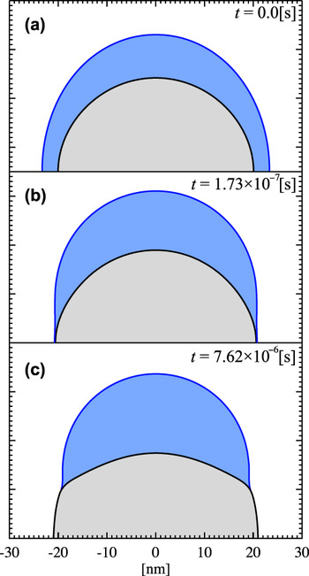
We investigate a simple topological change in a droplet by directly applying a perturbation to an initially spherically symmetric system. We start with an initial hemispherical solid nucleus of radius 20 nm on an inert substrate (the bottom of the simulation domain) and add an ellipsoidal liquid droplet with minor axis 25 nm in the radial direction and major axis 30 nm along the axial direction as shown in Fig. 5(a). This slight initial contraction in the radial direction puts the liquid–vapor and solid–liquid interfaces in a configuration where their diffuse interface profiles slightly overlap, allowing them to interact. This interaction causes a further contraction of the liquid in the radial direction as the simulation begins. We note that this motion is in a direction against the pressure gradient in the liquid caused by the nonconstant curvature of the ellipsoidal liquid–vapor interface. After a short time, the liquid–vapor–substrate contact line intersects the liquid–solid–substrate contact line and a three phase VLS contact line is formed [Fig. 5(b)]. This contact line is not at its equilibrium angle θe, and thus it moves in response to an imbalance of forces. Eventually, the contact line comes to a position where θ ≈ θe and the contact line stops moving [Fig. 5(c)]. This whole process takes place on the order of 1μs in our simulations.
Representative contours which lie within the diffuse interface region of the order parameter (black) and density field (blue) at several times during dewetting. The initial liquid droplet is ellipsoidal with major axis 30 nm in the  direction and minor axis 25 nm in
 The full simulation domain is 64 × 64 nm, and horizontal black lines represents the inert substrate which is also the bottom of the simulation domain.

The rapid contact-line motion is driven by the convective mass flux  . Streamlines of the convective flux in the liquid at the same time as Fig. 5(b) are shown in Fig 6. (Recall that streamlines are instantaneously tangent to the vector field and for unsteady flow they are different from pathlines that trace out the trajectories of individual fluid elements. See e.g., Ref. Reference Malvern54). The flow field in the liquid and vapor phases is much like that described from experimental observation of retracting contact lines as well as sharp-interface analytical results.Reference Dussan V and Davis55 In the liquid, the convective flux carries material away from the contact line and toward the top of the droplet. In the surrounding vapor, mass moves axially away from the top of the upward moving droplet. In addition, vapor flows radially inward toward the retracting contact line as liquid is convected away toward the top of the droplet.
Streamlines of the convective flux field  in the liquid phase at the instant shown in Fig. 5(b). This plot shows 2 contours of the ρ field (blue lines), and the region between them is the diffuse liquid-vapor interface. There is strong flow from the contact line towards the top of the droplet. The flow field is radially symmetric, and for clarity only half of the droplet is shown. The full simulation domain is 64 × 64 nm.

The dynamics of the dewetting process can be established by measuring the contact-line velocity v CL and the instantaneous contact angle θ. However, accurate measurement of contact angles from diffuse interface models is challenging. Here, we employ a simple numerical technique designed to give an estimate of the contact angle. The technique is prone to errors that increase as the radii of curvature of the interfaces decrease with respect to the interface thickness. Furthermore, there is some ambiguity as to the exact location of the contact line with a diffuse interface model that contributes to error in θ measurements. We estimate that this numerical technique is accurate to within approximately 10°. Despite this error, we can still get an order of magnitude approximation of κ in Eq. (1) and ultimately C1 that allows us to compare the behavior of our simulations with predictions from sharp-interface analytical results.Reference Rosenblat, Davis, Davis and Lumley32
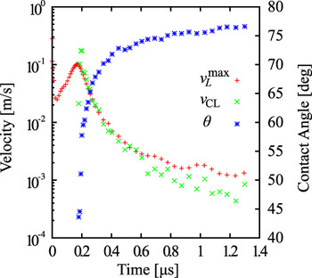
In order to measure v CL and θ, we first estimate the contact-line position by finding a point that has a specific ρ, ϕ, and X combination that is characteristic of an equilibrium contact line. This process is repeated at subsequent time steps and the instantaneous value of v CL is approximated as the change in contact-line position divided by the time elapsed between steps. This technique is inaccurate during contact-line formation, and the contact line must move far enough during a step for the velocity to be measurable. A plot of the magnitude of v CL as well as the maximum fluid flow speed  is provided in Fig. 7.
Maximum liquid flow speed  , contact-line velocity v CL magnitude, and instantaneous contact-angle θ as a function of time during dewetting and droplet formation. While this shows the magnitude of v CL, we note that the contact line is retracting and thus v CL < 0.

At the relatively early times, there is no solid–liquid–vapor contact line, and thus no value of v CL is plotted. After the initial formation of the contact line, v CL tracks the maximum liquid speed quite well, which is consistent with the convective mass flux driving contact-line motion. In addition, the contact-line speed monotonically decays and never changes sign, indicating that there are no oscillations in its position. The peak contact-line and fluid-flow speeds are approximately 0.1 m s−1, which roughly agrees with the prediction in Sec. C. With this value and the appropriate physical values from Table I, the empirically determined values of the nondimensional quantities as described earlier are R = 6.9 × 10⁻³, C = 5.2 × 10⁻⁴, and W = 3.6 × 10⁻⁶ (recall O = 0.27 is independent of v CL). The low value of W and relatively large value of O are consistent with the absence of contact-line oscillations and large changes in liquid–vapor curvature in our simulation, behaviors that are important in spreading of larger droplets.Reference Wheeler, Warren and Boettinger38, Reference Ding and Spelt42
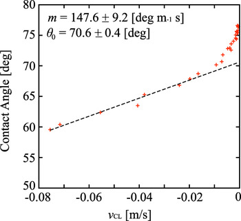
After the contact-line position and velocity are established, the instantaneous contact angle is estimated by placing a circle centered at the contact line and determining the fraction of the area within the circle that has density and order parameters within a range characteristic of the liquid phase. These parameters are calibrated to match both geometric and surface energy based contact-angle measurements to within 10° for static contact lines. We plot θ as a function of v CL in Fig. 8 and use a linear fit to find κ = 0.39 m s−1 rad−1. From this and Eq. (2), we have C1 = 2.0 × 10⁻³, which is consistent with our finding of an initial rapid adjustment in the shape of the droplet due to nonconstant curvature followed by a slower adjustment driven by a nonequilibrium contact angle characteristic of C1 ≪ 1.
Contact-angle θ as a function of contact-line velocity v CL with a fit to κ from Eq. (1). Note that v CL < 0 implies dewetting or contracting rather than spreading of the liquid phase.

The solid phase cannot deform via convective flow because of its high viscosity. The contact line will then move until the contact angle is such that a one-dimensional energy balance is satisfied in a plane tangent to the solid surface:

However, even when Eq. (16) is satisfied, there will still be an imbalance of forces in two dimensions and ultimately a chemical potential imbalance. While convective flow is prohibited, the solid phase can undergo shape changes via phase transformation, an effect that is accounted for in the model. This process is typically slower than convective flow because it involves diffusion, and there will be an initial period where the contact line moves quickly because of the imbalance alone. In the long time limit, however, the shape of the solid changes because of phase transformation and a true two-dimensional force balance and chemical potential balance is approached. The nonconstant curvature in the ϕ contour of Fig. 5(c), particularly near the contact line, is a result of phase change. Past analytical fluid-flow analyses assume an inert and completely rigid substrate. Therefore, we only fit data points in Fig. 8 at times before significant phase transformation occurs (i.e., large v CL). The increase of θ at v CL < 10−2 m s−1 is attributable to phase change and is therefore not included in the fit for κ.
In addition to initiating a dewetting event via an applied perturbation, we also used crystal growth to initiate similar droplet shape changes. The initial conditions are similar to those described for the perturbation initiated dewetting; however, the liquid–vapor interface is spherical instead of ellipsoidal at t = 0. A mass source in the vapor phase, described in Eq. (8), causes convective flux of Si to the liquid. The liquid becomes supersaturated with Si and ultimately the solid crystal grows outward. The liquid volume fraction remains approximately constant during this process; however, the radius of the solid increases and stretches the liquid into a thin concentric film. Eventually, the liquid film breaks at the solid–substrate contact line, forming a solid–liquid–vapor contact line that then dewets as described for the perturbation case. The results are qualitatively and quantitatively similar to the transformations caused by perturbation, the chief difference being that the solid volume fraction increases continuously because of source induced growth.Reference Schwalbach56
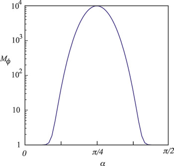
We also find that anisotropic growth can cause droplets to dewet and undergo more extreme topological changes than those described above. Phase-field models can include anisotropy in surface energies as well as in kinetic coefficients,Reference Kobayashi57, Reference Wheeler and McFadden58 both of which are present in real crystals. We introduce anisotropy into our model by making the mobility of the order-parameter field M ϕ dependent on the orientation of the ϕ interface using

where M 1 and M 2 are constants that control the minimum and maximum of M ϕ. The angle α is measured from the  direction to the local solid interface normal and can be computed using the unit normal vector to the ϕ interface:

where  is a unit vector in the axial direction as defined in Fig. 4. Note that α = 0 and α = π/2 correspond to the axial and radial directions, respectively. Because anisotropy is introduced via a kinetic coefficient in this model, the solid phase will exhibit anisotropy only during growth and the equilibrium crystal shape will be unaffected. Finally, in order to emphasize the effects of anisotropic interface shapes on the dewetting process we choose M l = 104 and M 2 = 1, which give M ϕ as shown in Fig. 9. Under these conditions, crystal growth is significantly faster for interfaces with orientations near α = π/4 than in the radial or axial directions.
Anisotropic order parameter mobility defined in Eq. (17) used for the simulation in Fig. 10. α = 0 and α = π/2 correspond to the axial and radial directions respectively. The large change in M ϕ results in significantly faster growth of the solid phase along directions near α = π/4 compared to axial or radial growth.

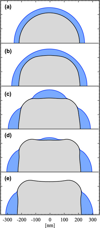
Figure 10 shows a series of cross-sectional snapshots during anisotropic growth. Panel (a) shows the spherically symmetric initial condition, and a short time later panel (b) shows the beginning of anisotropic growth. The crystal has grown more quickly where the interface is oriented with α = π/4, while the liquid–vapor interface remains spherically symmetric. This causes the liquid film to become thinner and eventually leads to pinching of the liquid into two separate liquid volumes visible in panel (c). There is a liquid droplet on top of the crystal as well as an annular liquid volume around the base of the solid. The curvatures of these distinct liquids are different, with the curvature of the droplet being larger than that of the annulus. The droplet then shrinks and the annulus grows via diffusive mass transport, shown in panel (d), and the droplet eventually disappears in panel (e).
Contours of ρ (blue) and ϕ (black) at 5 different times during an anisotropic solid growth. Time increases from (a) to (e) and the solid is shaded gray, liquid blue, and vapor white. The breakup of a liquid droplet into an annulus and droplet due to anisotropic solid growth occurs between (b) and (c). The droplet on top of the solid wire shrinks from (c) to (d) and eventually disappears in (e) due the difference in curvature between the top liquid droplet and annular liquid. The full simulation domain is 600 × 600 nm.

In this particular calculation, solid–vapor and solid–liquid growth kinetics are identical and thus the solid phase continues to grow even after the top droplet disappears. However, in many cases solid–vapor growth is slower than liquid-catalyzed growth by an order of magnitude or more. In such a case, the liquid configuration shown in Fig. 10(e) would not lead to viable nanowire growth. In addition, the present simulation is cylindrically symmetric and thus the liquid state in Fig. 10(e) is stable. However, it is possible that the liquid could undergo a nonaxisymmetric breakup, and a simple extension of a planar calculation indicates that this is likely under the present simulation conditions.Reference McCallum, Voorhees, Miksis, Davis and Wong26 Finally, we point out that Au is known to diffuse quickly on Si under ultrahigh vacuum conditions.Reference Hannon, Kodambaka, Ross and Tromp15 However, it is possible that the Ostwald ripening that occurs between states (c) and (e) could be inhibited if surface diffusion was reduced, such as when O2 is introduced to the growth chamber.Reference Kodambaka, Hannon, Tromp and Ross16
Thus far, our modeling work has allowed us to investigate the dynamics of contact-line motion during droplet configuration changes and substrate dewetting under applied perturbations. We saw good agreement with sharp-interface theoretical predictions as well as qualitative agreement with experimental flow fields. In addition, we demonstrated that solid growth can initiate changes in the droplet configuration and contact-line formation. Finally, anisotropy in the solid–fluid interface can have a dramatic impact on the liquid configurations.
These findings indicate that the phase-field model is a good tool for investigating the stability bounds in Fig. 3 derived by Roper et al.Reference Roper, Anderson, Davis and Voorhees25 By systematically adjusting εϕ and ερ, we found that the relevant range of surface energy ratios can be accessed with our current model,Reference Schwalbach56 whereas these parameters are challenging to control experimentally. Our future work will focus on exploring the stability of droplets and the dynamics of droplet transitions as a function of the relevant surface energy ratios.
IV. CONCLUSION
Experimental studies within the Au–Si system have thus far yielded a wide range of wire morphologies from straight to kinked and even highly branched structures. Althrough there is a broad experimental parameter space to explore, recent work has highlighted the importance of the vapor environment, specifically the precursor and impurity partial pressures, on kinking behavior. These parameters influence the degree to which the Au–Si liquid phase can wet the sidewalls of Si nanowires, affecting the solid–vapor surface energy. This behavior has been carefully studied in the case of Au–Si, but other catalysts or wire materials as well as different dopants or impurities in the vapor phase could all play an important future role.
Theoretical approaches to elucidate the mechanisms behind morphological complexity in nanowires have also recently made great progress. The elegant model of Schwarz and Tersoff qualitatively reproduced experimental results using two-dimensional simulations and emphasized the importance of the addition of new facets to the growth interface as well as unpinning and motion of the contact line.Reference Schwarz and Tersoff24 The work by Roper et al. established bounds on the stability of axisymmetric droplets in the typical growth configuration based on surface energies; they found that typical Au–Si VLS growth conditions could be metastable or even unstable toward a droplet-shape transition.Reference Roper, Anderson, Davis and Voorhees25 Our dynamic simulations of droplets address questions about how liquid droplets retract during the early stages of growth. Furthermore, these calculations indicate that the phase-field model will be a useful tool for investigating behavior in the regime where a liquid droplet is unstable or metastable toward topology changes shown in Fig. 3. In addition, actual nanowires clearly break the cylindrical symmetry employed in our calculation thus far, and this assumption will have to be relaxed to completely understand the contact-line unpinning process involved in VLS kinking, requiring improvements in the underlying numerical techniques.
ACKNOWLEDGMENTS
This research is supported by National Science Foundation Grant CMMI-0507053. E.J.S. acknowledges support from a National Defense Science and Engineering Graduate Fellowship. Computational resources were provided by the Quest cluster at Northwestern University. The authors acknowledge fruitful discussions with A.M. Anderson, S.M. Roper, and J. Tersoff.