I. INTRODUCTION
Recently, switchable (or reconfigurable) bandpass filters, which allow selecting different passbands, are interesting subject in telecommunication [Reference Tu1–Reference Chen, Wu and Lin5]. On the other hand, one of the activities in the field of microwave bandpass filters is to apply composite right/left handed (CRLH) cells, which support right/left-handed waves for the purpose of miniaturization and rejection's improvement [Reference Studniberg and Eleftheriades6–Reference Karimian and Hu9]. Activities on these filters are mainly divided into two groups. In one group, one or more CRLH cells are series and provide the required passband [Reference Studniberg and Eleftheriades6, Reference Lee and Kahng7] and the other group uses CRLH cells to implement bandpass filters in the form of coupled resonator filters [Reference Jang and Kahng8–Reference Ghahremani and Kamyab10]. This paper relies on the second group.
In this paper, we present a coupled resonator bandpass filter by using CRLH cells with reconfiguration capability for providing two operation modes in two different frequency passbands with three PIN diodes. The general structure of this filter has been presented earlier [Reference Jang and Kahng8, Reference Ghahremani and Kamyab10], where the short-circuited shunt resonators are coupled and by using parasitic parameters of distributed elements, a compact bandpass filter with efficient harmonic rejection is achieved. We have added switch ability property; and have studied the structure of the admittance inverters that includes the effects of parasitic elements of this filter. As our studies reveal, there has not been any attention and precise analysis of the structure of the novel admittance inverter is presented in this paper as well as in similar papers [Reference Jang and Kahng8, Reference Ghahremani and Kamyab10].
In Section II equivalent circuits of CRLH cells are presented and a new structure is proposed for admittance inverters. In Section III the reconfigurable filter's structure is explained. Analysis of the proposed admittance inverter is presented in Section IV. And finally, the design procedures and the results of simulation and measurements of this filter are presented in Section V.
II. SYMMETRIC CRLH CELL
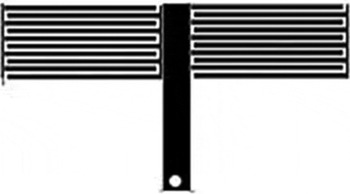
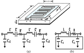
First, we consider a microstrip symmetric CRLH cell (Fig. 1). Equivalent circuit of interdigital capacitor (IDC) is shown in Figs 2(b) and 2(c) [Reference Bahl11].
Symmetric CRLH cell implemented by microstrip.

(a) IDC, (b) high frequency equivalent circuit, (c) and low frequency equivalent circuit [Reference Bahl11].

Here, we use low frequency equivalent circuit (Fig. 2(c)) for simplicity. As you see in the Fig. 2(c), the equivalent circuit consists of series capacitor C, which forms the main element of the IDC circuit; parasitic series inductance, L; parasitic series resistance, R; and parallel parasitic capacitance, C s ; all of them have been explained and formulized in [Reference Bahl11].
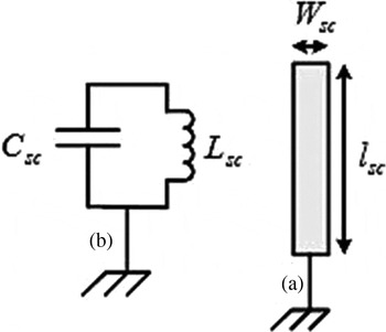
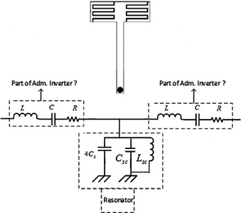
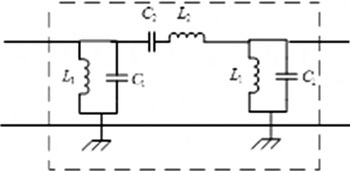
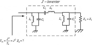
Short-circuited stub is shown in Fig. 3 along with the related equivalent circuit. Some useful equations for calculating C sc and L sc for short-circuited stubs can be found in [Reference Ghahremani and Kamyab10]. So, equivalent circuit of a symmetric CRLH cell would be as in Fig. 4. In that circuit, parallel resonator is realized by the set of parallel capacitance of the short-circuited stub, parallel inductance of the short-circuited stub, and parallel parasitic capacitance of the IDC. On the other hand, the set of the series capacitance of the IDC and parasitic series inductance of the IDC can be introduced as a part of a new admittance inverter (J) and it is named as “Part of Adm. Inverter?” in Fig. 4. So, the circuit of the introduced admittance inverter is shown in Fig. 5 (for lossless case R = 0); the section specified by the name “Part of Adm. Inverter?” in Fig. 4, forms series branch of the admittance inverter in Fig. 5.
Short circuit stub (a), and the related equivalent circuit (b).

Equivalent circuit of a symmetric CRLH cell.

The proposed admittance inverter.

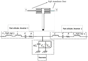
The above admittance inverter must be true in condition of Y in = J 2/Y L , (Y L is the admittance of the load in which circuit of Fig. 5 is ended). According to Figs 4 and 5, the series branch of admittance inverter is formed by a capacitance and an inductance which both are related to the equivalent circuit of the IDC. In other words, IDC enters parasitic inductance and capacitance with specific values into the circuit of Fig. 4; but the values may not be true in the Y in = J 2/Y L ! So, it seems that the high impedance lines between CRLH cells in [Reference Lin, Wang, You and Chang3], provides the required series inductance in the admittance inverter circuit, for satisfying the condition of Y in = J 2/Y L (Fig. 6). Thus, we consider Fig. 6 instead of Fig. 4. The proposed admittance inverter is studied in Section IV in detail.
Equivalent circuit of CRLH and high impedance lines.

III. THE PROPOSED BANDPASS FILTER (TWO-STATES)
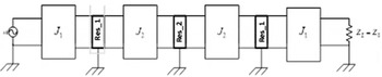
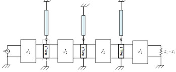
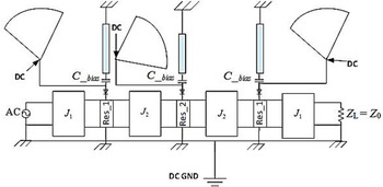
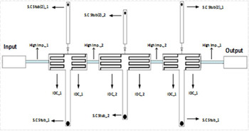
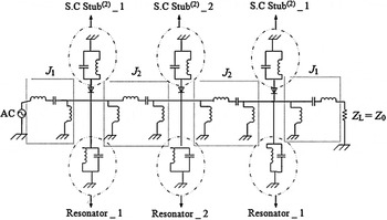
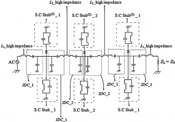
The one-state and the proposed two-states, third-order, bandpass filter have the following diagrams in Figs 7 and 8. The model of the switchable filter with DC bias circuit and the microstrip implementation of the switchable filter without its DC biases is shown in Figs 9 and 10, respectively. This symmetrical filter is a coupled resonator filter composed of shunt LC resonators alternate with admittance inverters (J). The admittance inverter constants are [Reference Pozar12]:
 $${Z_0}{J_1} = \sqrt {\displaystyle{{\pi {\rm \Delta}} \over {2{g_1}}}}, $$
 $${Z_0}{J_2} = \displaystyle{{\pi {\rm \Delta}} \over {2\,\sqrt {{g_1}{g_2}}}}. $$
A coupled resonator, third-order, bandpass filter diagram.

The proposed two-state, third-order bandpass filter diagram.

The proposed two-state, third-order, bandpass filter diagram with bias network.

Filter realization in microstrip technology.

As we know, g 1 and g 2 are the normalized low-pass prototype element values in the filter design by the “insertion loss method” [Reference Pozar12].
Figure 8 is the diagram of our switchable filter; in the ideal case, when all the PIN diodes are off and the extra short-circuited stubs are out of the circuit. So, short-circuited resonators and admittance inverters are designed for the first passband of the filter. When PIN diodes become on, the circuit contains extra short-circuited stubs. These extra stubs should be designed so that the circuit provides the filter function in the second passband.
IV. ANALYSIS OF ADMITTANCE INVERTERS STRUCTURE
The structure of the central admittance inverter in Fig. 8, J 2, is shown in Fig. 11. Indices 1 and 2 for series and parallel components are not related to cells’ number in Figs 7–10; it is just used for simplicity of mathematical equations related to Figs 11 and 12.
Circuit diagram of central admittance inverter, J 2 in Fig. 8.

Circuit diagram of first and last admittance inverters of Fig. 8, J 1.

The central admittance inverter circuit ends in a load impedance of Z L which is, Z L = Z 0, (Y L = 1/Z L ), we want to know the value of the admittance inverter J, for satisfying Y in = J 2/Y L . Input admittance can be achieved through equation (3); where the numerator and denominator are as (4) and (5) respectively:
 $$\eqalign{ {Y_{in}} & = {\left[ {{{\left( {\displaystyle{1 \over {{Z_0}}} + j\omega {C_1} + \displaystyle{1 \over {j\omega {L_1}}}} \right)}^{ - 1}} + j\omega {L_2} + \displaystyle{1 \over {j\omega {C_2}}}} \right]^{ - 1}} \cr & \quad + j\omega \,{C_1} + {1 / {(j\omega {\kern 1pt} {L_1})}} = {{NUM} / {DEN}},} $$
 $$\eqalign{NUM & = {Z_0}[{\omega ^6}\left( {C_1^2 {\kern 1pt} {C_2}{\kern 1pt} L_1^2 {\kern 1pt} {L_2}} \right) \cr & \quad + {\omega ^4}{\kern 1pt} \left( {2{C_1}{\kern 1pt} {C_2}{\kern 1pt} {L_1}{\kern 1pt} {L_2} + C_1^2 {\kern 1pt} L_1^2 + 2{\kern 1pt} {C_1}{\kern 1pt} {C_2}{\kern 1pt} L_1^2} \right) \cr & \quad - {\omega ^2}{\kern 1pt} \left( {2{\kern 1pt} {C_2}{\kern 1pt} {L_1} + 2{\kern 1pt} {C_1}{\kern 1pt} {L_1} + {C_2}{\kern 1pt} {L_2}} \right)\left. { + 1} \right] \cr & \quad + j\omega {\kern 1pt} {L_1}{\kern 1pt} [{\omega ^4}{\kern 1pt} {C_1}{\kern 1pt} {C_2}{\kern 1pt} L{}_1{\kern 1pt} {L_2} \cr & \quad - {\omega ^2}{\kern 1pt} \left( {{C_1}{\kern 1pt} {L_1} + {C_2}{\kern 1pt} {L_1} + {C_2}{\kern 1pt} {L_2}} \right) + 1],} $$
 $$\eqalign{ DEN & = {\omega ^2}{\kern 1pt} L_1^2 {\kern 1pt} \left[ {{\omega ^2}{\kern 1pt} {C_2}{\kern 1pt} {L_2} - 1} \right]{\kern 1pt} \left( {1 + j{\kern 1pt} {Z_0}{\kern 1pt} \omega {\kern 1pt} {C_1}} \right) \cr & \quad + j{\kern 1pt} {Z_0}{\kern 1pt} \omega {\kern 1pt} {L_1}{\kern 1pt} \left[ { - {\omega ^2}{\kern 1pt} {C_2}{\kern 1pt} \left( {{L_1} + {L_2}} \right) + 1} \right].} $$
The circuit in Fig. 11 is considered as an admittance inverter, so the input admittance should be a multiple of Z L , (Z L = Z 0). Thus, according to the numerator of Y in , (equation (4)), the imaginary part of it must be zero, then:
 $${\omega ^4}{C_1}{\kern 1pt} {C_2}{\kern 1pt} L{}_1{\kern 1pt} {L_2} - {\omega ^2}\left( {{C_1}{L_1} + {C_2}{L_1} + {C_2}{L_2}} \right) + 1 = 0.$$
By using equation (6) in equation (5), DEN becomes as below:
 $$DEN = {\omega ^2}{\kern 1pt} L_1^2 {\kern 1pt} \left[ {{\omega ^2}{\kern 1pt} {C_2}{\kern 1pt} {L_2} - 1} \right],$$
and the equation (4) is simplified as:
 $$NUM = {Z_0}\left[ {2{\omega ^6}C_1^2 {C_2}L_1^2 {L_2} + {\omega ^2}{C_2}{L_1}\left. {\left( {{\omega ^2}{C_1}{L_1} - 1} \right)} \right]} \right..$$
If
 $({{1 - {\omega ^2}{\kern 1pt} {C_1}{\kern 1pt} {L_1})} / {{L_1}}}$
in the equation (6) is replaced by an equivalent amount, the value of admittance inverter is:
 $$J{}_{({J_2}\;{\rm in}\;{\rm Fig}{\rm.} \;{\rm 8})} = \sqrt {\displaystyle{{2{\omega ^4}(C_1^2 {C_2}{L_2})} \over {{\omega ^2}{C_2}{L_2} - 1}} + \displaystyle{{{\omega ^2}C_2^2} \over {{{({\omega ^2}{C_2}{L_2} - 1)}^2}}}}. $$
The circuit of the first and last admittance inverters (J 1) of Fig. 8, is shown in Fig. 12. In a similar way, the value of admittance inverter J 1 is achieved as below:
 $$J{}_{({J_1}\;{\rm in}\;{\rm Fig}{\rm.} \;8)} = {{\omega {C_2}} / {\sqrt {{{\left( {{\omega ^2}{C_2}{L_2} - 1} \right)}^2} + {{\left( {{Z_0}\omega {C_2}} \right)}^2}}}}. $$
It can be simply shown that the values of famous purely capacitive or purely inductive admittance inverters could be found via equations (9) and (10); In other words, if we assume that L 2 = 0, L 1 → ∞ and C 2 = −C 1 = C, C > 0 in Fig. 11 (purely capacitive admittance inverter), J (J 2 in Fig. 8) in equation (9) becomes ±ω C. If we assume that C 1 = 0, C 2 → ∞ and L 2 = −L 1 = L, L > 0 in Fig. 11, (purely inductive admittance inverter), J (J 2 in Fig. 8) in equation (9) becomes ± 1/ω L [Reference Pozar12].
Now we have two equations (equation (6) with equation (9) for J
2 in Fig. 8 and equation (6) with equation (10) for J
1 in Fig. 8) and four unknowns (C
1, C
2, L
1, L
2) for each inverter of Figs 11 and 12 (J
1 and J
2 in Fig. 8).Therefore, we consider parallel capacitors of Figs 11 and 12 equal to zero; it means that capacitance branches are open. Moreover, we did not attempt to achieve L
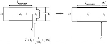
1 in the two figures (Figs 11 and 12); because – as we know from microwave theory – parallel branches of inverters actually do not have any physical appearance in the circuit of the filter. They produce a phase which only affects the phase of resonators. So, if the phase could be achieved, there would be no need to C
1 and L
1 values. We have modeled that phase in Fig. 13, and as a length change in resonator, Δl. The value of Δl is calculated through equating two circuits shown in Fig. 13 [Reference Pozar12]. Also, we replace
 $({{1 - {\omega ^2}{\kern 1pt} {C_1}{\kern 1pt} {L_1})} / {{L_1}}}$
with its equal value from the equation (6):
 $${{\tan \left( {\beta {\kern 1pt} \Delta l} \right)} / {{Z_0}}} = {{\omega \,{C_2}} / {[{\omega ^2}\,{C_2}\,{L_2} - 1}}].$$
Change in resonant stub length caused by shunt components.

Equation (11) reveals that Δl does not depend on parallel elements (C 1, L 1 in Figs 11 and 12). Therefore, C 1 is assumed to be zero and then we apply equation (11) to calculate Δl, and there is no need to know the value of L 1.
V. FILTER DESIGN PROCEDURES
Figures 14 and 15 are equivalent circuits of Figs 8 and 10, respectively.
Equivalent circuits of Fig. 8.

Equivalent circuits of Fig. 10.

As we mentioned before, we assume parallel capacitance of the admittance inverters as zero. Comparison of Figs 14 and 15 helps the design. For the first state of the filter, we must have the values of series admittance inverters’ components; for this purpose, we assume that the coupling is purely capacitive. Then we do the following steps:
-
Step 1: with Δ1 = 0.11 and f 1 = 1.26 GHz and by using equations (1) and (2) we calculate the values of admittance inverters J 1, J 2.
-
Step 2: initial values of C J1 and C J2 are calculated as follows:
(12) $${C_{J1}} = \displaystyle{{{J_1}} \over {{\omega _1}\sqrt {1 - {{({Z_0}{J_1})}^2}}}}, $$
(13)
$${C_{J2}} = \displaystyle{{{J_2}} \over {{\omega _1}}}.$$
-
Step 3: the IDCs (Fig. 14) are obtained as below:
(14)
$$C_1^{IDC} = {C_{J1}},$$
(15)
$$C_2^{IDC} = \displaystyle{{{C_{J1}}{\kern 1pt}. {\kern 1pt} {C_{J2}}} \over {{C_{J1}} - {C_{J2}}}}.$$
-
Step 4: the parameters of IDCs – such as lengths and width of fingers, the number of fingers, parasitic capacitances and inductances – can be calculated [Reference Bahl11].
-
Step 5: the values of series inductance in the branch of each admittance inverter can be obtained by using equations (9) and (10).
-
Step 6: we find the value of Δl, using equation (11). Thus, reduction of the short-circuit stub length is specified [Reference Pozar12].
-
Step 7: the extra stubs are connected to the main stubs with PIN diodes (MA4P274-1141T). The lengths of extra stubs are determined so that they provide filtering in second state (Figs 14 and 15).


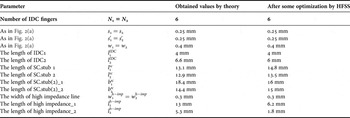
The values of parameters are shown in column (1) of Table 1. Afterwards, we use these values as initial values in a full wave simulator (high frequency structural simulator, HFSS). Then we optimize them to get the proper results (column 2 of Table 1).
The CRLH unit-cells dimensions (on FR-4 substrate with ε r ≈ 4.4, tanδ = 0.02, and 1.6 mm height).

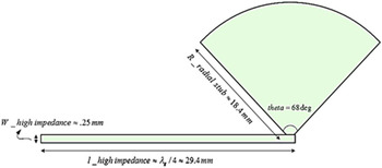
For DC bias network, an inductive quarter wavelength line (λ g /4 high impedance line) followed by a radial stub should be used for each of the extra stubs (Fig. 9). We know that low frequency biasing circuits must be separated from radio frequency (RF) circuit. Hence, it consists of a DC block and an RF choke. DC block is a capacitor and RF choke consists of a high impedance λ g /4 line terminated by an RF bypass capacitor which can be another λ g /4 open circuited line or a radial stub as shown in Fig. 16 [Reference Mongia, Bahl and Bhartia13]. The characteristics of the radial stub could be found via a simple computer simulation (e.g. with Advanced Design System software) by considering that the DC bias circuit must have high input impedance at the second frequency passband.
The DC bias circuit.

Also, we used some capacitors, C_ bias in DC bias network as shown in Fig. 9. These capacitors have large values and they have been used for separating the anodes of diodes from the AC ground of the circuit (ground layer in the bottom of the microstrip substrate) in DC frequency. Their values should be large enough so that in AC frequencies, the capacitors act as small resistors. In simulation, we found that a 5.6 noise figure capacitance as C_ bias is suitable.
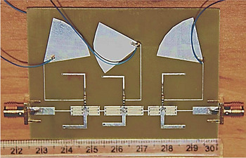
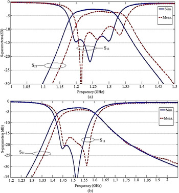
In Fig. 17, the implemented filter has been shown. A FR-4 substrate with ε r ≈ 4.4, tanδ = 0.02, and 1.6 mm height, is used. The dimensions of CRLH unit-cells that are used in fabricated filter are listed in Table 1.The results of simulation and measurements for the first and second state of the proposed switchable filter which are frequency bands of (Δ3dB_1 = 0.11 and f 1 = 1.26 GHz) and (Δ3dB_2 = 0.12 and f 2 = 1.5 GHz), reveal an appropriate accordance, (Fig. 18). If we use a better, low loss substrate, we would have a better transmission loss level in the passbands of the filter.
Implemented filter with FR-4 substrate.

Simulation and measurement results of the first state (a) and second state (b) of the switchable filter.

VI. CONCLUSION
A reconfigurable microstrip coupled-resonator bandpass filter using CRLH cells based on a new kind of admittance inverter was studied. The novel admittance inverter was studied mathematically. The switchable filter was implemented with FR-4 substrate. Results of simulation and measurements had an appropriate accordance with each other.
ACKNOWLEDGEMENT
The authors would like to thank Dr. K. Forooraghi for his measurement setup.
 Samaneh Keshavarzi received her B.Sc. degree in Communication Engineering from the University of Khajenasir Toosi in 2011and M.Sc. degree in Electrical and computer Engineering from the Tarbiat Modares University in 2014, Tehran, Iran. Her main research interests are design and optimization of passive microwave components.
 Zahra Atlasbaf (M'08) received her B.S. degree in Electrical Engineering from the University of Tehran, Iran, and the M.S. and Ph.D. degrees in Electrical Engineering from the University of Tarbiat Modares, Tehran. She is currently an Associate Professor in the faculty of Electrical and Computer Engineering, Tarbiat Modares University. Her research interests include numerical methods in electromagnetics, theory and applications of metamaterials, and microwave and antenna design.