Introduction
Recent advancements in material purification and process optimization using photolithography have led to the rapid growth and application of highly reliable silicon (Si)-based electronic integrated circuits. However, all materials used in such conventional Si-based electronics have focused only on electrical features, but not mechanical features (flexibility and stretchability). These high-purity rigid materials usually exhibit good electronic performance and controllability or stability; however, they exhibit poor mechanical robustness. On the other hand, soft electronic materials show the desired mechanical properties while exhibiting poor electronic properties. Indeed, the maximum conductivity of conducting rubbers comprising carbon particles is 0.1 S/cm, thus making them unsuitable for applications in wiring of integrated circuits.
Recent studies have led to the development of new electronic applications based on the interdisciplinary nature of electronics. This, in turn, has led to the realization of flexible electronics with excellent electronic performance and mechanical stability.Reference Garnier, Hajlaoui, Yassar and Srivastava1–Reference Sekitani, Zaitsu, Noguchi, Ishibe, Takamiya, Sakurai and Someya22 Furthermore, the applications of materials science is not limited to flexible electronics but can be extended to stretchable electronics as well.
The stretchability of electronic circuits can potentially result in the development of a new class of applications, especially in large-area electronics,Reference Garnier, Hajlaoui, Yassar and Srivastava1–Reference Sekitani, Zaitsu, Noguchi, Ishibe, Takamiya, Sakurai and Someya22 because this makes it possible to stretch an electronic circuit over a wide range of curved surfaces and movable parts. In the last decade, thin and lightweight large-area electronic devices have been developed, thereby enabling the placement of solar cellsReference Mitzi, Kosbar, Murray, Copel and Afzali7 and displays on roofs and walls, respectively. Further efforts in enhancing the flexibility of electronic displays are expected to make them bendable and rollable.Reference Cao, Kim, Pimparkar, Kulkarni, Wang, Shim, Roy, Alam and Rogers8–Reference Andersson, Nilsson, Svensson, Chen, Malmström, Remonen, Kugler and Berggren16 Large-area sensors,Reference Someya, Sekitani, Iba, Kato, Kawaguchi and Sakurai17–Reference Someya, Kato, Iba, Noguchi, Sekitani, Kawaguchi and Sakurai19 actuators,Reference Kato, Sekitani, Takamiya, Doi, Asaka, Sakurai and Someya20, Reference Sekitani, Takamiya, Noguchi, Nakano, Kato, Sakurai and Someya21 and memoriesReference Sekitani, Zaitsu, Noguchi, Ishibe, Takamiya, Sakurai and Someya22 are used for embedding intelligence in surfaces. Thus, large-area electronic devices will be further developed to include elasticity; subsequently, it will be possible to place sheet-type devices on curved surfaces.
There are two primary materials challenges in realizing stretchable electronics. One challenge is to ensure the simultaneous achievement of excellent mechanical robustness and electronic performance. To address this issue, various types of highly conductive stretchable materials have been developed, such as three-dimensional (3D) microstructures in poly(dimethylsiloxane) (PDMS), including wavy thin metals,Reference Siegel, Bruzewicz, Weibel and Whitesides23–Reference Brosteaux, Axisa, Gonzalez and Vanfleteren29 metal-coated net films,Reference Someya, Kato, Sekitani, Iba, Noguchi, Murase, Kawaguchi and Sakurai18 graphene films,Reference Kim, Zhao, Jang, Lee, Kim, Kim, Ahn, Kim, Choi and Hong30 and a perforated single-walled carbon nanotube (SWNT)-fluorinated copolymer composite.Reference Sekitani, Noguchi, Hata, Fukushima, Aida and Someya31 These stretchable materials have been used in structures such as waves and nets, owing to their excellent conductivity and mechanical stretchability. Various manufacturing processes have been employed to fabricate the 3D microstructures; these include vacuum evaporation, photolithographic patterning, and mechanical punching and/or cutting.Reference Siegel, Bruzewicz, Weibel and Whitesides23–Reference Sekitani, Noguchi, Hata, Fukushima, Aida and Someya31 The other primary challenge is the integration of electrical and mechanical interconnections between materials whose stiffness values are different by two or three orders of magnitude. In particular, the material interfaces between elastic conducting wiring and electronically active components require high mechanical adhesion as well as good electronic contact.
In this article, we present, as an example, the process of integration of a flexible active matrix comprising organic transistors with elastic conductors for realizing truly rubber-like active matrices for electronic applications.Reference Sekitani, Noguchi, Hata, Fukushima, Aida and Someya31–Reference Sekitani and Someya33 All the materials and manufacturing processes, including elastic conductors as electrical wiring, organic transistors as active components, and the mechanical process described in this review, are applicable to large-area, cost-effective devices.Reference Sekitani, Noguchi, Hata, Fukushima, Aida and Someya31–Reference Sekitani and Someya33 Therefore, our results can significantly expand the scope of flexible electronic applications in daily life. Such applications include electronic artificial skin for future robots; stretchable wires and contacts fabricated from highly elastic conductors and gels in electronic integrated circuits; large-area displays; and the integration of organic circuits with very high-performance silicon-based complementary metal-oxide-semiconductor large-scale integrated circuits.
Perforated active matrix for E-skin
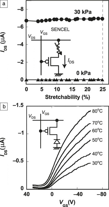
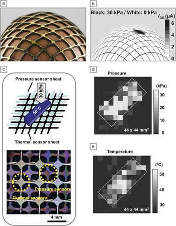
In the future, skin-like sensitivity is expected to be a crucial property for robots to operate in an unstructured environment—the surfaces of the robot are formed by movable and free-formed, curved parts. Flexible, large-area pressure matrices of organic electronic devices have been proposed and developed for use in electronic artificial skin (E-skin) of future-generation robots.Reference Someya, Sekitani, Iba, Kato, Kawaguchi and Sakurai17Figure 1a shows an example of such an application; devices embedded in a plastic film are inherently flexible, and their bendability has been reduced to a radius of 2 mm, which is sufficient for robot fingers. However, human skin is far more complex; in addition to being flexible and pressure sensitive, it performs functions such as thermal sensing with stretchability. Without stretchability, it is not possible to place E-skin on the joints of arms or other curved surfaces of robots. In our study,Reference Someya, Kato, Sekitani, Iba, Noguchi, Murase, Kawaguchi and Sakurai18 we developed stretchable, flexible, large-area E-skin films integrated with organic-semiconductor-based thermal and pressure sensors and a perforated transistor active matrix. A plastic film comprising organic-transistor-based electronic circuits was processed to form a net-like structure; this structure allowed for stretchability of E-skin films by ±25% over the initial length (Figure 1b). The net-like structure was applied to curved surfaces. The electrical performance of the stretchable pressure sensor can be seen in Figure 2. Further, the net-like perforated pressure sensor matrix was stretched over the surface of an egg, which is a good example of a free-form surface, and the corresponding pressure images were obtained (Figure 3).Reference Someya, Kato, Sekitani, Iba, Noguchi, Murase, Kawaguchi and Sakurai18 The spatial distributions of pressure and temperature were obtained using the stretchable active devices.
(a) Image of an electronic artificial skin or E-skin. Organic transistors are employed to realize a flexible active matrix that is used to read out pressure images from the sensors. The device is bendable since all the layers are made of soft materials. (b) Plastic film with organic transistors, pressure sensitive rubber, and thermal sensors is processed mechanically to form unique net-shaped structures. This makes a film device stretchable by ±25%. A magnified view of the stretched net structure is also shown. Organic transistors are positioned at the intersection areas of the net-shaped structure. (c) Circuit diagram of the pressure and thermal sensor matrix. A word line is connected to the gate electrodes, while a bit line is connected to the drain electrodes. The circuit diagram of the thermal sensor matrix can be obtained when the resistances are replaced with diodes. Adapted from References Reference Someya, Sekitani, Iba, Kato, Kawaguchi and Sakurai17 and Reference Someya, Kato, Sekitani, Iba, Noguchi, Murase, Kawaguchi and Sakurai18. ©2004 and 2005, National Academy of Sciences.

(a) Drain current I DS (at drain-source voltage V DS = gate-source voltage V GS = –40 V) with (30 kPa) and without (0 kPa) application of pressure is monitored as a function of stretchability. The dashed line represents the device failure tension. The current (I DS) changes when mechanical pressure is applied to the pressure-sensitive rubber. The inset shows the circuit diagram of one pressure cell (SENCEL) comprising pressure-sensitive rubber and organic transistors. (b) Electrical characteristics of one cell of the thermal sensor network device consisting of diode-based thermal sensors and organic transistors (shown inset) at various temperatures from 30 to 80°C. Adapted from References Reference Someya, Sekitani, Iba, Kato, Kawaguchi and Sakurai17 and Reference Someya, Kato, Sekitani, Iba, Noguchi, Murase, Kawaguchi and Sakurai18. ©2004 and 2005, National Academy of Sciences.

Pressure sensor active matrix stretched over arbitrary curved surfaces. (a) Pressure sensor matrix spread over an egg. (b) Current in each sensor cell (SENCEL) is measured with an applied voltage bias of V DS (drain-source voltage) = –20 V and V GS (gate-source voltage) = –20 V under application of local pressure, and the correct spatial distribution of pressure as current intensity is obtained. (c) Illustration and image of integration of pressure and thermal sensor matrices. (d) and (e) Saturation current, I DS (at V DS = V GS = –40 V) is measured for a SENCEL at various temperatures under application of pressure (30 kPa) and release (0 kPa). A copper block (15 × 37 mm2), whose temperature is maintained at 50°C, is positioned at the center of the array as marked by the dotted line. The sensing area dimensions are 44 × 44 mm2. Adapted from Reference Reference Someya, Kato, Sekitani, Iba, Noguchi, Murase, Kawaguchi and Sakurai18. ©2005, National Academy of Sciences.

Fabrication
An organic transistor active matrix was fabricated on a 75-μm-thick polyimide substrate using vacuum evaporation; subsequently, the matrix was integrated with a sheet of pressure sensitive rubber and a polyethylene naphthalate (PEN) film comprised of a non-patterned Cu electrode.Reference Someya, Kato, Sekitani, Iba, Noguchi, Murase, Kawaguchi and Sakurai18 After the integration (by means of lamination), a section of the sheet device, except the area containing the organic transistors and electrical wiring, was mechanically punched out to form a perforated pressure sensor active matrix.
Stretchability
When the device is stretched, the shape of the net (initially consisting of several small square holes) deforms to diamond-shaped holes, as shown in Figure 1b.Reference Someya, Kato, Sekitani, Iba, Noguchi, Murase, Kawaguchi and Sakurai18 Most of the strain is induced at the base of the current bridges, and its magnitude is small in the transistor regions. Indeed, mechanical and electronic failure always occur around one of the bases of the bridges when tension is applied to the device. One serious concern in the practical application of the stretchable film device may be its mechanical weakness. We tested the mechanical resistance of the device by repeatedly performing strain tests that included a 20% extension of the device and a consequent release of the strain; we found that the device showed no significant electronic degradation even after 1,000 such strain cycles. Therefore, the mechanical resistance of the device is sufficient for many applications requiring a single expansion (e.g., for permanent application on a curved surface). A higher level of mechanical resistance might be required for applications over surfaces such as the joints of arms. This could be obtained if the strain near the bases of the bridges can be suppressed by optimizing structural parameters such as the thickness of the base films and the width of the bridges.
Pressure and temperature sensing
As shown in Figure 3c, the perforated pressure sensors and thermal sensors are positioned alternately at each hole, and each sensor is laminated. This staggered configuration enables the sheets to simultaneously detect pressure and temperature. We applied a mechanical pressure of approximately 30 kPa using a rectangular metal bar at 50°C to the laminated sensors, and we were able to successfully obtain the simultaneous spatial distributions of pressure and temperature. Figure 3d–e shows the electrical performances of the pressure and thermal sensors comprising organic transistors. This indicates the excellent feasibility of using a perforated organic transistor active matrix for displaying sensor readout information.
Rubber-like stretchable organic transistor active matrix using elastic conductors
Although we were able to demonstrate the feasibility of the stretchable organic transistor active matrix as a net-shaped structure (Figures 1–3), several issues regarding the perforated configurations still need to be addressed. For example, the device cannot be stretched biaxially along any axial direction, and its stretchability is limited to 25%–30%. In contrast, a stretchability of 70% is required to simulate the stretching of skin over the curved surfaces of the human body. The limitation of the device’s stretchability to 30% is because the wiring materials (metal-coated plastic film) used thus far is not inherently stretchable.
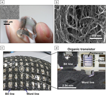
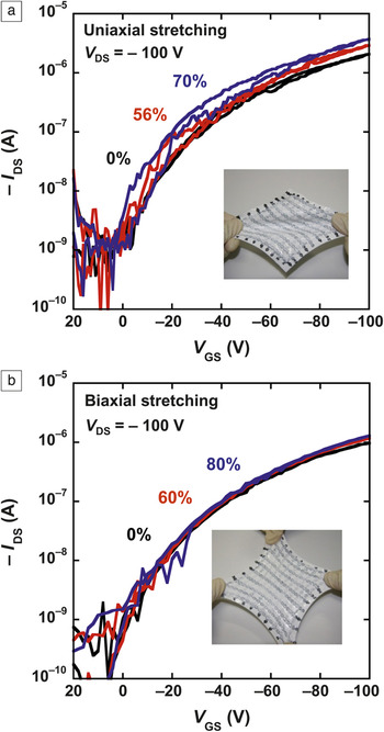
In this section, we describe the fabrication of truly rubber-like integrated circuits by integrating a variety of materials ranging from rigid and semi-rigid elastomers to gelsReference Sekitani, Noguchi, Hata, Fukushima, Aida and Someya31–Reference Sekitani and Someya33 with electrical and electronic circuits. In particular, we fabricated a highly elastic conductor and gel that can be used as stretchable wires and contacts in elastic integrated circuits. We used a novel process that can uniformly disperse finer bundles of SWNTsReference Iijima and Ichihashi34, Reference Hata, Futaba, Mizuno, Namai, Yumura and Iijima35 in a rubber matrix without reducing the length of the nanotubes. In the process, the viscosity of the SWNT-rubber composite gel increased; this material was used to create finely patterned elastic conductors by using direct printing technologies (Figure 4). The elastic conductors were able to stretch by 118%, and they had an extraordinarily high conductivity of 102 S/cm. The dopant concentration of SWNTs could be increased to 20 wt% without compromising the mechanical flexibility or softness of the copolymer. The elastic conductor was chemically stable, and it adhered well to the base plastic films. The elastic conductors were integrated with printed organic transistors,Reference Sekitani, Zaitsu, Noguchi, Ishibe, Takamiya, Sakurai and Someya22, Reference Noguchi, Sekitani and Someya36, Reference Noguchi, Sekitani and Someya37 and a truly rubber-like active matrix was fabricated. The matrix could be stretched by up to 70% without mechanical or electrical damage (Figure 3). Furthermore, we integrated the printed elastic conductors with organic transistors and organic light-emitting diodes (LEDs) to realize a truly rubber-like active matrix organic LED display (Figures 5–7). A 16 × 16 grid of transistors was used to drive the display, and the effective size of the active matrix was 10 × 10 cm2. The display could be stretched by 30%–50%, and it could be spread over a hemisphere without any mechanical or electrical damage. Furthermore, it remained functional even when it was folded in two or crumpled up, thereby indicating excellent durability. The technical details regarding these stretchable displays are described later in this article. The elastic conductor developed in our study allows for the construction of electronic integrated circuits that can be mounted over curved surfaces and movable parts, such as the joint of a robot’s arm.Reference Sekitani, Noguchi, Hata, Fukushima, Aida and Someya31–Reference Sekitani and Someya33
(a) Image of printed elastic conductors on a poly(dimethylsiloxane) (PDMS) sheet. Printed elastic conductors patterned by screen printing can be stretched by 100% without electrical or mechanical damage. The inset shows a scanning electron microscope (SEM) image of the surface of the printed elastic conductors. The image was obtained when the sheet was not stretched. (b) Magnified SEM image of the elastic conductor. Finer or exfoliated bundles of single-walled carbon nanotubes (SWNTs) were uniformly dispersed in the rubber, and they formed well-developed conducting networks. (c) Images of a large-area stretchable active matrix comprising 19 × 37 printed organic transistors and wiring using SWNT elastic conductors. The printed organic transistors function as active components, while the SWNT elastic conductors function as word lines and bit lines for interconnection among the transistors. The image of the matrix was obtained when stretched over a curved surface. (d) Magnified image of one cell. A net-shaped structure comprising SWNT elastic conductors is formed using a mechanical punching system, and it is coated with PDMS. Adapted from Reference Reference Sekitani, Noguchi, Hata, Fukushima, Aida and Someya31. ©2008, American Association for the Advancement of Science.

Transistor characteristics measured under (a) uniaxial stretching values of 0% (black), 56% (red), and 70% (blue) and (b) biaxial stretching values of 0% (black), 60% (red), and 80% (blue). Insets represent images of the stretched active matrix. Adapted from Reference Reference Sekitani, Noguchi, Hata, Fukushima, Aida and Someya31. ©2008, American Association for the Advancement of Science. Note: I DS, drain current; V DS, drain-source voltage; and V GS, gate-source voltage.

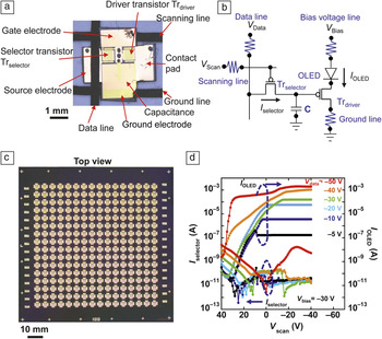
(a) Image of one organic driving cell comprising two organic transistors (2T) and one capacitor (1C). Data, ground, and scanning lines are formed using elastic conductors. The contact pad is connected to the organic light-emitting diode (LED). (b) A circuit diagram of one display cell comprising a 2T1C driving cell and an organic LED. (c) Top view image of the organic transistor array comprising 16 × 16 (512) driving cells. (d) Electrical characteristics of a 2T1C organic driving cell. Currents through selector transistors (I selector) and currents through organic LEDs (I OLED) are shown as a function of voltages applied to scan lines (V scan) when voltages applied to bias lines (V bias) are constant at –30 V and voltages applied to data lines (V data) are varied from –5 V to –50 V. Adapted from Reference Reference Sekitani, Nakajima, Maeda, Fukushima, Aida, Hata and Someya32. ©2009, Nature Publishing Group.

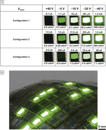
(a) Luminance of a display cell as a function of V scan. Luminance was investigated for three configurations of display cells. Configuration 1: An organic light-emitting diode (LED) integrated with a 2T1C driving cell and electrical wiring composed of 1-μm-thick Cu. Configuration 2: An organic LED integrated with a 2T1C driving cell and electrical wiring composed of printed elastic conductors (conductivity = 50 S/cm). Configuration 3: An organic LED integrated with a 2T1C driving cell and electrical wiring composed of conventional conducting rubber (conductivity = 0.1 S/cm). V bias and V data were maintained at –30 V and –40 V, respectively. I OLED and luminance are also shown for each value of V scan. The effective size of the light-emitting area was 3 × 4 mm2. (b) A stretchable display that can be spread over arbitrary curved surfaces and is functional even when folded in two or crumpled, thereby indicating excellent durability. Adapted from Reference Reference Sekitani, Nakajima, Maeda, Fukushima, Aida, Hata and Someya32. ©2009, Nature Publishing Group.

Matrix fabrication
Figure 4 shows a 19 × 37 organic transistor-based stretchable active matrix fabricated on plastic substrates using printing, vacuum evaporation, and mechanical processes. The fabrication processes and technical details of the printed organic transistor have been reported.Reference Sekitani, Zaitsu, Noguchi, Ishibe, Takamiya, Sakurai and Someya22, Reference Noguchi, Sekitani and Someya36, Reference Noguchi, Sekitani and Someya37 The printed organic transistors exhibited a mobility greater than 0.3 cm2/Vs, and their on/off ratio exceeded 105, thereby indicating good electronic performance. We fabricated an array of organic transistors on a flexible, but non-stretchable substrate. Subsequently, the organic transistors were periodically distributed over a 0.5-mm-thick PDMS rubber substrate using a previously reported mechanical process.Reference Sekitani, Noguchi, Hata, Fukushima, Aida and Someya31 Finally, they were interconnected by means of elastic conductors (bit lines for source electrodes and word lines for gate electrodes). The transistor characteristics did not change after their interconnections via the fabricated elastic conductors.Reference Sekitani, Noguchi, Hata, Fukushima, Aida and Someya31–Reference Sekitani and Someya33 The SWNT elastic conductors were connected to the contact pads for gate, source, and drain electrodes using highly adhesive and conductive SWNT paste comprising SWNTs, rubber matrix, and cross-linkers.
Stretchability of active matrix
The sheet of the active matrix was stretched by increasing the tensile strain, and the transistor characteristics on the stretched sheet were examined (Figure 5).Reference Sekitani, Noguchi, Hata, Fukushima, Aida and Someya31–Reference Sekitani and Someya33 In order to ensure accurate application of uniform strain to the transistor active matrix, we used a small active matrix comprising 10 × 10 cells. Furthermore, we measured the characteristics of the transistor positioned at the center of the matrix, because this transistor was stretched to a greater extent than those at the corners. When the sheet was stretched by up to 70% or less, the change in the transistor characteristics was negligibly small. Subsequently, the strain causing the extension and distortion was removed, and recovery tests for the measurement of the transistor characteristics after relaxation were performed. After the matrix was stretched by up to 70% or less, the transistor characteristics after relaxation did not change when compared to those measured before the stretching tests. Furthermore, no changes were observed in either the electrical characteristics or the mechanical properties of the matrix after 30 stretching cycles at 70% stretching, thereby indicating the excellent electrical functionality and stability of the active matrix under stretching. However, device stretching beyond 70–80% resulted in irreversible degradation. This is mainly due to the exfoliation of the printed Ag electrodes from the plastic substrate. The disconnection of the organic transistors from the SWNT elastic conductor is rare because of the good adhesion provided by the SWNT paste.
Stretchable organic LED display
The benefits provided by stretchable electronics are not limited to sensor applications. Stretchable electronic devices can be used for large-area displays (>10 cm), as mentioned earlier in the article. In the study, we manufactured a rubber-like stretchable active matrix organic LED display comprising 16 × 16 driving cells with two organic transistors and one capacitor (2T1C), organic LEDs, elastic conductors, and paste (Figure 6).Reference Sekitani, Nakajima, Maeda, Fukushima, Aida, Hata and Someya32, Reference Sekitani and Someya33Figure 6 shows images of the sheet comprising 2T1C organic transistor driving cells and the magnified image of one cell. The circuit diagram of one display cell with a 2T1C driving cell and an organic LED is also shown. Each driving cell comprises a selector transistor (Trselector), a driver transistor (Trdriver), a capacitor (C), and printed elastic conductors. The selector transistors allow the addressing of each organic LED for light emission, and the driver transistors control the luminance. The capacitors are required for stabilizing light emission under high-frequency operation. After fabricating the organic LEDs and organic driving cells independently on separate PDMS sheets, the two sheets were laminated to construct a rubber-like stretchable display.
We investigated the electrical characteristics of a 2T1C driving cell with printed elastic conductors. Figure 6d shows the plots of the currents through a selector transistor (I selector) and a driver transistor and organic LEDs (I OLED) as functions of the voltage from the scanning lines (V scan) when the voltages of the data lines (V data) were gradually changed from –5 V to –50 V; the bias voltage of the organic LEDs (V bias) was maintained constant at –30 V. I selector was very small because the selector transistors were not grounded during the application of the voltage V data to the gate electrodes of the driver transistors. Therefore, when one selector transistor is addressed, the connected driver transistor is activated. In fact, I OLED increased from several picoamperes or nanoamperes to several milliamperes with increasing V scan and V data. The on/off ratio of I OLED was found to be 106 when controlling V scan. This result clearly indicates that the driving cells with the 2T1C structure can be used to operate organic LEDs, even large-area organic LEDs that require large currents on the order of several hundreds of microamperes to several milliamperes for light emission.
We next manufactured a 16 × 16-pixel stretchable active matrix organic LED display by integrating a driving cell active matrix and organic LEDs using printed elastic conductors. Figure 7 demonstrates the functioning of the display. This display can be spread over an arbitrary curved surface. Bending or crumpling caused no mechanical or electrical damage because of the excellent conductivity and mechanical durability of the printed elastic conductors, organic transistors, and organic LEDs that were fabricated on PDMS rubber.
Integration of stretchable, large-area, high-performance circuits with Si-LSIs and organic ICs
The integration of organic circuits with very high-performance silicon-based complementary metal-oxide-semiconductor large-scale integrated circuits (Si-CMOS LSIs) can considerably increase the scope of applications utilizing large-area electronics. This is because the operation speed (frequency response) of organic transistors is not very high (as high as MHz range at best) due to the low charge mobility of organic semiconductors (approximately 20 cm2/Vs at best).Reference Fukuda, Sekitani, Yokota, Kuribara, Huang, Sakurai, Zschieschang, Klauk, Ikeda, Kuwabara, Yamamoto, Takimiya, Cheng and Someya38, Reference Minemawari, Yamada, Matsui, Tsutsumi, Haas, Chiba, Kumai and Hasegawa39 In order to demonstrate the feasibility of the direct integration of Si-CMOS LSIs with organic ICs and to utilize the advantages of large-area, stretchable circuits with GHz frequency response, we developed an electromagnetic interference (EMI) measurement sheet integrating organic circuits with excellent mechanical flexibility and silicon (Si) circuits with excellent high-frequency performance (Figures 8–9).Reference Ishida, Masunaga, Zhou, Yasufuku, Sekitani, Zschieschang, Klauk, Takamiya, Someya and Sakurai40, Reference Ishida, Masunaga, Zhou, Yasufuku, Sekitani, Zschieschang, Klauk, Takamiya, Someya and Sakurai41 The stretchable EMI measurement sheet enables the measurement of the EMI distribution on the surface of electronic devices by wrapping the devices with the sheet. The EMI sheet comprises organic transistor-based row decoders, column selectors, Si transistor-based very-large-scale integrated circuits (VLSI), antenna coils, and SWNT-based elastic conductors. The organic-based decoders and selectors work as address and data acquisition circuits, while the Si-based LSIs are required to deal with EMI noise in the frequency range of several hundred MHz or GHz. We first discuss the impetus for this research, then describe the device configuration, and finally summarize the results.
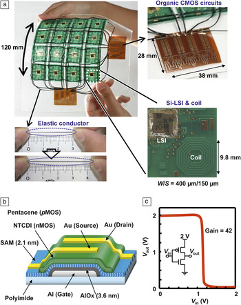
(a) Photograph of a stretchable electromagnetic interference sheet. The top inset shows a magnified picture of an organic complementary metal oxide semiconductor (CMOS) decoder on a polyimide substrate. The bottom inset shows four antenna coils and a silicon-based CMOS large-scale integrated circuit (Si-CMOS LSI) on a printed circuit board (PCB). The diameter of the coil on the PCB is 9.8 mm. (b) Cross-section of organic transistors on a self-assembled monolayer gate dielectric layer. (c) Electrical characteristics of the organic CMOS inverter. Adapted from References Reference Ishida, Masunaga, Zhou, Yasufuku, Sekitani, Zschieschang, Klauk, Takamiya, Someya and Sakurai40 and Reference Ishida, Masunaga, Zhou, Yasufuku, Sekitani, Zschieschang, Klauk, Takamiya, Someya and Sakurai41. ©2009 and 2010, IEEE. Note: NTCDI, naphthalene-1,4,5,8-tetracarboxylic diimide; SAM, self-assembled monolayer; W, line width of antenna coil; S, spacing of lines; V in, input voltage; V out, output voltage.

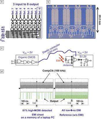
(a) Circuit diagram and (b) image of an organic complementary metal oxide semiconductor (CMOS) 3-to-8 decoder comprising 128 organic CMOS inverters. (c) Schematic illustration of the stretchable electromagnetic interference (EMI) sheet comprising an organic CMOS IC (integrated circuit) as a power supply, an elastic conductor as electrical wiring, and a silicon-based CMOS large-scale integrated circuit (Si-CMOS LSI) as a processor for detecting EMI noise. (d) EMI detection using the proposed scheme. This stretchable system successfully obtained the high-frequency EMI noise. Adapted from References Reference Ishida, Masunaga, Zhou, Yasufuku, Sekitani, Zschieschang, Klauk, Takamiya, Someya and Sakurai40 and Reference Ishida, Masunaga, Zhou, Yasufuku, Sekitani, Zschieschang, Klauk, Takamiya, Someya and Sakurai41. ©2009 and 2010, IEEE. Note: CompClk, comparator’s clock pulse; A0, A2, 2-bit input signal; CSEL, selector signal; Sel 0 to 7, number of output for selectors; V DD, power source voltage.

EMI noise in electronic devices
EMI noise in electronic devices has become a serious problem because of the following three technology trends: (1) use of the same frequency range for radio frequency (rf) signals and clock frequency of digital ICs owing to the increase in the speed of digital circuits, (2) increase in the emitted energy of EMI because of the increased power of LSIs, and (3) increase in the density of LSI packaging. These trends complicate EMI problems and lead to difficulties in the analysis of the root cause of EMI. For example, it is difficult to locate the EMI generation points in electronic devices such as cell phones and PDAs because these devices possess complicated 3D structures. In this study, we examined the feasibility and performance of a stretchable EMI sheet in measuring EMI noise from 3D-structured devices.
Device configuration
Figure 8 shows a photograph of the EMI measurement sheet. The 120 mm × 120 mm sheet has a 4 × 4 printed circuit board (PCB) array and two organic circuits (decoder and selector, referred to as organic ICs in this section). The PCBs and the organic ICs are connected by elastic conductorsReference Sekitani, Noguchi, Hata, Fukushima, Aida and Someya31–Reference Sekitani and Someya33 comprising SWNTs. The whole system is covered with a rubber sheet; this enables the system to be stretched. Each PCB has a 2 × 2 coil array to pick up EMI noise, an LSI, and six stretchable interconnects composed of elastic conductors. The four coils share the LSI to measure EMI. The coils are fabricated on a rigid PCB, because coils on a flexible film provide unstable antenna characteristics due to mechanical bending. Figures 8a and 9a–b show the images of an organic complementary (CMOS) inverter-based 3-to-8 decoder on a polyimide film.
2 V operation of organic transistors and large-area decoders and selectors
Figure 8b shows the cross-section of the organic transistor. The p-type pentacene and n-type naphthalene-1,4,5,8-tetracarboxylic diimide (NTCDI) transistors employed vacuum evaporated aluminum gate electrodes patterned by shadow masking and a gate dielectric based on a combination of a thin layer of aluminum oxide (3.6 nm thick) and a molecular SAM of n-octadecylphosphonic acid (thickness of 2.1 nm).Reference Klauk, Zschieschang, Pflaum and Halik42 The aluminum oxide film was obtained using a brief oxygen plasma treatment that was required to create a sufficient density of hydroxyl groups for molecular adsorption, and the SAM was prepared from a two propanol solution at room temperature. The gate dielectric capacitance was 0.7 μF/cm2; therefore, the thin-film transistors (TFTs) operated at voltages between 2 and 3 V. Pentacene and NTCDI films of 30-nm thickness were deposited in vacuum and patterned by shadow masking to provide the semiconductor films for the p-channel and n-channel transistors, respectively.
P-channel pentacene and n-channel NTCDI transistors with a channel length of 20 μm and a channel width of 50 μm were fabricated on a plastic substrate. Owing to the large capacitance of the thin gate dielectric (0.7 μF/cm2), the pentacene TFTs showed excellent linear and saturation characteristics for gate source and drain source voltages of –2 V. Despite the reduced thickness of the gate dielectric at room temperature, the off state current at gate voltage V GS = 0 V was less than 10 pA, and the on/off current ratio was more than 105. The field-effect mobility of pentacene transistors was more than 0.3 cm2/Vs. The NTCDI transistor had a mobility of 0.02 cm2/Vs and an on/off current ratio greater than 104.
Using p-channel pentacene transistors and n-channel NTCDI transistors with patterned Al gates and a SAM-based gate dielectric on a plastic substrate, we prepared organic CMOS inverters. The circuit diagram and the electrical transfer characteristics of the inverter are shown in Figure 8c. The inverter operates with supply voltages between 1.5 and 2 V and with a small signal gain greater than 42. From a circuit design perspective, complementary circuits have several advantages over circuits based on a single carrier type; these include greater noise margin, lower power consumption, and faster switching speed.
The low-power operating organic CMOS ICs can transmit signals directly to the Si-CMOS LSIs because the operating voltage of organic ICs is the same as that of Si-CMOS LSIs. Almost all organic transistors and circuits require operation voltages more than –40 V, which is too high to integrate with the Si-CMOS LSI, whose operation voltages are less than –3 V. However, these organic transistors can operate within –3 V, due to the use of very thin gate dielectric layers. Figure 9 shows the circuit of the 3-to-8 organic CMOS decoder that comprises 128 organic CMOSs on a flexible plastic substrate.
Si-CMOS LSIs for detection of high-frequency EMI noise
The power supply voltage for both the organic CMOS ICs (row decoders and column selectors) and the Si-CMOS LSI was 2.0 V. The organic circuits and the LSI were connected by 12-cm-stretchable interconnects (elastic conductors) with a width of 1 mm, thickness of 500 μm, resistance of 48 Ω, and resistivity of 0.02 Ωcm. The organic CMOS decoder could successfully drive the LSI. Both the rise time and fall time of the output of the organic decoder were 0.5 s; despite this rise and fall time being considered as slow, it was acceptable for this application.
The typical frequency range for EMI is 30 MHz to 1 GHz, as specified by the International Special Committee on Radio Interference (CISPR). Although the EMI noise power is specified by electric field strength in general, a magnetic field probe with X-Y scanning equipment and a spectrum analyzer are used as an easy EMI measurement method. However, this conventional method is not applicable to 3D-structure devices, since the scanning equipment can only move in a flat plane. Our proposed system was a 3D version of the conventional magnetic field probe system using the coil array. The target noise power was –70 dBm, which is the detectable level of a magnetic field probe.
The Si-CMOS LSI for processing EMI noise comprised four-stage amplifiers, a 0.18-μm Si transistor rectifier, sample and hold circuits, and a comparator. The EMI noise power was rectified by a Si transistor and down-converted into dc voltage and charged in the sample and hold. Therefore, when the antenna coils detected EMI noise, the Si-CMOS LSI output was 2 V dc. Further technical details and the circuit diagram of the Si-CMOS LSI can be obtained from previous reports.Reference Ishida, Masunaga, Zhou, Yasufuku, Sekitani, Zschieschang, Klauk, Takamiya, Someya and Sakurai40, Reference Ishida, Masunaga, Zhou, Yasufuku, Sekitani, Zschieschang, Klauk, Takamiya, Someya and Sakurai41
Demonstration of EMI noise detection
Figure 9c–d demonstrates the EMI measurements obtained from our proposed EMI sheet. We measured the EMI noise around a memory module in a notebook PC. The output spectrum obtained using the magnetic field probe included peak noise power of –50 dBm at 267 MHz. The output obtained from the EMI measurement system showed a high pulse density of 81% at the same place. Without any EMI noise, the output bit stream showed no high pulse; this is shown in Figure 9d. Thus, the proposed stretchable system was successfully able to detect the actual noise emitted by an electronic device.
Our study is the first to demonstrate direct integration between silicon CMOS technology and 2 V organic CMOS technology.Reference Ishida, Masunaga, Zhou, Yasufuku, Sekitani, Zschieschang, Klauk, Takamiya, Someya and Sakurai40,Reference Ishida, Masunaga, Zhou, Yasufuku, Sekitani, Zschieschang, Klauk, Takamiya, Someya and Sakurai41 This integration was possible because we were able to reduce the operation voltage of organic CMOS circuits to 2 V by employing a very thin SAM gate dielectric layer. Furthermore, the stretchable interconnect comprising CNTs allowed the fabrication of a stretchable EMI measurement sheet; subsequently, the stretchable large-area LSI was able to detect EMI noise up to 1 GHz. Because the frequency response of organic circuits is approximately 1 MHz at best, they can detect EMI noise of approximately 1 MHz. However, with the combination of Si-LSI and organic ICs, EMI noise of up to 1 GHz was detected.
Summary
We have outlined the development of a stretchable organic transistor active matrix and how it could be used for large-area electronic applications. Perforated organic transistor active matrices have been realized by employing mechanical processes. A net-shaped pressure sensor matrix was spread over curved surfaces, and the spatial distributions of the mechanical pressure and temperature were clearly obtained simultaneously. We also described the manufacturing of printable elastic conductors comprising single-walled carbon nanotubes uniformly dispersed in a fluorinated rubber. A conductivity of more than 100 S/cm and a stretchability of more than 100% were obtained. Making full use of the extraordinary conductivity of elastic conductors and integration processes on rubber substrates, we constructed a rubber-like stretchable active matrix display comprising integrated printed elastic conductors, organic transistors, and organic light-emitting diodes. This display could be stretched by 50% and spread over a hemisphere without any mechanical or electrical damage. In this manner, organic-based stretchable integrated circuits would significantly expand the areas where electronics can be used. This is an important step toward the development of the infrastructure for the imminent era of ambient electronics, in which a multitude of electronic devices such as ambient sensors, actuators, and display networks function as friendly human-machine interfaces that can be used in daily life to enhance security, safety, and convenience.
Acknowledgments
This study was partially supported by JST/ERATO, JST/CREST, a Grant-in-Aid for Scientific Research (KAKENHI; WAKATE S), and the Special Coordination Funds for Promoting and Technology. We thank Takuzo Aida (Univ. of Tokyo), Takanori Fukushima (Tokyo Institute of Technology), Takayasu Sakurai, Makoto Takamiya, and Koichi Ishida (Univ. of Tokyo), Hagen Klauk and Ute Zschieschang (Max Planck Institute for Solid State Research), Hiroyoshi Nakajima and Hiroki Maeda (Dai Nippon Printing Co., Ltd.) for technical support, sample preparation, and valuable discussions.