Introduction
Diamond is an outstanding material due to its highest hardness, optical transparency, and the highest thermal conductivity attaining the highest value of 10,000 W/(m·K) at about 100 K and about 2500 W/(m·K) at room temperature. Nowadays synthetic single-crystal diamonds are extensively applied in various optical, X-ray, optoelectronic, and electronic devices.[ Reference Sussmann 1 , Reference Yang 2 ] In particular, the extra-high-quality pure synthetic IIa-type diamonds serve as the best X-ray mirrors in high-power short-wavelength free electron lasers.[ Reference Polyakov, Denisov, Kuzmin, Kuznetsov, Martyushov, Nosukhin, Terentiev and Blank 3 , Reference Shvyd'ko, Stoupin, Blank and Terentyev 4 ] The boron-doped IIb-type diamonds (BDD) are the particular p-type semiconductors for high-power, high-frequency, high-temperature electronic devices.[ Reference Bormashov, Buga, Blank, Kuznetsov, Nosukhin, Terent'ev and Pel’ 5 – Reference Tarelkin, Bormashov, Buga, Volkov, Teteruk, Kornilov, Kuznetsov, Terentiev, Golovanov and Blank 7 ] In both these application areas, thermal conductivity is a one of the most critical parameters important for the devices design. However, unlike IIa-type diamonds, the thermal properties of BDDs are much less investigated.
The early investigations of thermal conductivity of diamond were carried out in 1911–1953.[ Reference Eucken 8 – Reference Berman, Hudson and Martinez 11 ] In those studies, natural diamonds with uncontrolled impurities density were investigated. In 1990–1993, a number of original studies on thermal conductivity of synthetic diamond have been done.[ Reference Anthony, Banholzer, Fleischer, Wei, Kuo, Thomas and Pryor 12 – Reference Wei, Kuo, Thomas, Anthony and Banholzer 15 ] The temperature dependences of thermal conductivity of diamond with different isotopic content were measured. Overall, the main conclusion was evaluated that the thermal conductivity of pure diamond is limited by phonon scattering on 13C isotope atoms. The experimental data have been analyzed in the frameworks of Debye and Callaway models.[ Reference Anthony, Banholzer, Fleischer, Wei, Kuo, Thomas and Pryor 12 – Reference Wei, Kuo, Thomas, Anthony and Banholzer 15 ] In[ Reference Anthony, Banholzer, Fleischer, Wei, Kuo, Thomas and Pryor 12 – Reference Onn, Witek, Qiu, Anthony and Banholzer 14 ] the thermal conductivity was considered within two opposite approaches: neglecting normal processes of phonon–phonon scattering and assuming the domination of these processes. Both assumptions did not give perfect fit. In[ Reference Wei, Kuo, Thomas, Anthony and Banholzer 15 ] Wei et al. used a coefficient that determined the influence of normal processes of phonon–phonon scattering and managed it to fit the temperature dependence of thermal conductivity in the temperature range of 100–1000 K.
In our work, we performed comparative experimental studies of the thermal conductivity of pure and boron-doped single-crystal synthetic diamonds in the temperature range of 20–400 K. Boron content in BDD was selected to comply with the typical value used for p+ diamond substrates in various active electronic applications. Despite a large deviation in experimental data at T < 100 K, above room temperature such BDD has still high thermal conductivity much exceeding all other wide-band gap semiconductor materials and just 30% less than that of the pure high-quality synthetic diamond. The differences in dominating phonon-scattering processes for IIa-and IIb-type diamonds are discussed.
Experiment design
Thermal conductivity measurements were carried out using Quantum Design Physical Properties Measurement System™ (QD PPMS) with EverCool2 close cycle cryostat by the steady-state method. The PPMS system provided high-vacuum (<10−5 Torr) measurements in the temperature range of 1.8–400 K with 0.05 K accuracy.
The steady-state method implies the heating power P applied to one side of the sample to be proportional to temperature difference ΔT on two ends of the sample when the heat flow through the sample is constant:
 $$P = \kappa \cdot \Delta T \cdot \displaystyle{S \over l},$$
where l is a sample length, S is its cross-sectional area, and κ is the thermal conductivity.
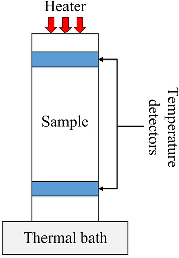
Basic operational principle of the steady-state method is shown in Fig. 1. For measuring the thermal conductivity, we heated one end of the sample with a certain power, while the second one is connected to a thermal bath, measured temperature on both ends of the sample, found constant temperature difference, and calculated thermal conductivity from Eq. (1a).
Principal design of the steady-state method.

This method has some requirements for sample geometry. In our case, we estimated the necessary width of the sample for getting noticeable temperature difference. Sample length was limited by a crystal size (l = 3 mm) and the thickness was small enough (d = 100 µm). In accordance with Eq. (1a), sample width a could be estimated as
 $$a = \displaystyle{P \over {\kappa \cdot \Delta T}}\displaystyle{l \over d},$$
that gives the value of about 0.2 mm. This estimation was made using the expected maximum diamond thermal conductivity of about 15,000 W/(m·K), available heater power 50 mW and the temperature difference of 0.5 K that we can measure with a high accuracy and reproducibility.
Samples preparation
We used synthetic single-crystal diamonds grown by the temperature gradient method under high pressure of 5.5 GPa and high temperature 1440 °C (HPHT) in a “toroid” type high-pressure apparatus. Fe–Al–C alloy (91:5:4 by wt.%) was used as the solvent metal. Aluminum was added to the solvent as a nitrogen getter. High purity (99.9995%) graphite was used as a carbon source.
An amorphous boron powder of 0.5 at% was added to the carbon source for IIb-type diamond growth. The resulted boron content in the grown BDD crystals was about 1019 cm−3 (~20 ppm) according to IR spectra. The electrical properties and growth issues of such doped crystals were described in.[ Reference Bormashov, Tarelkin, Buga, Kuznetsov, Terentiev, Semenov and Blank 16 , Reference Blank, Kuznetsov, Nosukhin, Terentiev and Denisov 17 ]
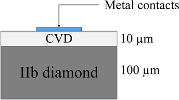
After diamond crystals growth (001) plates were cut from them by laser, and then mechanically polished. The thickness of plates after polishing was about 100 µm. The thin (~10 µm) layer of isolating IIa-type diamond was grown by the chemical vapor deposition (CVD) process on BDD plate for electrical isolation (Fig. 2). Then diamond plates were chemically cleaned in SAS, acetone, isopropanol, and annealed on the air at 680 °C in order to remove any contaminations and avoid surface H-related conductivity (after CVD growth).
Cross-section of the sample after growth of CVD layer.

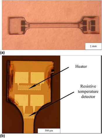
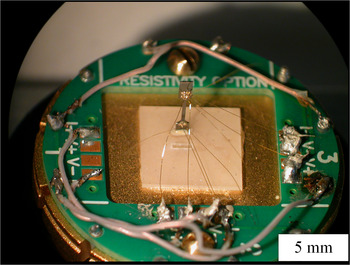
After that three platinum resistors of 1 kΩ resistance have been deposited using lift-off lithography and magnetron sputtering. Two of these resistors were used as temperature detectors for hot and cold sample edges. The last one was used as a resistive heater to provide heat pulse. Finally, the required sample geometry with small cross-section heat conductive neck of 0.3 mm width and 3 mm length was created by laser cutting (Fig. 3). Samples were mounted on a standard PPMS sample puck using special epoxy with high thermal conductivity to provide good thermal contact. This puck provides electrical connections of detectors and the heater and at the same time plays role of a thermal bath. The electrical connections were made using 40-μm thick gold wires (Fig. 4).
(a) Photograph of the sample with temperature detectors and heater, (b) Zoomed photograph of the heater and temperature detector.

Photograph of the sample installed on the sample puck.

Experimental results and analysis
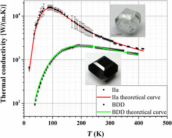
Experimental data on both samples are presented in Fig. 5. As one can see, the thermal conductivity of IIa diamond at room temperature is about 2500 W/(m·K) that is similar to known data.[ Reference Olson, Pohl, Vandersande, Zoltan, Anthony and Banholzer 13 – Reference Wei, Kuo, Thomas, Anthony and Banholzer 15 ] A maximum value of the thermal conductivity was slightly above 17,000 W/(m·K) at 90 K. Below 150 K the thermal conductivity of BDD is roughly ten times less than that of IIa diamond, but at temperatures higher than 300 K the difference is just about 30%.
Experimental data on both pure IIa and BDDs.

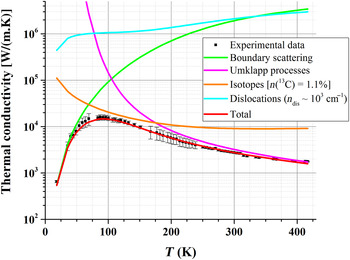
Figure 6 displays the best fit theoretical curve to experimentally measured temperature dependence of thermal conductivity of IIa accounting for different mechanisms of phonon scattering. We calculated the temperature dependence of the thermal conductivity using the best fit within the framework of improved Callaway model.[ Reference Callaway 18 ]
Measured and calculated thermal conductivity of IIa diamond. Influence of different processes of phonon scattering is also illustrated.

Below Debye temperature (≈1900 K for diamond) heat transport in materials with low density of electrical charge carriers is provided by acoustic phonons.[ Reference Kittel 19 ] Thermal resistivity in isolators and semiconductors occurs due to inelastic phonon scattering. We considered different types of inelastic phonon scattering such as phonon–phonon scattering, scattering on point defects (substitutional atoms and isotopes), extended defects (dislocations), and crystal boundaries. Callaway model assumes that different processes of phonon scattering do not interfere on each other and have different specific times τ i . Then the total scattering time τ is given by the relation:
 $$\displaystyle{1 \over {\tau _{\rm c}}} = \sum\limits_i {\displaystyle{1 \over {\tau _i}}}. $$
In this work, we used the following expressions for the scattering time of each process. For normal processes[ Reference Wei, Kuo, Thomas, Anthony and Banholzer 15 ]:
 $$\displaystyle{1 \over {\tau _{\rm N}}} = AT^3 \displaystyle{\omega \over {2\pi}} {\rm,} $$
where A is the temperature-independent parameter, T the temperature, and ω the phonon frequency. For umklapp processes[ Reference Tritt 20 ]:
 $$\displaystyle{1 \over {\tau _{\rm U}}} = Bv\lambda ^{ - 2} T\;\exp \left( { - \displaystyle{C \over T}} \right){\rm,} $$
where B and C are temperature-independent parameters, λ the phonon wave length, and v the average sound velocity in the material. For boundary scattering[ Reference Tritt 20 ]:
 $$\displaystyle{1 \over {\tau _{\rm b}}} = \displaystyle{v \over d}{\rm,} $$
where d is a parameter associated with the sample size.
For point defects we considered isotopic substitution in the same manner as doping[ Reference Tritt 20 ]:
 $$\displaystyle{1 \over {\tau _{\rm P}}} = \left\{ {\displaystyle{{V_0} \over {4\pi v^3}} \omega ^4 \left[ {\left( {\displaystyle{{\delta M} \over M}} \right)^2 + 8n_{\rm P} V_0 \left( {\displaystyle{{\delta R} \over R}} \right)^2} \right]} \right\}^{ - 1} {\rm,} $$
M is the atomic mass of the crystal; δM the difference between masses of substitutional and host atoms; R and δR the radius of the host atom and difference between radiuses of substitutional and host atoms; V 0 the volume per atom; and n p the point defects density. The first term of the equation is responsible for the mass difference of atoms and the second one accounts lattice deformations caused by doping. In a case of isotopic substitution the second term equals to 0.
In a case of scattering of the phonons on extended structural defects, there are two factors to be considered: scattering on lattice defects and scattering on elastic field, caused by the defect. In[ Reference Tritt 20 ] the following expressions for scattering times are given:
 $$\displaystyle{1 \over {\tau _{{\rm core}}}} = K_1 N_{\rm D} \displaystyle{{r^4} \over {v^2}} \omega ^3 {\rm,} $$
 $$\displaystyle{1 \over {\tau _{{\rm str}}}} = K_2 N_{\rm D} \displaystyle{{\gamma ^2 B_{\rm D}^{\rm 2}} \over {2\pi}} \omega {\rm,} $$
where K 1, K 2 are the temperature-independent parameters, N D the dislocation density, B D the Burgers vector of the dislocation, r the dislocation radius, and γ the Gruneisen parameter.
We calculated the temperature dependences of thermal conductivity defined by each particular process (3)–(8) and presented them in Fig. 6. Each curve shows the value of thermal conductivity in a case if there was only one process of phonon scattering. Such a graph illustrates what process of phonon scattering dominates in a certain temperature range. The density of 13C atoms equal to 1.1% was used as the natural abundance in graphite. X-ray diffraction studies show that IIa diamonds grown in TISNCM have very low density of dislocations,[ Reference Shvyd'ko, Stoupin, Blank and Terentyev 4 ] so they should not have any influence on thermal conductivity. Even in a case of upper estimation of the dislocation density of about 103 cm−2 (near different growth sectors boundary) they do not affect thermal conductivity of IIa diamond.
For low temperature the position and the height of the thermal conductivity maximum is determined by two processes: boundary scattering of phonons and scattering on isotope 13C atoms. At T > 200 K umklapp processes limit the thermal conductivity and from 200 to 300 K scattering on 13C isotopes has some weak influence. Fitting this data range with the theoretical model gives us the values of parameters A and B from Eqs. (3) and (4). We used a medium value of the parameter C = 670 K from[ Reference Wei, Kuo, Thomas, Anthony and Banholzer 15 ] as it has weak influence on the final result of calculations. The optimal values of the fitted parameters are given in Table I.
Values of model parameters from literatures and found by best fit in our study.

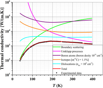
Figure 7 shows the experimental results and theoretical curves for BDD like it was done for IIa type. The theoretical curve fits well the experimental data in a whole temperature range. The thermal conductivity of such IIb diamond has the maximum value of 2100 W/(m·K) at about 190 K that is much less than the value for pure diamond. However, BDD has the relatively high thermal conductivity of 1600 W/(m·K) at room temperature and the difference with IIa diamond becomes less than 30% at the temperature increase.
Measured and calculated thermal conductivity of BDD diamond. Influence of different processes of phonon scattering is also illustrated.

In the case of BDD, we accounted an additional process of phonon scattering on substitutional boron atoms with the density of 1019 cm−3 using Eq. (6). The density of dislocations 106 cm−2 primarily was accounted from the X-ray diffraction topography and gave a good fit within the framework of Callaway model. We used the values of parameters A, B, and C the same as found for IIa diamond (see Table I).
In accordance with our results at T > 300 K, umklapp processes have dominating influence on the thermal conductivity of BDD similarly to the case of IIa diamond. However, the maximum of thermal conductivity of BDD is limited by the scattering on dislocations instead of isotopic impurities. We should emphasize that the thermal conductivity of doped diamond is almost not affected by single substututional boron atoms in a whole temperature range. However, an increase of doping level results in extended structural defects appearance in BDD due to lattice strain relaxation.
Below 100 K a ballistic transport of phonons is assumed. This means that parameter d in (5) equals to phonon-free path length. A good fit was found at d ≈ 10 µm. We may assume an occurrence of extended defects in heavily BDD similar to crystal boundaries that limit the phonon-free path.
Conclusions
We performed comparative studies of thermal conductivity of single-crystal high-quality pure IIa-type and BDDs in the temperature range from 20 to 400 K. We found that above room temperature phonon–phonon scattering have dominating influence on the thermal conductivity for both the crystals. Thus, the difference between thermal conductivities of the studied IIa- and IIb-type diamonds at T > 300 K is <30%. These data should be accounted at design of diamond electronic devices operating at high temperatures.
However, the maximum of thermal conductivity of BDD at low temperature is limited by the scattering on structure defects instead of isotopic impurities in a case of IIa diamond. That results in a sharp decrease of thermal conductivity in BDD with respect to IIa diamond at T < 140 K. According to data analysis at this temperature region, phonon scattering on extended structure defects has stronger effect on thermal conductivity of BDD than the scattering on substitutional boron atoms.
The value of thermal conductivity of BDD at T < 100 K calculated using “classical” boundary scattering time is higher than the experimentally found value. We suppose that some additional extended structure defects limit the phonon-free path up to about 10 µm. Thermal and structure investigations of single-crystal diamonds with different boron content should be carried out to study this effect in detail.
Acknowledgments
Thermal conductivity measurements were carried out using the facility of the Shared-Use Equipment Center of the Technological Institute for Superhard and Novel Carbon Materials. The work at TISNCM was supported by the Ministry of Education and Science of the Russian Federation, scientific project no.14.580.21.0003 (RFMEFI58015X0003).