I. SPINTRONICS AND MAGNETORESISTIVE RANDOM ACCESS MEMORIES
The term “spintronics” refers to the branch of physics concerned with the manipulation, storage, and transfer of information by means of electron spins in addition to or in place of the electron charge as in conventional electronics. Reference Wolf, Awschalom, Buhrman, Daughton, von Molnár, Roukes, Chtchelkanova and Treger3 Spintronics has inherent merits including very low power dissipation, nonvolatility, and the possibility of integrating memory and logic into a single device.
Major advances in electron spin transport started in the late 1970s and 1980 with the discovery of large low temperature magnetoresistance in metallic superlattices. Reference Baibich, Broto, Fert, Van Dau, Petroff, Etienne, Creuzet, Friederich and Chazelas4,Reference Schuller, Falco, Hilliard, Ketterson, Thaler, Lacoe and Dee5 Later, giant magnetoresistance (GMR) at room temperature (RT) was discovered in 1988 in metallic thin film multilayer structures with alternating ferromagnetic (Fe) and nonmagnetic (Cr) layers, which became a device called a “spin valve”. The discovery of the GMR effect won Drs Albert Fert and Peter Grünberg the Nobel Prize in Physics in 2007. Reference Fullerton and Schuller6
Later demonstrations of the ‘giant’ effect at RT evolved toward applications to practical devices. Reference Prinz7 Spin valves exhibit significant changes in resistivity when subjected to relatively small external magnetic fields. Thus, they can be used as magnetic field sensors as in the read head in the hard disk drive (HDD). The first GMR-based magnetic field sensor was created in 1994, and high-performance disk drives utilizing GMR-based read heads to detect magnetic fields were realized in 1997 and now are ubiquitous. These read heads are responsible for the very rapid growth in magnetic storage densities.
Spin dependent tunneling was first discovered by Tedrow and Meservey in a series of experiments in ferromagnet/insulator/superconductor (F/I/S) junctions. Reference Tedrow and Meservey8,Reference Tedrow and Meservey9 These experiments showed that conduction electrons in ferromagnetic (FM) materials are spin polarized and the spin is conserved during the tunneling process.
In 1975, Julliere studied the tunneling conductance of ferromagnet/insulator/ferromagnet (F/I/F) where the insulator was an amorphous Ge layer. Reference Julliere10 By applying the same analysis of the tunneling conductance of F/I/S from Tedrow and Meservey to F/I/F, he formulated a model to describe the change of conductance between the parallel (P) and antiparallel (AP) magnetization of the two FM layers. The corresponding tunneling magnetoresistance (TMR) in a F/I/F type structure, called magnetic tunnel junction (MTJ), is defined as Reference Julliere10
 $${\rm{TMR}} = {{\Delta R} \over {{R_{\rm{P}}}}} = {{{R_{{\rm{AP}}}} - {R_{\rm{P}}}} \over {{R_{\rm{P}}}}}\quad ,$$
where the resistances (R) are labeled by the relative orientation (P or AP) of the magnetizations of F1 and F2.
The achievement of RT TMR in 1995 attracted a great deal of interest from research groups across the world, Reference Moodera, Kinder, Wong and Meservey11,Reference Miyazaki and Tezuka12 mainly due to the huge potential industrial applications of TMR and the broader research field by exploring another degree of freedom, the spin of the electron, besides the conventional manipulation of the electron charge.
The initial breakthrough on MTJs with simple electrodes like CoFe and Fe produced TMR just over 10%. Materials-wise, by replacing polycrystalline electrodes like CoFe and NiCoFe with amorphous CoFeB and optimizing the growth conditions, a record high MR value of 70% was achieved on MTJs with aluminum oxide barriers. Reference Wang, Nordman, Daughton, Qian and Fink13 The breakthrough came after first principle calculations predicted that MTJs with epitaxial Fe/MgO/Fe structure could provide significant spin filtering that would enhance the MR to over 1000% Reference Butler, Zhang, Schulthess and MacLaren14 and was soon demonstrated experimentally with TMR around 200% by two different groups independently. Reference Parkin, Kaiser, Panchula, Rice, Hughes, Samant and Yang15,Reference Yuasa, Nagahama, Fukushima, Suzuki and Ando16 By optimizing the composition of CoFeB, recently TMR ratios of up to 500% have been achieved at RT in CoFeB/MgO/CoFeB MTJs. Reference Lee, Hayakawa, Ikeda, Matsukura and Ohno17 All of these efforts have greatly enhanced the potential of MTJs in spintronic device applications like data storage, magnetic sensors, etc.
Besides the improvement of materials for making better MTJs, different layered structures have also been intensively studied to produce MTJs more suitable for practical applications. The initial MTJs have the simplest structure of two FM layers sandwiched by an ultrathin insulating barrier layer. One of the FM layers has relatively large magnetic anisotropy and its magnetization direction is fixed as the reference orientation, so this FM layer is called reference layer (RL). The other FM layer, called the free layer (FL), has relatively low coercivity and hence its magnetization can be flipped in one of the two directions easily to achieve the relative high and low resistance of the whole MTJ stack.
To achieve a more stable RL, the exchange bias (EB) mechanism was utilized by adding an antiferromagnetic layer (AFM) next to the FM RL to form the bilayer EB system. Reference Nogués and Schuller18 Basically, due to the EB coupling between the FM/AFM layers, the hysteresis loop of the EB system will be shifted off center along the field direction caused by the EB anisotropy. By shifting the hysteresis loop of the RL, a more stable and wider range of separation of the two FM layers was achieved. To reduce the magnetic stray field from the RL and further stabilize the RL, the FM layer in the EB system was replaced by a trilayer system with two FM layers sandwiching a nonmagnetic metal layer through which the FM layers are coupled antiferromagnetically.
MRAM is based on the concept of using the direction of magnetization to store information, and magnetoresistance (variation in resistance with magnetization) as information readout. Reference Wolf, Jiwei, Stan, Chen and Treger19 It was originally invented in the late 1980s to replace bulky and heavy plated wire radiation hard memories. MRAM was a truly nonvolatile (i.e., retains memory when power is off) memory device for specialty radiation hard applications when it was first invented, with dimensions larger than 1 μm. Large TMR in MTJ materials enabled, Reference Parkin, Kaiser, Panchula, Rice, Hughes, Samant and Yang15,Reference Yuasa, Nagahama, Fukushima, Suzuki and Ando16 for the first time, one MTJ element and one transistor bit cell (1 TMTJ) architecture.
A MRAM chip product prototype using toggle magnetic field switching scheme was announced in 2003 and the first ever MRAM commercial products started to ship in 2006. Reference Engel, Akerman, Butcher, Dave, DeHerrera, Durlam, Grynkewich, Janesky, Pietambaram, Rizzo, Slaughter, Smith, Sun and Tehrani20 The manufacturability of MTJ devices as memory bits was proven in these nonvolatile MRAM products, having high read and write speeds (10s of ns) and nearly unlimited endurance.
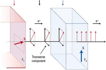
Spin torque transfer (STT)-MTJ utilizes a spin polarized current to directly switch the magnetization of a nanomagnet. It was theoretically predicted in 1996, which was based on a generally accepted argument: For a system consisting of itinerant electrons and local moments, the total angular momentum is conserved even when the system is out of equilibrium. Reference Slonczewski21,Reference Berger22 The STT mechanism is illustrated in Fig. 1 within a spin valve or MTJ structure frame. Reference Chappert, Fert and Van Dau23
STT in ferromagnetic metal (FM)/normal metal (NM)/ferromagnetic metal (FM) structures. The red layer is the fixed layer while the blue layer represents the FL. Electrons become spin polarized when they flow through the FM fixed layer (F1). The spin polarized current exerts a spin torque (the transverse component) on the magnetic moment of the FL (F2) due to the interaction between the electron spin and local magnetization [adapted from Ref. Reference Chappert, Fert and Van Dau23].

Compared to the use of external fields generated by passing current in conventional toggle switch scheme, the STT switching scheme has a desirable scaling behavior, namely, it is the current density rather than the absolute current that is important, so the actual current scales down properly with the device size. The theoretical expression of this critical current density J c0 required to switch the magnetization of a ferromagnet with an in-plane magnetic anisotropy is predicted by Slonczewski Reference Slonczewski21 :
 $${J_{{\rm{c}}0}} = {{2e\alpha {M_{\rm{s}}}{t_{\rm{F}}}\left( {H_{\rm{K}}}\, \pm\, {H_{\rm{ext}}} + 2\pi {M_{\rm{s}}}} \right)} \over {\hbar\eta }}\quad ,$$
where e is the charge on an electron, α is the Landau–Lifshitz–Gilbert damping parameter, M s is the saturation magnetization, t F is the thickness of the FL, H is the applied magnetic field, H K is the effective uniaxial anisotropy field of the FL, η is the spin transfer efficiency, and h is Planck's constant, respectively. The sign denotes the positive and negative direction of the electron current flow, with the positive direction defined as electrons flowing from the fixed RL to the FL.
STT was first demonstrated in metallic spin valve thin films with critical switching current density (J c0) > 107–108 A/cm2, which is too high for practical memory devices. Reference Sun, Monsma, Abraham, Rooks and Koch24,Reference Pufall, Rippard and Silva25 In order for this current drive STT switching to be viable in the MRAM architecture, the critical current density needs to be reduced to the level ∼105 A/cm2. Reference Chen, Apalkov, Diao, Driskill-Smith, Druist, Lottis, Nikitin, Tang, Watts, Wang, Wolf, Ghosh, Lu, Poon, Stan, Butler, Gupta, Mewes, Mewes and Visscher26 Perpendicular MTJs (PMTJ) for STT-RAM have been investigated to solve this problem, and indeed very low STT writing current was demonstrated at reasonably high thermal stability. Reference Kishi, Yoda, Kai, Nagase, Kitagawa, Yoshikawa, Nishiyama, Daibou, Nagamine, Amano, Takahashi, Nakayama, Shimomura, Aikawa, Ikegawa, Yuasa, Yakushiji, Kubota, Fukushima, Oogane, Miyazaki and Ando27,Reference Zhu and Zhu28 Perpendicular magnetic materials have been extensively studied for HDD application as a recording medium. This type of material is capable of having a very high magnetic anisotropy field arising from the atomic properties of these materials. No shape anisotropy is required, and circular shaped bits can be used, which simplifies the manufacturing process. Sizes below even 10 nm are expected to have enough thermal stability due to the high anisotropy field (>2 Tesla) in some of these materials. The main challenges of making PMTJ work for STT-RAM are how to make these materials compatible with the MgO tunnel barrier, yielding high TMR ratio and spin transfer efficiency, while also having lower damping constants to have lower STT writing currents.
II. RADIATION DAMAGE TO ELECTRONIC DEVICES
Radiation environments vary significantly in their range of particle types and energies. In outer space, damage arises mainly from trapped electrons and protons having energies up to about 100 MeV. 29 Earth's geomagnetic field interacts with protons and electrons from the solar wind to form the van Allen radiation belts. From altitudes between about 1300 and 60,000 km, satellites and other space-bound objects are bombarded with trapped protons and electrons that can have energies in excess of 10 MeV. The resulting damage to materials, devices, and systems largely takes the form of displacement and ionization damage.
Displacement damage is the result of atoms being moved from their original positions. Reference Weaver and Summers30 Unlike ionization damage, it affects conductors and insulators alike. For relatively small particle fluences (Φ), the induced defect concentration, c, can be written as Reference Weaver and Summers30
 $$c = \Phi A\left( {{\rm{NIEL}}} \right)\quad ,$$
where NIEL is the nonionizing energy loss (the density-normalized rate at which an incident particle loses energy to displacements), Reference Jun, Xapsos, Messenger, Burke, Walters, Summers and Jordan31 and the parameter A depends in part on the fraction of atoms that do not recombine immediately following irradiation. The units of c are typically “displacements per target-material atom,” or dpa. Because the value of A is generally unknown, one frequently defines the displacement damage dose D as D = Ф × NIEL and uses it as a parameter known to be directly proportional to c.
Ionization damage is characterized by trapped charge. When an energetic particle passes through an insulator or a poor conductor, it transfers energy to the local electron cloud, which causes carriers to be excited into conduction states. Most carriers recombine as the excess energy dissipates and the material returns to its poor conducting state, but some remain behind as trapped charge. The resulting ionization damage introduces localized electric fields, shifts threshold voltages, and increases noise.
A great deal has been learned about the transport properties of electronic devices by observing how various operating parameters such as the drain and gate currents change with changing displacement damage dose. On the other hand, very little is known about the effect of induced disorder on electron spin and spin currents. In fact, there is a tradition among radiation-effects scientists of ignoring the topic. In “Imperfections in Nearly Perfect Crystals” published in 1952, Reference Shockley, Hollomon, Maurer and Seitz32 Seitz wrote: “Ferromagnetic and ferroelectric solids can contain imperfections in the form of spin disorder but in the interest of simplicity, we shall omit such topics from detailed consideration…”. Since then, there is an absence of systematic studies and comprehension on the disorder effects in magnetic materials related to spintronic devices despite of “Rad Hard” MRAM technology. 1,Reference Gerardin and Paccagnella2,Reference Katti, Lintz, Sundstrom, Marques, Scoppettuolo and Martin33
III. EFFECTS OF IRRADIATION ON MTJs
The effect of heavy ion irradiation on the magnetotransport properties of MTJs has been investigated but mostly on MTJs with Al2O3 barriers. Reference Banerjee, Som, Kanjilal and Moodera34–Reference Schmalhorst and Reiss39 Many studies focus on either the magnetic properties or the magnetotransport properties of MTJs in postirradiation characterizations, and few have done careful comparison on the evolution of the microstructure, particularly the interfaces during the irradiation process. The critical performance metrics for MTJ is the TMR. The change in the TMR in postirradiation MTJs varied greatly in accordance with the radiation species/energy/dosage.
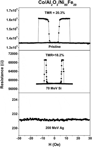
Moodera and his collaborators Reference Banerjee, Som, Kanjilal and Moodera34 studied two types of tunnel junctions, viz. Co/Al2O3/Ni80Fe20 and Co/Gd-doped Al2O3/Ni80Fe20 with two types of heavy ion irradiations, namely, 70 MeV Si ion irradiation at a fluence of 5 × 10¹¹ ions/cm2 and 200 MeV Ag at a fluence of 1 × 10¹¹ ions/cm2. The change in the TMR is shown in Fig. 2. Upon irradiation, the TMR of the undoped junctions showed relatively small but irreversible change (from ∼20 to ∼18%), while as that of a doped junction showed large change, reducing from ∼18 to ∼0.3%. One could speculate that the Gd-doped Al2O3 is metastable, in which case the MTJ breakdown would be expected. The TMRs became negligible after the 200 MeV Ag ion irradiation at a very low fluence of 1 × 10¹¹ ions/cm2, as seen in Fig. 2. Through stopping and range of ions in matter simulation, the Ag ion was predicted to cause severe displacement damage to the Co and Al2O3 layers. In particular, it appears that the recoil implantation occurred in the Gd-doped MTJ that results in large rearrangements of chemical species. It is worth noting that there are no detailed characterizations of the chemical distribution and the microstructure, particularly the roughness of the interfaces in these junctions prior and postirradiation.
TMR versus H field for Co/Al2O3/Ni80Fe20 MTJs irradiated by 70 MeV Si and 200 MeV Ag [adapted from Ref. Reference Banerjee, Som, Kanjilal and Moodera34].

In an attempt to elucidate the effect of the damage to the Al2O3 barrier layer, low energy He+ and Ar+ ions with energies from 15 to 105 eV were used to irradiate the barrier layer in situ by Sacher et al. Reference Sacher, Sauerwald, Schmalhorst and Reiss37 As a result of low energy ion irradiation, the resistance of the junctions increases with ion energy, and the TMR is reduced. However, a clear discrepancy in the ion energy dependence of the TMR and resistivity was observed by He+ and Ar+. The different masses of the ions, different energy loss per unit depth, and different ion fluence impact the lower barrier interfaces between the barrier layer and the FM layer differently. For instance, Ar ions nearly all stop in the barrier layer due to the large energy loss per unit depth, thus a relative low ion energy results in the rapid deterioration of the spin dependent tunneling. In contrast, much higher ion energy is required for He+ ions to penetrate the thickness of the barrier layer to cause a pronounced degradation in the TMR value.
Other efforts have been focused on the manifestations of the interlayer recoil and intermixing through the magnetic properties, particularly the interlayer magnetic couplings in MTJs. Qi et al. Reference Qi, Wang, Yan, Miao and Li38 reported degradations in both the magnetization of the FL and the EB field (H ex) simultaneously in IrMn/CoFe/AlO x /CoFe MTJs that were irradiated by Ga+ ions with the energy of 30 keV and the fluence up to 3 × 10¹⁴ ions/cm2. In a separate report, Reference Snoeck, Baules, BenAssayag, Tiusan, Greullet, Hehn and Schuhl40 the two step hysteresis loop in MTJs, which is due to the separated magnetization reversal processes for the FL and the fixed layer, became one regular hysteresis loop observed as a result of 150 keV N+ irradiation at the fluence of 3 × 10¹⁶ ions/cm2. The evaluation is attributed the strong FM coupling between the free and fixed layers caused by the interface roughening.
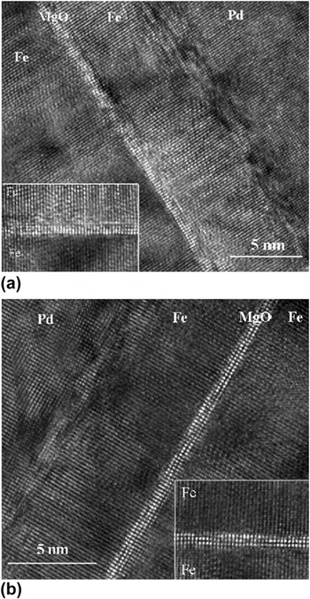
Many of these observed changes in the magnetotransport and the magnetic properties of MTJs were attributed to intermixing among layers; however, only a few had done careful microstructural characterization such as cross-section transmission electron microscopy (TEM) to confirm it. The application of TEM can give a direct insight into the roughening of the interfaces as shown in Fig. 3, Reference Snoeck, Baules, BenAssayag, Tiusan, Greullet, Hehn and Schuhl40 but it is difficult to quantify the change in the intermixing/roughness due to the limited sampling areas. Atomic force microscopy was also used to characterize the change in the surface roughness. Reference Qi, Wang, Yan, Miao and Li38 The surface roughness can be used to infer the intermixing in the MTJ structures, but still cannot quantify the intermixing at the buried interfaces.
High resolution TEM images of Pd/Fe/MgO/Fe junctions irradiated by 150 keV N+ at the fluence of (a) 5 × 10¹⁵ ions/cm2 and (b) 3 × 10¹⁶ ions/cm2 [adapted from Ref. Reference Snoeck, Baules, BenAssayag, Tiusan, Greullet, Hehn and Schuhl40].

X-ray reflectivity (XRR) utilizes the interference of x-ray beams reflected by the different interfaces to create a reflectometry pattern that provides important information about the film thickness. Reference Gibaud and Hazra41 For an incident angle below a critical angle, the incident x-ray beam is totally reflected by the sample surface. The critical angle is related to the refractive index of a material, which depends on the material's electron density. Generally, the critical angles for most materials are less than 1°. As the incident angle gradually increases beyond the critical angle, the incident x-ray beam penetrates into the material and the reflection from the different interfaces of the sample gives rise to interference fringes also known as Kiessig fringes. The amplitude of the fringes depends on the difference in electron density at the interfaces as larger difference leads to higher amplitude. Also, the reflected intensity decays more rapidly with increasing roughness at the surface and interface due to the diffuse scattering. Reference Bowen and Tanner42 The film thickness t can be estimated from the periodicity of the fringes:
 $$t \approx {\lambda \mathord{\left/ {\vphantom {\lambda {\Delta 2\theta }}} \right. \kern-\nulldelimiterspace} {\Delta 2\theta }}\quad ,$$
where λ is the x-ray wave length and Δ2θ is the 2θ angular separation between consecutive interference peaks. Reference Brower, Revay and Huang43
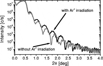
Figure 4 illustrates the change in XRR results for the same Co/AlO x /Co structure with the AlO x barrier with and without the exposure of the Ar+ ion irradiation. One can extract the information on the density and the thickness, as well as the surface/interface roughness via the simulation. In turn, the intermixing of individual layers can be quantified by the changes in the thickness, the density, and the roughness of each layer. Reference Schmalhorst and Reiss39,Reference Snoeck, Baules, BenAssayag, Tiusan, Greullet, Hehn and Schuhl40
XRR of Co/AlO x /Co multilayers with and without 150 eV Ar+ irradiation [adapted from Ref. Reference Schmalhorst and Reiss39].

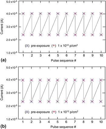
Recent efforts have been focused on the STT-MTJs with MgO barrier layer, Reference Hughes, Bussmann, McMarr, Shu-Fan, Shull, Chen, Schafer, Mewes, Ong, Chen, Mendenhall and Reed44–Reference Kobayashi, Kakehashi, Hirose, Onoda, Makino, Ohshima, Ikeda, Yamanouchi, Sato, Enobio, Endoh and Ohno46 in which the FL and the fixed layer are typically amorphous CoFeB. Hughes et al. Reference Hughes, Bussmann, McMarr, Shu-Fan, Shull, Chen, Schafer, Mewes, Ong, Chen, Mendenhall and Reed44 first investigated the spin torque switching and the state retention of MTJ devices provided by Grandis Inc. The MTJ devices were irradiated by proton ions with energy up to 220 MeV and fluences up to 1 × 10¹² ions/cm2. The switching behaviors of these STT-MTJs were identical before and after proton exposure as shown in Fig. 5. Also no effects were observed on the state retention. Most recently, Kobayashi et al. Reference Kobayashi, Kakehashi, Hirose, Onoda, Makino, Ohshima, Ikeda, Yamanouchi, Sato, Enobio, Endoh and Ohno46 reported that the heavy ion irradiation (15 MeV Si ions) caused a very small degradation (∼1%) in resistance, but no significant changes in the retention state and time before and after irradiation.
Spin torque switching of MTJ before and after (a) 2 MeV proton exposure and (b) 220 MeV proton exposure. For both sources, the fluence is 1 × 10¹² ions/cm2 [adapted from Ref. Reference Hughes, Bussmann, McMarr, Shu-Fan, Shull, Chen, Schafer, Mewes, Ong, Chen, Mendenhall and Reed44].

There are very few radiation studies that focus on the ionization damage to the MgO oxide barriers (which are typically 1 nm thick in STT-MTJs). Hughes et al. Reference Hughes, Bussmann, McMarr, Shu-Fan, Shull, Chen, Schafer, Mewes, Ong, Chen, Mendenhall and Reed44 exposed MTJ with a 1.2 nm MgO barrier to Co60 γ-rays with doses up to 10 Mrad (Si) and did not observe any change in TMR, resistance area product (RA) values as well as the spin torque switching behaviors.
IV. EFFECTS OF ION IRRADIATION ON MAGNETIC MATERIALS
Electron, neutron, proton, alpha particle, and gamma rays are the common sources of radiation from space and onboard nuclear reactors. Upon interacting with matter, the kinetic energy transferred from the high-energy particle to the atomic nucleus is often sufficient to break the chemical bonds to neighboring atoms. The liberated atom serves as a secondary energetic particle to produce other atomic displacements, excitations, or both, along its path. In solids, the collision cascades often lead to heat spikes and the formation of defect clusters as well as various randomization phenomena.
In recent years, ion irradiation has been widely applied to modify magnetic properties in thin films or superlattices. Reference Chappert, Bernas, Ferré, Kottler, Jamet, Chen, Cambril, Devolder, Rousseaux, Mathet and Launois47–Reference Esquinazi, Spemann, Hohne, Setzer, Han and Butz51 The response to radiation varies among materials and cannot be predicted in general. Prior experiments on amorphous, crystalline, and nanocrystalline materials have revealed effects ranging from defect formation, structural disorder, structural relaxation, crystallization, and phase separation. The effects on magnetic properties apparently are found to depend on the type of radiation, particle energy and fluence, alloy composition and structure, and degree of inherent structural order and disorder, as well as material system size. In general, irradiation has slower effects on amorphous alloys than crystalline alloys. Reference Brown, Cost and Stanley52 Earlier studies of radiation effects on magnetic materials and tunnel-junction devices are summarized below.
A. Amorphous alloys
Irradiation with protons, electrons, and alpha particles produces structural relaxation in some amorphous iron-based alloys. Reference Fisher53 Deterioration of the soft magnetic properties due to neutron irradiation occurs predominantly in the higher fluence range (1018–1019 neutrons/cm2). Opposing effects on the magnetic permeability of magnetic metglass and Mumetal occur at different stages. Excess point defects produced by neutron irradiation enhance the short-range ordering, but defect clusters produced in the collision cascades in the heat spike regime cause the pinning of domain walls. Induced stress due to irradiation can also affect the magnetic anisotropy. For example, in magnetic steel Reference Park, Kim, Kim, Hong and Kim54 and metglass, Reference Kim, Yu, Kim, Han, Cho and Kim55 the coercive force increased after neutron irradiation at 1016 n/cm2 dose compared with that of the unirradiated one, related to the domain wall motion hindered by the increased defects.
B. Nanomaterials
Studies have shown that materials with high radiation resistance can be designed by changing the composition, crystal size, and degree of inherent disordering. Reference Zhang, Lian, Fuentes, Zhang, Lang, Lu and Ewing56,Reference Zhang, Lian, Zhang, Wang, Fuentes and Ewing57 Defect generation and interaction in nanoscale systems often lead to unusual physical properties. Earlier experiments found that the deterioration of magnetic properties due to particle irradiation is less significant in Fe-based nanocrystalline alloys compared with their crystalline counterparts. Reference Skorvanek, Gerling, Graf, Fricke and Hesse58 Other studies have revealed a strong correlation between defect density and grain/particle size in nanostructured bulk materials Reference Rose, Balogh and Hahn59 and nanoparticles. Reference Narayan60 As the grain/particle size decreases to about 10–30 nm, below the mean distance between defects, the material can become defect free in equilibrium. However, nonequilibrium defects can be introduced by processing, internal stresses, and particle irradiation. Thus, it is interesting to note that small ZrO2 (<15 nm) and Pd (<30 nm) grains can remain defect free upon irradiation by 4 MeV Kr+ ions with fluences up to 2 × 10¹⁶ Kr+/cm2. More recently, a greatly enhanced resistance to radiation-induced amorphization was observed in nanocrystalline magnetic oxides, e.g., pyrochlores, at a particle size less than 20 nm. These results indicate exciting research opportunities on the effect of radiation in nanomagnetic films, particularly in regard to the design of radiation-hard magnetic devices.
Characterization of magnetic Ni–Fe thin film Reference Kuwahara, Yamamoto and Kobayash61,Reference Fassbender and McCord62 and Fe–Tb and Pt/Co/Pt multilayers Reference Gupta, Paul, Gupta, Avasthi and Principi63,Reference Blon, Chassaing, Ben Assayag, Hrabovsky, Bobo, Ousset and Snoeck64 upon irradiation has revealed interfacial roughening and interlayer mixing as well as stress relaxation of the growth texture. Deuteron, nitrogen ion, and other heavier ions with particle energy in the range 30 keV to 150 MeV and fluence in the range 1015–1016 ions/cm2 were used in the experiments. The magnetic anisotropy was found to be reduced, and a strong enhancement of the magnetic damping parameter was also reported. For the Ni–Fe film, the uniaxial anisotropy direction could be set by ion implantation in an applied magnetic field, irrespective of its original orientation.
C. Crystalline alloys
For crystalline materials, the effects of high-energy particle and gamma irradiation depend on many factors such as: (i) The material's proneness to disorder, amorphization, or swelling, which depends on the crystal structure. Amorphization resistance was found in compounds that have a natural tendency to accommodate lattice disorder due to neutron and heavy-ion irradiation, e.g., oxides with the structures related to the fluorite crystal structure. Reference Sickafus, Grimes, Valdez, Cleave, Tang, Ishimaru, Corish, Stanek and Uberuaga65 (ii) High-energy heavy-ion irradiation can result in lattice expansion and diffusion-enhanced phase separation. For example, both large increases and small decreases of the Curie temperature have been observed in Fe–Ni, Fe–Pd, and Fe–Pt Invar alloys irradiated by 200 MeV Xe-ions to the fluence of 1014 ions/cm2, attributed to lattice distortion and compositional change due to phase separation. Reference Ono, Kanamitsu, Matsushima, Chimi, Ishikawa, Kambara and Iwase66,Reference Ono, Chimi, Ishikawa, Kanamitsu, Matsushima, Iwase and Kambara67 (iii) The thermal stability of the material's intrinsic magnetization and coercivity at temperatures below its Curie temperature could be the key factor in determining the material's resistance to radiation, regardless of the source, i.e., gamma, electron, proton or neutron. Radiation damage is found to be caused by a thermal spike instead of microstructure changes.
D. Chemically ordered magnetic intermetallics
Permanent ferromagnets with the L10 structure that can also be illustrated as a tetragonally distorted B2 ordered structure have been of great interest for ultra-high density magnetic recording media due to their large magnetocrystalline anisotropy (>107 erg/cc). These alloys are very different from the Co-based hexagonal close-packed alloys utilized for the last two decades or so, in that they are tetragonal in symmetry and are atomically ordered structures.
It has been shown that He ion irradiation can induce the chemical ordering of the L10 phase in FePt films, Reference Ravelosona, Chappert, Mathet and Bernas48,Reference Lai, Yang and Chiang50 for which the irradiation induced ordering likely takes place in the vicinity of an ordered crystal structure. It has been suggested that the heating of large beam current acted as a rapid thermal anneal to assist the crystallization of FePt, Reference Lai, Yang and Chiang50 which certainly is advantageous for enhancing the chemical ordering and the coercivity in L10 FePt films.
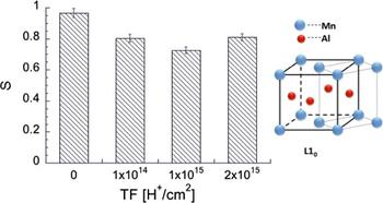
Lu and his collaborators Reference Anuniwat, Cui, Wolf, Lu and Weaver68 have investigated the effect of proton irradiation on τ phase MnAl which is a meta-stable phase with L10 structure, Reference Yanar, Wiezorek, Radmilovic and Soffa69 MnAl has a high saturation magnetization of 490 emu/cc and a large uniaxial magnetocrystalline anisotropy around 107 erg/cc. Reference Koch, Hokkeling, Steeg and de Vos70 Within the B2 unit cell, Mn atoms are located at the corner sites while Al atoms occupy the center sites. Thus, the whole crystal is equivalent to alternating Al and Mn planes along the tetragonal c-axis that can be parameterized by the chemical ordering parameter S. Reference Sands, Harbison, Leadbeater, Allen, Hull, Ramesh and Keramidas71 A high S parameter is required for the perpendicular magnetic anisotropy (PMA) in τ phase MnAl. Reference Yanar, Wiezorek, Radmilovic and Soffa69 The S value of the pre-irradiation sample was ∼0.97, indicating a very high chemical ordering for MnAl films as the result of postdeposition annealing. S was reduced to as low as ∼0.72 when the fluence was increased to 1 × 10¹⁵/cm2. After the third irradiation, the change in the chemical ordering was reversed and S became ∼0.81 as seen in Fig. 6. It implies that with the increase in the fluence to 2 × 10¹⁵ H+/cm2, the effect of displacement damage was overwhelmed by a partial recovery of the chemical ordering. It is worth noting that the saturation moment after the last irradiation became larger than that of the virgin sample. The fact that total magnetization exceeds its original value cannot be explained solely by chemical ordering, implying that there were additional contributions of magnetic moments from the changes in the microstructure in L10 MnAl.
Chemical ordering as a function of total fluence of 2 MeV protons for a 30 nm thick MnAl film. The L10 structure of MnAl is also shown [adapted from Ref. Reference Anuniwat, Cui, Wolf, Lu and Weaver68].

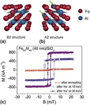
An opposite example for the chemically ordered alloy is Fe60Al40, for which the ordered phase is nonferromagnetic whereas the disordered, body-centered cubic A2 phase is FM as illustrated in Fig. 7. Reference Zamora, Perez Alcazar, Velez, Betancur, Marco, Romero, Martinez, Palomares and Gonzalez73–Reference Trautvetter, Wiedwald, Paul, Minkow and Ziemann75 The magnetization can be induced by 10 and 30 keV Ne+ ions, and the magnitude of the magnetization is controlled by the amount of disordering introduced by the ion bombardment as seen in Fig. 7(c). Reference Bali, Wintz, Meutzner, Hubner, Boucher, Unal, Valencia, Neudert, Potzger, Bauch, Kronast, Facsko, Lindner and Fassbender72
(a) Paramagnetic B2 phase and (b) FM A2 phase of FeAl. (c) Hysteresis loops of FeAl alloys pre- and postirradiation of 10 and 30 keV Ne+ ions. The fluence is 6 × 10¹⁴ ions/cm2 [adapted from Ref. Reference Bali, Wintz, Meutzner, Hubner, Boucher, Unal, Valencia, Neudert, Potzger, Bauch, Kronast, Facsko, Lindner and Fassbender72].

V. CONCLUSION AND OUTLOOKS
As the key element for the MRAM technology, the MTJs have been studied for their resistance to the irradiation damages. It is found that high fluence heavy-ion exposure usually causes the most displacement damage effects in magnetic structures. The interfaces in the MTJs usually are more sensitive to the structural modifications induced by heavy ions. Typically, the magnetic and magnetotransport properties deteriorate as the fluence increases. Cross-section TEM and x-ray reflectivity are the available tools to examine the intermixing between adjacent layers. In contrast, high energy protons and Co60 γ-ray irradiation appear to have very little effects on magnetic properties of MTJs and their STT switching behaviors, which makes MTJs a promising candidate for “Rad Hard” applications in these environments.
Advances in the magnetic nanostructures and new materials for the scalability of STT-MRAM and other potential applications require a re-evaluation of their radiation hardness. In particular, the thickness of the MgO barriers was reduced in the STT-MTJ. Also new magnetic materials with strong perpendicular magnetic anisotropy begin to replace the conventional CoFeB, and some of new materials rely on the interfacial anisotropy in the superlattice structure. There are very few radiation studies that focus on the ionization damage to the MgO oxide barriers that are typically 1–2 nm thick in STT-MTJ. These advances in STT-MTJ technology make the structures more vulnerable to both the displacement- and ionization damage.
The response to radiation varies among magnetic materials and cannot be predicted in general. The effects on magnetic properties apparently are found to depend on the type of radiation, particle energy and fluence, alloy composition and structure, and degree of inherent structural order and disorder, as well as material system size. Irradiation has slower effects on amorphous alloys than crystalline alloys. Particularly for chemically ordered alloys, the magnetic properties are strongly correlated with the chemical ordering. Thus, the modification of the magnetic properties can be very pronounced, thanks to the displacement damages caused by the heavy ion beams. However, the thermal spike associated with the ion irradiation counters the effect of the displacement damages and helps recovering the chemical ordering at the high ion fluence.
ACKNOWLEDGMENTS
J.W. L, S.J. P, B.D. W and E.C. are grateful to the support from the Defense Threat Reduction Agency (Grant No. HDTRA1-11-1-0024). J.W. L and S.A. W. are supported in part by the National Science Foundation (Award number: ECCS-1344218).