Introduction
In modern detection and communication applications, phased array could expand system functionality rather than single-channel front ends. For the considerations of size requirements and package weights, it is recommended to adopt integrated circuits to realize phased array blocks.
For radio frequency variable gain amplifier (RF VGA) block in phased array, amplitude tuning using bias control has been adopted [Reference Wang, Chen, Wu and Wang1–Reference Tessmann, Leuther, Massler, Wagner, Thome, Schlechtweg and Ambacher14]. However, these VGAs are tuned in continuous ways to seek dc points, which are not directly applicable in large-scale phased array channels. It is because each continuous tuning VGA in a channel needs a special set of dc points during scanning. To digitalize bias for large-scale arrays, one solution is to add extra digital-to-analog converters (DACs) to divide continuous bias range of the overall VGA into discrete points [Reference Fujibayashi, Takeda, Wang, Yeh, Stapelbroek, Takeuchi and Floyd15, Reference Li, Chen, Hou, Li, Zhou, Chen, Yan and Hong16]. In such designs, gain tuning steps depend on DAC’s resolution while dynamic range relies upon DAC’s output. In Refs [Reference Kang, Kim, Min and M17, Reference Hsieh, Kuo, Wang and Lu18], low-noise amplifiers (LNAs) have been digitalized to VGA with the aid of attenuator cells, which requires inserted attenuation networks.
In this paper, techniques of on–off switching modified stacking transistors with partition (OSMSTP) are proposed to digitalize gain control. Transistor stacking is modified and partitioned into multiple sub-cells with unequal size allocation, as illustrated in Figure 1(a). Gain control is achieved by on–off switching transistors stacked in the top. Digitization is directly accomplished by the lowest level of on-chip transistors. The inherent logic states of OSMSTP could be flexibly adjusted to meet specifications of dynamic range, coarse and fine control step. When OSMSTP is used in transmitter part shown in Figure 1(b), gain control are more efficient in speed. When OSMSTP is used in duplex systems illustrated in Figure 1(c), the circuit block could turn off a channel by itself just as switches. Basing on this technique, a 3-bit digitalized W-band variable gain power amplifier (VGPA) with above 60 dB gain and 41 dB power dynamic ranges is designed. Its high dynamic range provides sufficient gain compensation ability for phase shifter, balances multiple channel amplitude fluctuations, and helps beam forming.
(a) OSMSTP technique; (b) the proposed OSMSTP technique applied in phased array transmitters without DAC; (c) the proposed OSMSTP technique applied in phased array without DAC, switch/diplexer.

This paper is organized as follows. The “Variable gain and power amplifier design” section presents the proposed OSMSTP implemented in VGPA design. The “Measurement results” section reports performances of the W-band VGPA. The tested results are analyzed. Conclusions are given in the “Conclusion” section.
Variable gain and power amplifier design
For standard stacking transistors in Figure 1(a), selectable gain levels are rather limited. It is because V CtEt is slightly changed before cutting off but fall dramatically to almost zero after cutting off. To free gain control with more applicable selections in the first step, it is proposed to divide the configuration of stacking transistors into multiple sub-cells without interconnections among Cb1Et1Et2 to CbNEt(2N-1)Et(2N). It is because current paths are isolated so that the sudden cutting off phenomenon is just confined in sub-cells.
In this design, transistors with 40 fingers in total are stacked for the final stage as a design illustration. They could be equally partitioned in the ways of standard stacking, on–off switching stacking transistors with partition (OSSTP) and OSMSTP. The difference between OSSTP and OSMSTP is that OSSTP does not further split the top transistor in the top, as illustrated in Figure 2. During switching-on Bt terminals, standard 2-bit stacking almost reach its full gain status once a Bt terminal is switched on, which is undesirable for gain control. In the first step, OSSTP with partition is introduced to isolate current paths as stated above, then the intermediate status shows a gain level of 16.5 dB, which is about 3.8 dB lower than the maximum value. In the second step, transistors located in the top are further divided unevenly. This modification is to further increase selectable gain switching points. Within each sub-cell, the size ratio allocation of the top divided transistor for this design is set to 1:9 and 2:8 to enable more distinguishable selections at low gain zone. If fine selections at high gain zone are preferred, the size ratio allocation could be set close to 1:1. Compared to the case without partition, the selectable gain value distribution of OSMSTP become more balanced within the range of 0.5–20.3 dB.
Maximum stable gain of standard stacking, OSSTP and OSMSTP at 94 GHz.

At microwave frequencies and above, gain control steps of a VGA are determined by both the active and passive parts together. For the active part, tuning or switching bias directly leads to its MSG variations, which is denoted as ΔG active. For the passive part, mismatching effect exists once the active device deviate its optimal matching status, which is denoted as ΔG passive. During a VGA design, ΔG active is selectable as discussed but mismatching effect is not that quantitatively predictable for kinds of passive devices. For a VGA or VGPA design with certain specifications, the design methods could follow procedures summarized in Figure 3(a). Initially, architecture and matching circuit are designed for its full gain target. In this stage, VGA specifications like gain and load-pull are considered just as a normal LNA and PA design. The dynamic range of a VGA can be estimated and adjusted by switching all the transistors stacked in the top on and off. After a PA or LNA prototype is designed and then OSMSTP techniques are applied on the top stacked transistors subsequently. As discussed above in Figure 2, partition is firstly applied to reach coarse gain level zone. To obtain a specific gain value, the gain level after partition should be higher than the final target which saves the margin for the next exact control. Then modification of transistor in the top is used and the percentage of transistors pulled-down can be selected. During pulling-down transistors, the input of OSMSTP in this process is only slightly changed but the output capacitance is increased at this band. This leads the output networks become partial matching, which mainly accounts for ΔG passive in this step. Percentage of pulling-down transistors can be flexibly selected to compensate the uncertainty of ΔG passive, which is to make the final ΔG active + ΔG passive levels just as expected.
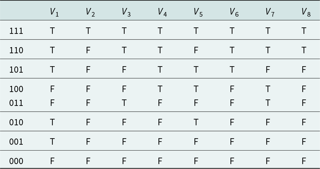
In this overall VGPA design, the proposed OSMSTP techniques is adopted in both drive and final stage as illustrated in Figure 3(b). Two amplification stages are introduced. The IOs and interstage of the VGPA are matched by transformers respectively and each active stage is in pseudo-differential operation. In the final stage, a 2:1 transformer is introduced for power combining. When all active devices are switching on, this VGA obtains its maximum gain. Only pulling down and pulling up status are used in this design so that no additional DAC is required to assist. The coding principle of this VGPA is to set two zones of gain switching by an on-chip 3–8 decoder. From VGPA’s full gain to its relative −21.0 dB, gain switching follows quasi equal division and its logic status is corresponding to 111-010. Basing on this division, state 010 is firstly picked up to be designed by the above gain degradation method. Following the rule of intermediate states in priority, 101 and 100 states are designed subsequently. Afterwards, 110 and 011 states are realized. From relative −21.0 to −60.0 dB, gain switching corresponds to logic status from 010 to 000. Its gain step is set to be gradually enlarged. Finally, control voltages for T1 to T8 are used to digitalize gain amplitude switching. They are coded by the 3–8 decoder in Figure 3(b) for control convenience. Its true table of controlling voltages in sub-cells is shown in Table 1. By this decoder, only one high level (2 V) and one low level (0 V) are enabled to control V 1–V 8.by increasing controlling bits or assign transistors in pseudo-differential operation with different partition.
(a) Circuit design criteria and its implementation procedures; (b) the proposed VGPA architecture (emitter length: t 1 – 0.9 μm, t 2 – 3.6 μm, t 3 – 1.8 μm, t 4 – 2.7 μm, t 5 – 0.9 μm, t 6 – 8.1 μm, t 7 – 1.8 μm, t 8 – 7.2 μm, t 9 – 4.5 μm, t 10 – 4.5 μm, t 11 – 9.0 μm, t 12 – 9.0 μm); (c) selectable gain levels.

The true table of controlling voltages in sub-cells

T – 2 V, F – 0 V.
If T1 to T8 in pseudo-differential operation is controlled by independent digits without this decoder, the original schematic could provide a maximum of 216 possible gain level selections. When T1 to T8 in pseudo-differential operation is controlled by V1 to V8 as designed, the 28 selectable gain levels are shown in Figure 3(c). At 94 GHz, the uncoded per-step could be as fine as 0.3 dB from its full gain to its relative −17.4 dB. From relative −17.4 to −39.9 dB, a per-step setting of 2.3 dB could be satisfied. In other custom designs, more possible coarse and fine gain switching sets could be selected
Measurement results
The proposed VGA was fabricated in 130 nm SiGe technology as shown in Figure 4. Its core area with on-chip digital decoder only occupies 310 × 102 μm2. Firstly, this DUT is characterized by PNA Network Analyzer. During this step, voltages V EX1–V EX3 to 3-bit control pads are switched between 0 and 2 V to represent 0 and 1 states. The tested V EX1–V EX3 levels also follow the designed values in Table 1. From 000 to 111 states, the S-parameter results agree well with simulation as shown in Figure 5(a). As expected, its gain switching steps of 111–010 are close to equal distribution. From 001 to 000 states, the VGPA is totally switched off. This gain step is about 18 dB. At 94 GHz, its gain dynamic range is 67.0 dB which is from 20.6 to −46.4 dB. At 000 states, this VGPA is totally switched off digitally by table without extra control motion and devices, which can also be used to turn off a channel in a phased-array. As the VGPA is switched off digitally by V EX1–V EX3 in Figure 3(b) while V cc and V bb are still on, the leakage current of the VGPA in state 000 is 4 mA during measurement. In system application, one or more channels could also be turned-off by a group of V EX1–V EX3 states without extra controlling to V cc and V bb For S 22 curves, the measurement and simulation results accord each other well. In the input and output matching schematics, both parts adopt transformers. The difference is that the input transformer is applied with metal insulator metal cap. Its modelling accuracy along with that of active devices could be a main reason accounts for deviations of S 11 center points to lower frequencies about 15% from 101 to 000 states. As input matching would directly affect gain level of an amplifier, this shift causes gain variations for 101–000 states. The measured and simulated phases of forward transmission S 21 are also plot in Figure 5(d). For 000 state, phase and amplitude deviates simulation due to discrepancies between simulating and modelling for transistor in the total cutting-off operation. In measurement, phase variation of S 21 is within a range of 43° at 94 GHz for the decoded states. In a phased array application with phase shifters, measurement data of all the states with information of amplitude and phase would be recorded and stored. According to scanning algorithm, certain data would be picked up for calibration of one channel and the final system. In this way, the mutual influence between phase and amplitude are considered in system view.
(a) The realized VGPA circuit in 130 nm SiGe; (b) the realized VGPA circuit in phased array.

The measured S-parameters. (a) S 21 in dB versus frequency; (b) S 11 in dB versus frequency; (c) S 22 in dB versus frequency; (d) S 21 phase in ° versus frequencies at different digital states.

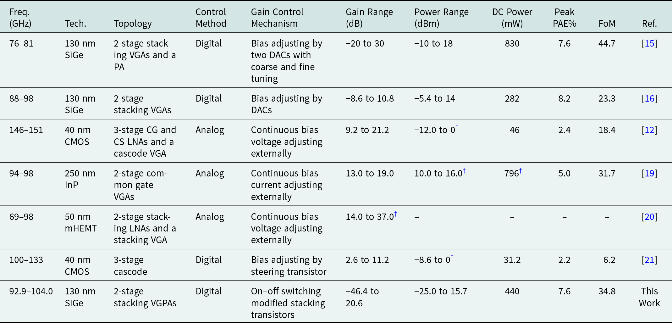
Then its output power is characterized with the aid of power meter and frequency sources. This DUT is measured under 2.5 V/4.0 V V cc and 1.2 V/1.5 V V bb as illustrated in Figure 6(a), which are recorded as low power (LP) and high power (HP) modes. In LP mode, the DUT at 111 state delivers output saturated power (P sat) of 8.5 dBm at 94 GHz and 8.0 dBm at 98 GHz. In HP mode, its P sat at 111 state would be boosted up to 15.7 dBm at 94 GHz and 15.3 dBm at 98 GHz. The P1dB of the output is 2.7 dBm and 9.5 dBm for LP and HP modes respectively at 94 GHz, as shown in Figure 6(d). As controlling bits switched from 111 to 000, its output power rolled down. When output power is below −25 dBm, it is hard to be detected by instruments. Therefore, the dynamic range of Pout at 94 GHz is estimated to be at least 40.7 dB in HP mode and 33.5 dB in LP mode. In Figure 6(b), its output power versus input is shown. In Table 2, the performances of this design are compared with state-of-the-art. This VGPA realizes large dynamic range both in gain and power at W band.
Large signal measurement. (a) Saturated output power at different digital states; (b) p out vs p in at HP mode at 94 GHz; (c) measured PAE vs p in at HP mode. (d) measured p sat and p 1db vs frequency.

VGA performances comparison with state-of-the-art

FoM = 10log(P out· G· PAE· f 2) [22]
† Estimated Value from the cited paper.
Conclusion
In this paper, digitization techniques of OSMSTP are proposed to free RF VGA’s abilities in large dynamic range, high response speed, fine and coarse gain control steps. Rather than bias continuous tuning or DAC dividing bias ranging, gain control digitization is directly achieved by on–off switching the lowest level transistors. Basing on the proposed techniques, a 3-bit digitalized W-band VGPA in 130 nm SiGe is fabricated and tested. It integrates two active stages with transformers and an on-chip 3-bit decoder. Its controllable gain and power dynamic ranges are above 60 and 41 dB, respectively, which are the highest reported so far. With on–off gain switching ways, this VGPA also provides 15.7 dBm peak output power with 1175.0 mW/mm2 power density. Moreover, the proposed OSMSTP provides a transplantable VGPA or VGLNA solution for other gain control tasks as long as upgrading units with more individual switching sets.
Acknowledgements
This work was supported in part by the Key Program of National Natural Science Foundation of China Grant 62131007.
Competing interests
None.

Jiang-An Han was born in Guilin, China, in 1984. He received the B.Sc. and M.Sc. degrees from the University of Electronic Science and Technology of China, Chengdu, China, in 2008 and 2011, respectively, and the Ph.D. degree from Nanyang Technological University, Singapore, in 2016. His research focuses on mmW/Terahertz circuit and system design in CMOS, and SiGe, GaAs and GaN technologies.

Xu Cheng was born in 1987. He received the B.E. degree in electromagnetics and wireless techniques from the University of Electronic Science and Technology of China, Chengdu. in 2009, and the Ph.D. degree in microelectronics and solid-state electronics from the Institute of Microelectronics, Chinese Academy of Sciences, Beijing, China, in 2014. From 2014 to 2017, he was an Assistant Professor with the Microsystem and Terahertz Research Center, China Academy of Engineering Physics, Chengdu. Since 2017, he has been an Associate Professor with the Microsystem and Terahertz Research Center, China Academy of Engineering Physics. His current research interests include microwave monolithic integrated circuits and analog baseband circuit designs.

Xian-Hu Luo received the B.E. degree from the University of Electronic Science and Technology of China. He joined Microsystem and Terahertz Research Center, China Academy of Engineering Physics, Chengdu, China, in 2017.

Liang Zhang received the B.E. degree from the Peking University. He has been an Associate Professor with the Microsystem and Terahertz Research Center, China Academy of Engineering Physics, Chengdu, China.

Zi-Qiang Yang was born in Chengdu, Sichuan, China, in 1981. He received the B.S. and Ph.D. degrees in electronic engineering from the University of Electronic Science and Technology of China (UESTC), Chengdu, China, in 2003 and 2008, respectively. In 2008, he joined the UESTC, as a Lecturer, and became an Associate Professor, in 2009. From 2013 to 2014, he was a Visiting Scholar with the Department of Electrical Engineering, Columbia University, New York, NY, USA. He has authored over 30 scientific journal papers and over ten conference papers. His research interests include microwave monolithic integrated circuits, microwave passive components, antennas, and metamaterials.

Bin-Bin Cheng was born in Hubei, China, in 1980. He received the B.S. and Ph.D. degrees in engineering physics from Tsinghua University, Beijing, China, in 2004 and 2009, respectively. From 2006 to 2007, he was a Research Assistant with the European Organization for Nuclear Research (CERN), Geneva, Switzerland. He joined the Institute of Electronic Engineering (IEE), China Academy of Engineering Physics (CAEP), Mianyang, China, in 2009. He is currently a Researcher with the Microsystem and Terahertz Research Center, CAEP, Chengdu, China. His current research interests include millimeter-wave (mmW)/terahertz radar and imaging systems.

Chang-Xing Lin received the B.S. degree in engineering physics and the Ph.D. degree in nuclear science and technology from Tsinghua University, Beijing, China, in 2007 and 2012, respectively. From June to December 2009, he was a Research Assistant with the European Organization for Nuclear Research, Switzerland. In 2012, he joined the Institute of Electronic Engineering, China Academy of Engineering Physics, Mianyang, China. His current research interests involve algorithm and implementation of high-speed demodulation and terahertz wireless local area networks.

Xian-Jin Deng was born in Sichuan, China, on June 11, 1973. He received the B.S. degree in electronic engineering from Xidian University, Xian, China, in 1998. He received the M.S. degree in electronic science and techniques from University of Electronic Science and Technology of China, Chengdu, China, in 2006. He joined the Institute of Electronic Engineering (IEE), China Academy of Engineering Physics (CAEP), Mianyang, China, in 2003. His current research involves mmW/Terahertz communication system, mmW solid-state power combining, and microwave active circuits.