I. INTRODUCTION
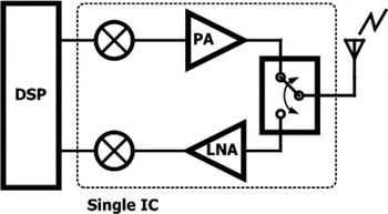
The recent steep growth of mobile phones with embedded Wi-Fi has given rise to demand for a low-cost system solution [Reference Francois and Reynaert1–Reference Yin, Yu, Wang and Chi4]. Fully integrated transceivers including RF power amplifiers for wireless local area network (WLAN) solutions, as illustrated in Fig. 1, are considered an essential technology to develop a low-cost system [Reference Ryu, Jang, Lee and Jeong5, Reference Ryu, Park and Jeong6]. However, in general, power amplifiers for WLAN applications have been designed using compound semiconductors because of the requirements of high peak to average power ratio (PAPR) and peak output power in the WLAN standard. Although compound semiconductor based power amplifiers appear to have higher linearity and output power than those of CMOS-based power amplifiers, the latter are essential to achieve fully integrated transceivers for WLAN applications. In tandem with recent advances in CMOS technology, several studies on the development of CMOS power amplifiers have been introduced [Reference Koo, Joo, Na and Hong7–Reference Kaymaksut, Zhao and Reynaert10]. However, most CMOS power amplifiers for WLAN applications are focused on an operating frequency of 2.4 GHz. There have been few works related to CMOS power amplifiers for the IEEE 802.11n standard with operating frequencies of 5.0 GHz.
Simplified block diagram of single IC for WLNA applications.

In this study, we designed a 5.0 GHz CMOS power amplifier using 180-nm SOI RFCMOS technology for IEEE 802.11n WLAN applications. Although we designed a stand-alone CMOS power amplifier in this work, we proposed a split inductor for the inter-stage matching network to minimize the chip area of the power amplifier and increase the possibility of developing a fully integrated transceiver for WLAN applications. At the same time, we designed the split inductor in the inter-stage matching network to minimize mismatches in the differential signal and thereby improve the overall system output power.
II. TYPICAL LAYOUT OF THE CMOS POWER AMPLIFIER
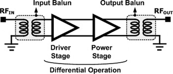
In general, a RF CMOS power amplifier is designed using a differential structure to minimize the gain reduction problems induced by undesired parasitic components of the bond wires, as shown in Fig. 2. Given that the differential structure provides a virtual ground in the RFIC, this structure is widely used in CMOS integrated circuits (ICs), in which a through-via-hole is not provided. Accordingly, input and output baluns are required to support the differential operation of the general RF CMOS power amplifier.
Simplified block diagram of RF CMOS power amplifiers.

Additionally, as shown in Fig. 2, a RF CMOS power amplifier is constructed with a multi-stage structure to obtain sufficient gain. The power stage of the power amplifier generates the required high power in the given wireless standard. On the other hand, the driver stage of the power amplifier provides sufficient gain and generates the drive signal for the input of the power stage. In general, at least one inductor is required in each stage of the linear RF power amplifier to amplify the RF signal with high linearity. Unfortunately, integrated inductors require bulky chip area, and the bulky size of the inductor makes it difficult to design the layout properly with minimized chip size and good signal quality. In particular, the inductor for the driver stage of the differential power amplifier should be properly located in the IC to minimize both the additionally required chip area and the degradation of the RF signal quality.
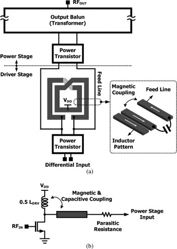
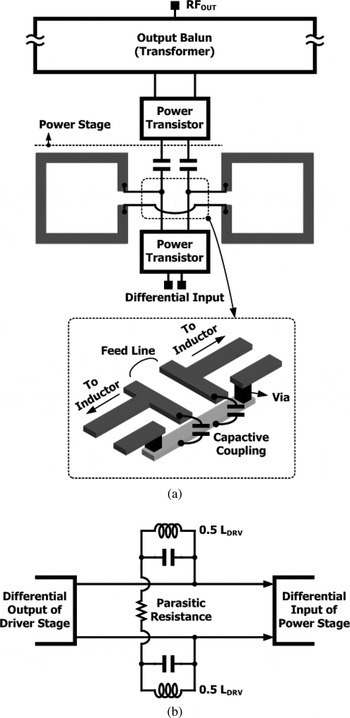
One way to design the layout of the driver stage inductor is shown in Fig. 3. In this method, a single differential inductor is used for the driver stage inductor and the differential signal lines for the interconnection between the output of the driver stage and the input of the power stage circle the inductor, as shown in Fig. 3(a). In this case, given that the inductor is positioned with a symmetric layout, the mismatch in the differential signal lines is minimized. However, because the feed lines should circle the inductor to minimize the undesired magnetic coupling between the feed lines and the inductor, the loss induced by the parasitic resistance of the feed lines degrades the performance of the amplifier. Additionally, as can be predicted from the layout shown in Fig. 3(a), the overall chip size of the power amplifier increases. Fig. 3(b) shows a simplified equivalent circuit of the typical symmetric layout.
Typical symmetric layout of the driver stage inductor: (a) conceptual layout and (b) equivalent half-circuit.

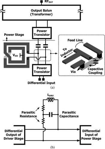
Another way of designing the layout of the driver stage inductor is shown in Fig. 4(a). In this method, a single differential inductor is used for the driver stage inductor and the differential signal lines for the interconnection between the output of the driver stage and the input of the power stage are shortened compared with those used in the typical symmetric layout shown in Fig. 3(a). In this case, given that the differential interconnection lines are shortened, the loss induced by the parasitic resistance of the interconnection lines is minimized. Additionally, the overall chip size for the asymmetric layout is reduced compared with that for the typical symmetric layout. However, given that the inductor is positioned with an asymmetric layout, a mismatch in the differential signal lines arises and therefore the performance of the power amplifier drops. As can be seen in Fig. 4(a), the usage of via-holes is essential where the two metal lines cross over. Fig. 4(b) presents a simplified equivalent circuit of the typical asymmetric layout. The parasitic resistances induced by the via-hole are directly connected to one of the differential lines. Accordingly, the ideal differential characteristic is broken, as shown in Fig. 4(b).
Typical asymmetric layout of the driver stage inductor: (a) conceptual layout and (b) equivalent circuit.

Moreover, the asymmetry between the differential signals can be intensified according to the process variation. For example, if there is no process variation, the asymmetry can be compensated using additional matching components. However, if the process variation is considered, it is difficult to remove the asymmetry completely.
III. PROPOSED SPLIT INTER-STAGE INDUCTOR
In this study, to minimize the mismatches between the differential signal lines and the losses induced by the parasitic resistances of the interconnection lines, we propose a symmetric layout for the inter-stage inductor.
The proposed layout of the split inter-stage inductor is shown in Fig. 5(a). In the proposed layout, an inductor for the typical layout is split into two identical inductors. Although via-holes are used in the region where the metal lines cross over, the impedance values, including those of all the parasitic components looking into the shunt inductor from the differential signal lines, are identical to each other, as shown in Fig. 5(b). Accordingly, the proposed layout technique of the split inter-stage inductor can minimize mismatches between the differential lines. Given that, even allowing for process variation, the impedances for the differential signals are nearly identical to each other, and the symmetry characteristic is maintained. Additionally, considering that the length of the interconnection lines between the output of the driver stage and the input of the power stage is nearly identical to that of the typical asymmetric layout shown in Fig. 4(a), the parasitic resistance and the overall chip size can be minimized and are nearly identical to those of the typical asymmetric layout.
Proposed symmetric layout using a split inter-stage inductor: (a) conceptual layout and (b) equivalent circuit.

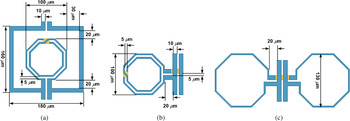
Figure 6 shows the layouts used in the 2.5-dimensional electromagnetic (2.5D EM) simulation conducted to verify the feasibility of the proposed layout technique. The metal width of the inductor is 3 µm.
As can be seen in Fig. 6, the required area of the proposed layout associated with the inductor is largest among those of the three layouts. However, if we consider the actual layout of the inductors in the power amplifier, as shown in Figs 3–5, the overall chip size of the power amplifier using the proposed symmetric layout technique is nearly identical to that of the power amplifier using the typical asymmetric layout. For example, if the typical symmetric layout shown in Fig. 6(a) is used in the power amplifier, the height of the inductor should be at least greater than 160 µm, as can be predicted from Fig. 6(a), while the right and left sides of the inductor are left unused, as shown in Fig. 3. On the other hand, if the typical asymmetric layout shown in Fig. 6(b) is adopted in the power amplifier, the overall chip size can be minimized. For the typical asymmetric layout, the required height is approximately 100 µm, as shown in Fig. 6(b), while the right side of the inductor is left unused. For the proposed symmetric layout, the required height is approximately 130 µm with full use of both sides of the inductor.
Layouts for 2.5D EM simulations: (a) typical symmetric layout, (b) typical asymmetric layout, and (c) proposed symmetric layout.

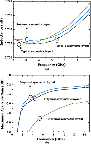
Figure 7 shows simulated results of the three layout techniques. As shown in Fig. 7(a), the simulated inductances of the three layout techniques are almost identical at 0.7 nH. In Fig. 7(b), the simulated maximum available gains (MAGs) of the three layout techniques are provided. As can be seen in this figure, the loss induced by the typical symmetric layout for the inter-stage inductor is the highest among the three layout cases. In the typical symmetric layout, given that mismatches between the differential signal lines are minimized, the resistive loss induced by the long interconnection lines is dominant. On the other hand, the dominant cause of the loss in the typical asymmetric layout is the mismatches in the differential signal lines. As can be seen in Fig. 7(b), the overall loss of the proposed symmetric layout technique is the lowest among the three layout techniques.
Simulation results: (a) inductance and (b) MAG.

IV. DESIGN OF A CMOS POWER AMPLIFIER USING THE PROPOSED SPLIT INTER-STAGE INDUCTOR
To verify the feasibility of the proposed split inter-stage inductor, a CMOS power amplifier that has an operating frequency of 5.0 GHz for 802.11n WLAN applications is designed using a 180-nm SOI RFCMOS process. The CMOS process provides four metal layers with 4 µm thickness of the top metal layer.
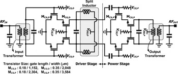
A simple schematic of the designed power amplifier is shown in Fig. 8. Transformers are used in the input and output parts as the input and output baluns. The transformers are designed using a 2.5D EM simulator. The EM simulation is performed for the frequency range of DC to 20 GHz to predict the DC loss and also up to 2nd and 3rd harmonic components. The top metal layer is used in the input and output transformers to minimize undesired cross-talk between transformers and other interconnection lines. The 3rd metal layer is partially used in the cross over region of the metal lines in the transformers. The outer size of the input and output transformers is 0.25 × 0.25 mm2 and 0.5 × 0.4 mm2, respectively.
Schematic of the CMOS power amplifier using the proposed split inter-stage inductor.

The driver and the power stages are designed with differential structures. A cascode structure is used in these stages to improve the reliability. To obtain sufficient gain, the common-source transistors of the driver and power stages are composed of a NMOS with 180-nm gate length. To mitigate the voltage stress, the common-gate transistors of the drive and power stages are composed of a NMOS with 350-nm gate length. To mitigate the output power and efficiency degradation induced by the common-gate transistors, we designed the width of the common-gate transistor to be larger than that of the common-source transistor.
The proposed split inductor is used in the inter-stage matching network. The supply voltage of the driver stage enters through the center between the split inductors, as shown in Fig. 8. Similarly, the supply voltage of the power stages enters through the center tap of the primary part of the output transformer, as shown in Fig. 8. In this work, the supply voltage for the driver and power stages is 3.3 V, respectively.
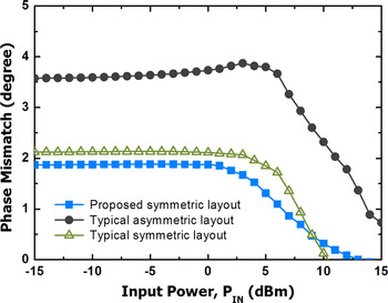
To verify the feasibility of the proposed technique, we simulate the power amplifiers using the three layout techniques. Figure 9 shows the simulated phase mismatches between differential signals in the drain node of M CG,D for the three layout techniques. The phase mismatches are simulated according to the input power. As can be seen in Fig. 9, the phase mismatches for the typical and the proposed asymmetric layouts are nearly identical to each other. On the other hand, the phase mismatch for the typical asymmetric layout is approximately 1.5 times higher than that of the symmetric layout.
Simulation results at 5.0 GHz: phase mismatch for the three layout techniques.

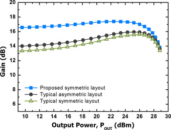
Figure 10 shows the simulated power gain of the designed power amplifier using the three layout techniques. As shown in Fig. 10, the gain of the power amplifier using the proposed symmetric layout technique is highest among the three layout techniques. The loss of the power amplifier using the typical asymmetric layout is mainly induced by the mismatches between differential signals, as can be predicted from the simulation results shown in Fig. 9. On the other hand, the loss of the power amplifier using the typical symmetric layout is mainly induced by the loss of the feeding lines that circle the inductor, as shown in Fig. 6(a).
Simulation results at 5.0 GHz: gain according to output power with CW input signal.

V. MEASUREMENT RESULTS
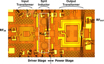
Figure 11 provides a photograph of the designed CMOS power amplifier, which has a chip size of 1.42 × 0.75 mm2. All of the matching components, including the test pads, are fully integrated. We measured the performance of the designed CMOS power amplifier using a continuous wave (CW) signal and a WLAN-modulated signal (64 QAM, 20 MHz bandwidth). The bare chip is mounted on a printed circuit board for measurement. Because of the fully-integrated power amplifier, there are no additional off-chip matching components on the PCB. All of the measured results are obtained with 50-Ω input and output load impedances. A signal generator, spectrum analyzer, and 20-dB attenuator for the output port are used. The losses of the bond wires are not de-embedded. The effects of the bond wires are considered in the simulation.
Photograph of the designed power amplifier.

Although the target frequency of the designed power amplifier is 5.0 GHz, because of the undesired parasitic components, the optimum operating frequency of the power amplifier is down-shifted. Figure 12 shows the measured gain and power added efficiency (PAE) according to the output power, P OUT, with 4.47-GHz CW input power. The measured maximum output power is 27.3 dBm with a PAE of 28.0%. In general, power amplifiers show the gain compression phenomenon near the saturation power region. However, given that the designed power amplifier is destroyed owing to the breakdown phenomenon of the transistor in the saturation output power region using the CW input signal, the gain, output power, and PAE of the linear region are shown in Fig. 12.
Measured versus simulated results at 4.47 GHz: gain and PAE with CW input power.

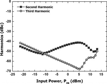
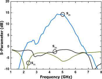
Figure 13 shows the measured second and third harmonics versus the CW input power. As can be seen in Fig. 13, the powers of the harmonics are approximately −40 dBc lower than the fundamental output power for the input power swept range. The low second harmonics power indicates that the mismatch in the differential signals of the designed power amplifier is minimized. Figure 14 shows the measured S-parameters with the CW input signal. The measured small signal gain is approximately 14 dB for the frequency range of 4.5–5.0 GHz.
Measured results at 4.47 GHz: second and third harmonics according to CW input power.

Measured results: S-parameters.

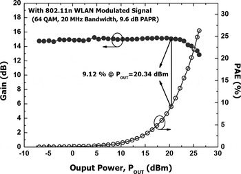
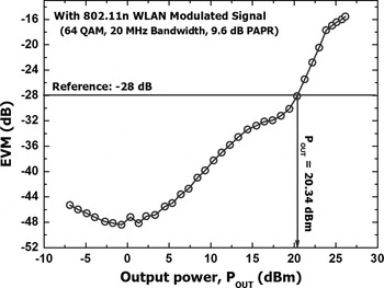
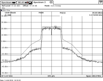
The power amplifier is also measured using WLAN 802.11n (OFDM 64-QAM 65 in 20 MHz bandwidth). Figure 15 shows the measured gain and PAE with a 4.47 GHz 802.11n signal. The power amplifier achieved 9.12% PAE at an output power of 20.34 dBm. In Fig. 16, the measured EVM for the 802.11n input signal is shown. As can be seen in this figure, the maximum output power at which the 802.11n standard is met is 20.34 dBm. In Fig. 17, the output spectrum of the power amplifier for the 4.47 GHz 802.11n signal is shown. As can be seen in Fig. 17, the spectral mask is successfully met.
Measured results at 4.47 GHz: gain and PAE with WLAN-modulated input signal.

Measured results at 4.47 GHz: EVM for the 802.11n input signal.

Output spectrum of the power amplifier for 4.47 GHz 802.11n signal at P OUT of 20 dBm.

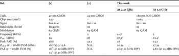
Table 1 provides the results of recently reported CMOS power amplifiers for 5-GHz WLAN applications for comparison. Most recent works related to power amplifiers for 5.0-GHz WLAN applications are designed using 40- and 65-nm CMOS technology or 180-nm BiCMOS technology to meet the linearity requirement of the WLAN standard. In particular, the 802.11ac/n/g standard requires high PAPR performance. In this work, we demonstrate the possibility of a CMOS power amplifier using 180-nm CMOS technology for 5.0 GHz 802.11n WLAN applications.
Comparison with state-of-the-art power amplifiers for 5-GHz WLAN applications.

* Measured maximum output power.
† Graphically inferred.
VI. DISCUSSION
In Fig. 10, the gain of the power amplifier using the typical asymmetric layout is approximately 2 dB lower than that using the proposed symmetric layout. Although the resistive loss induced by the feeding lines that circle the inductor, as shown in Fig. 6(a), affects the gain, the parasitic capacitance of the feeding lines also degrades the gain of the power amplifier. However, the parasitic capacitance of the feeding lines can be canceled out using additional matching components. Accordingly, if the parasitic capacitance of the feeding lines of the typical asymmetric layout is properly embedded in the inter-stage matching network, the gain of the power amplifier using the typical asymmetric layout shown in Fig. 10 can be improved.
The target frequency of the designed power amplifier is 5.0 GHz. However, because of the unpredicted parasitic components, for example, dummy patterns for the density rule in the output transformer, the optimum operating frequency of the power amplifier is down-shifted and S 11 and S 22 are degraded, as shown in Fig. 14. At the operating frequency of 5.0 GHz, the maximum linear output power that meets the IEEE 802.11n MCS 7 standard is measured as 17.34 dBm with 4.82% PAE.
V. CONCLUSION
In this study, we designed a CMOS power amplifier for WLAN 802.11n (64-QAM, 20 MHz bandwidth, 9.6 dB PAPR) applications. To minimize the overall chip area and the mismatch in the differential signals, a split inter-stage inductor is proposed. Using the proposed split inductor, we can reduce the overall chip area, while mismatch in the differential signals is minimized compared with that of the typical layout techniques. To verify the feasibility of the proposed power amplifier, we designed the power amplifier using a 180-nm SOI RFCMOS process. The designed power amplifier is fully integrated, including the input and output matching network, input and output transformers, and test pads. The chip size of the designed power amplifier is 1.065 mm2. The measured maximum linear output power is 20.34 dBm, while the measured EVM for the 802.11n input signal is −28 dB. From the measured results, we confirm the feasibility of the proposed CMOS power amplifier.
ACKNOWLEDGEMENTS
This work was supported by the International Collaborative R&D Program (N0000899), funded by the Ministry of Trade, Industry and Energy (MKE, Korea).
 Minoh Son received his B.S. and M.S. degrees in Electronic Engineering from Soongsil University, Seoul, in 2014 and 2016, respectively. His current research interests include CMOS RF power amplifiers.
 Jinho Yoo received his B.S. and M.S. degrees in Electronic Engineering from Soongsil University, Seoul, in 2013 and 2015, respectively, and is currently working toward a Ph.D. at Soongsil University. His current research interests include CMOS RF power amplifiers.
 Inseong Kang received his B.S. and M.S. degrees in Electronic Engineering from Soongsil University, Seoul, in 2013 and 2015, respectively, and is currently working toward a Ph.D. at Soongsil University. His current research interests include millimeter-wave power amplifiers.
 Changhyun Lee received his B.S. and M.S. degrees in Electronic Engineering from Soongsil University, Seoul, in 2011 and 2013, respectively, and is currently working toward a Ph.D. at Soongsil University. His current research interests include CMOS RF power amplifiers and transceivers for wireless chip-to-chip communication.
 Jihoon Kim received his B.S., M.S degrees in Radio Communication Engineering from Kyung-Hee University, Suwon, Korea, in 2009 and 2013, respectively. From 2014 to now, he is working in Gigalane Inc., Hwaseong, Korea. His research interests include RF & Millimeter-wave circuits.
 Ho Jong Park received his M.S. degrees in Electrical and Computer Engineering from Pusan National University, Busan, Korea, in 2015. He is currently a researcher with GigaLane, Hwaseong, Korea. His research interests include RFICs and PMICs.
 Young-Bae Park received his B.S., M.S., and Ph.D. degrees in Radio Engineering from the Korea Maritime University, Busan, Korea, in 2005, 2007, and 2011, respectively. He is currently a researcher with the Gigalane, Hwaseong, Korea. His research interests include RFICs, microwave, and millimeter-wave-integrated circuits.
 Changkun Park received his B.S., M.S., and Ph.D. degrees in Electrical Engineering from Korea Advanced Institute of Science and Technology (KAIST), Daejeon, Korea, in 2001, 2003, and 2007, respectively. From 2007 to 2009, he was with the Advanced Design Team of the DRAM Development Division, Hynix Semiconductor Inc., Icheon, Korea, where he was involved in development of high-speed I/O interfaces of DRAM. In September of 2009, he joined the faculty of the School of Electronic Engineering, Soongsil University, Seoul, Korea. His research interests include RF and millimeter-wave circuits, RF CMOS power amplifiers, and wireless chip-to-chip communication and power transfers.