
Introduction
Nickel (Ni) and nickel carbide (Ni3C x ) thin films have many important applications. For instance, Ni films have been used in ultra-large-scale integrated-circuit devices for preparing low-resistivity Ni-silicide contacts.[ Reference Kittl, Lauwers, Chamirian, Van Dal, Akheyar, De Potter, Lindsay and Maex 1 , Reference Ha, Yun and Lee 2 ] Ni films have also been used in many microelectromechanical systems (MEMS), such as micro-cantilevers and micromechanical switches.[ Reference Zavracky, Majumder and McGruer 3 – Reference Teh, Luo, Graham, Pavlov and Smith 5 ] Also, since Ni is an important element in catalysis, synthesizing Ni and its compounds as thin films are also of great importance for catalysis applications.[ Reference Li, Shao, Su, Gao and Wang 6 , Reference Xiong, Guo, Guo, Li, Zhao, Chen, Liu and Wang 7 ]
Common fabrication methods for Ni and Ni3C x thin films include physical vapor deposition (PVD), chemical vapor deposition (CVD), and atomic layer deposition (ALD). PVD is capable of fabricating high-purity films, but the step coverage of the PVD films is rather poor, which could largely limit its applications to conformal film coatings on non-flat trench or hole structures. CVD and ALD are generally better for film step coverage.[ Reference Yanguas-Gil, Yang, Kumar and Abelson 8 , Reference George 9 ] In particular, ALD is known for depositing films with high uniformity and conformality on high-aspect-ratio complex structures[ Reference George 9 – Reference Gao, Shao, Yan, Li, Su, Meng and Wang 15 ]; however, the deposition rate of ALD is comparatively slow. CVD is generally faster than ALD in the deposition rate, but the film quality relies very much on the control of the CVD parameters (e.g., gas flow control).[ Reference Yanguas-Gil, Yang, Kumar and Abelson 8 ] Normally, CVD processes are run in a continuous deposition mode, where the metal precursor vapor and the coreactant gas (if needed) are continuously and simultaneously delivered into the deposition chamber. But the metal precursor vapor can also be instead pulsed into the deposition chamber, and this type of CVD is also known as pulsed chemical vapor deposition (PCVD).[ Reference Wang and Gordon 16 , Reference Wang and Gordon 17 ] The metal precursor itself is very important for both CVD and ALD, and the development of new metal precursors is a core task in the CVD and ALD research areas. Over the years, there have been a number of Ni precursors reported for the CVD and ALD of Ni and Ni3C x thin films. For instance, bis(cyclopentadienyl)nickel or its derivative, bis(ethylcyclopentadienyl)nickel, was used with H2 or NH3 for the CVD and ALD of Ni metal[ Reference Protopopova and Alexandrov 18 – Reference Wang, Ding, Liu, Liu, Ding and Zhang 20 ]; Ni acetylacetonate was used with H2 or a primary alcohol for the ALD and CVD of Ni or Ni3C x [ Reference Sarr, Bahlawane, Arl, Dossot, McRae and Lenoble 21 – Reference Premkumar, Bahlawane and Kohse-Höinghaus 23 ]; bis(dimethylamino-2-methyl-2-butoxo)nickel was used with H2 or NH3 plasma for the ALD of Ni metal[ Reference Han-Bo-Ram, Sung-Hwan, Woo-Hee, Gil Ho, Young Kuk, Taek-Mo, Chang Gyoun, Chan Gyung and Hyungjun 24 ]; bis(N,N ′-dialkylacetamidinato)nickel(II) was used with H2 for the ALD and CVD of Ni metal[ Reference Li, Gordon, Pallem, Li and Shenai 25 , Reference Lim, Rahtu and Gordon 26 ]; bis(1,4-di-isopropyl-1,3-diazabutadienyl)nickel was used with NH3 plasma for the ALD of Ni metal[ Reference Kim, Jang, Park, Jeon, Kim, Yuh and Jeon 27 ]; and very recently a similar compound of bis(1,4-di-tert-butyl-1,3-diazabutadienyl)nickel(II) was used with H2 plasma for the ALD of Ni3C.[ Reference Xiong, Guo, Guo, Li, Zhao, Chen, Liu and Wang 7 ]
In this work, we report a new PCVD process to deposit Ni and Ni3C x thin films, using bis(1,4-di-tert-butyl-1,3-diazabutadienyl)nickel(II) [Ni(dad)2] as the Ni precursor. The Ni(dad)2 compound is highly volatile, and it does not contain oxygen in its molecular structure, so it can avoid the incorporation of oxygen impurities in films. We used either molecular H2 gas or H2 plasma as the coreactant, and their effects on the properties of the PCVD films were carefully investigated.
Experimental
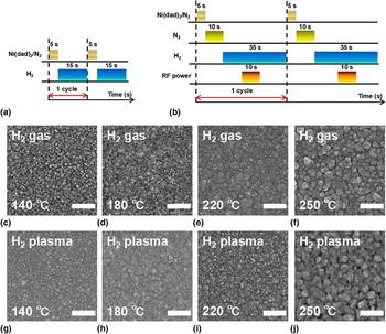
The PCVD system had a tubular deposition chamber, which was made of a 60 cm long fused-silica tube. The upstream part of the tube was wrapped with a copper coil, through which pulsed radiofrequency (RF) power could be supplied to generate plasma inside the upstream zone of the tube. A detailed description of the deposition system can be found in our previous publication.[ Reference Guo, Li, Chen, Sang, Yang, Liu and Wang 28 ] The Ni precursor Ni(dad)2 was kept in a glass container, and its vapor was delivered into the deposition chamber with the use of pure nitrogen (N2) gas as the carrier gas. During deposition, the Ni(dad)2 precursor was heated to 90 °C to afford sufficient vapor pressure, and the flow rate of the N2 carrier gas was kept at 50 sccm. Pure hydrogen (H2) gas or H2 plasma was used as the coreactant in PCVD. The H2 gas flow rate was kept at 50 sccm, and the aforementioned pulsed RF power (13.56 MHz, 60 W) was used to generate the H2 plasma. The PCVD process was run in a cyclic manner. For the deposition using H2 gas, each cycle consisted of a 5 s Ni(dad)2 pulse and a 15 s H2 gas pulse; whereas for the deposition using H2 plasma, each cycle consisted of a 5 s Ni(dad)2 pulse, a 10 s N2 gas pulse, a 10 s H2 gas pulse, a 10 s H2 plasma pulse, and a 15 s H2 gas pulse in sequence. Figures 1(a) and 1(b) schematically illustrate the process details. The N2 and H2 gas pulses between the Ni(dad)2 and H2 plasma pulses were used to stabilize the gas flow when switching the gas type. The total number of the Ni(dad)2 pulses was 500 or 250 for the films deposited using H2 gas or H2 plasma, respectively. We used a smaller number of pulses for the latter case because the films grew much faster when using H2 plasma as the coreactant. The deposition temperature was varied from 140 to 250 °C to study the temperature effect, and all these temperatures were beyond the onset thermal decomposition temperature of the Ni(dad)2 precursor.[ Reference Xiong, Guo, Guo, Li, Zhao, Chen, Liu and Wang 7 ] Si wafers and glass slides were used as the substrates, and no appreciable difference was observed for the films deposited on these two types of substrates. Prior to PCVD, all the substrates were sequentially cleaned with acetone, methanol, and isopropanol, and then pretreated by 1 min of H2 plasma.
(a) and (b) Schematic illustration of the PCVD processes using (a) H2 gas or (b) H2 plasma as the coreactant. (c)–(j) Representative SEM images of the PCVD films deposited at various different temperatures using (c)–(f) H2 gas or (g)–(j) H2 plasma as the coreactant. All scale bars represent 200 nm.

The PCVD films were carefully characterized by various techniques. The film thickness was measured by first scratching the deposited film and then measuring the step profile (Veeco, Plainview, NY, USA, Dektak 150) across the scratched line, and the obtained thickness was also verified by cross-sectional scanning electron microscopy (SEM) (Hitachi, Tokyo, Japan, SU8020). SEM was also used to examine the surface morphology of the films. The film composition was analyzed by x-ray photoelectron spectroscopy (XPS) (Thermo Scientific, East Grinstead, UK, Escalab 250Xi), and the film crystallinity was analyzed by x-ray diffraction (XRD) (Rigaku, Tokyo, Japan, D/max-2200 PC). The microstructure of the films was examined by transmission electron microscopy (TEM) (Jeol, Tokyo, Japan, JEM-3200F). Raman spectra were collected by a Raman spectrometer (Titan, Beijing, China, RTS-2) using an excitation wavelength of 532 nm. The film sheet resistance was measured by four-point probes method (Probes Tech, Guangzhou, China, RTS-8).
Results and discussion
Table I lists the thicknesses of the PCVD films deposited using H2 gas or H2 plasma as the coreactant at various deposition temperatures from 140 to 250 °C. For either type of the coreactants, the film thickness showed an increasing trend with the deposition temperature from 140 to 200 °C, and beyond 200 °C the thickness remained roughly the same. Note that the total number of the Ni(dad)2 pulses was 500 or 250 for the films deposited using H2 gas or H2 plasma, respectively, but the film thicknesses in the two cases were roughly the same for each deposition temperature, which therefore indicates that the deposition rate was about two times larger when using H2 plasma as the coreactant, as compared with the case using H2 gas.
Thicknesses of the films deposited by PCVD in this work. The thickness values are presented in the unit of nm. The total number of the Ni(dad)2 pulses was 500 or 250 for the films deposited using H2 gas or H2 plasma, respectively.

The surface morphologies of the PCVD films were examined by SEM. Figures 1(c)–1(j) show the representative SEM images of the films deposited with H2 gas or H2 plasma at various temperatures ranging from 140 to 250 °C. The films were all found to be continuous, and they could cover the entire substrates with no apparent pinholes through the films. The deposition temperature was found to have an effect on the film grain size, as the grain size increased when the temperature increased. This temperature effect was particularly pronounced for the highest temperature case (250 °C), possibly owing to a much-enhanced surface atom diffusivity at high temperature, which thereby led to a considerable increase in the film grain size.
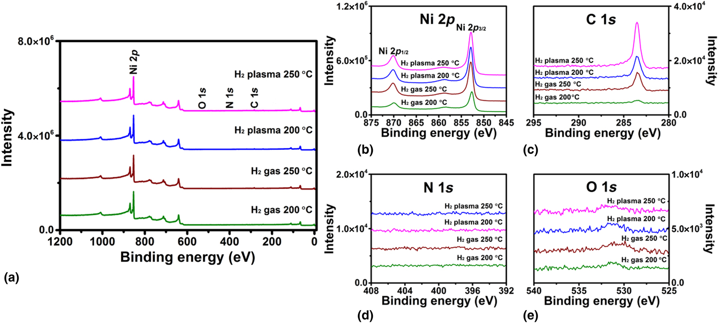
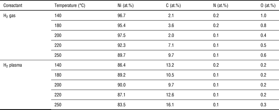
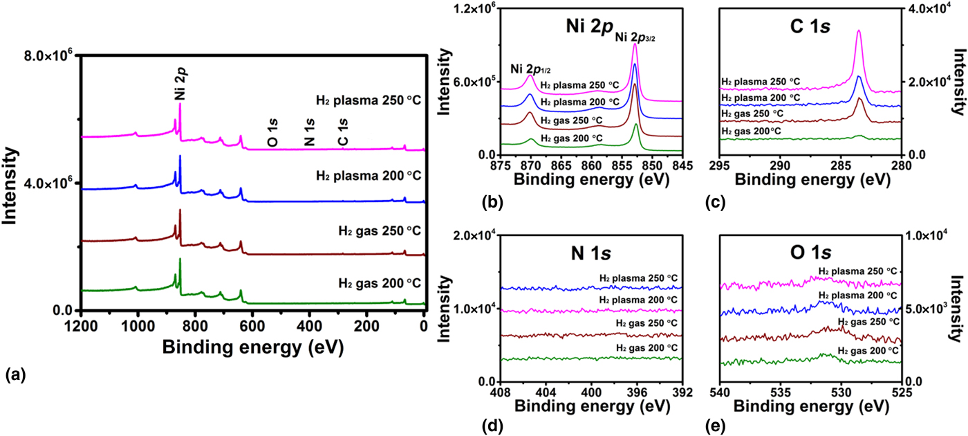
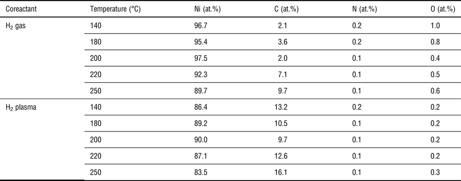
The elemental compositions of the PCVD films were analyzed by XPS. Prior to the XPS data collection, all the samples were subject to 100 s of 2 kV Ar+ sputtering to remove the surface oxide and adventitious carbon. Figure 2 shows representative XPS results for the films deposited at 200 and 250 °C using H2 gas or H2 plasma as the coreactant. (The spectra for other deposition conditions are not shown here, as they contain similar information, but their analysis results are included in the following Table II.) Figure 2(a) shows the survey spectra and Figs. 2(b)–2(e) show the high-resolution spectra of Ni 2p, C 1s, N 1s, and O 1s core-level emissions. The peaks appeared in the survey spectra [Fig. 2(a)] were found to be all from the Ni and C photoelectron emissions; and the high-resolution spectra [Figs. 2(d)–2(e)] further show that the amounts of the possible impurities of N and O were both fairly small. Using the areas of the peaks as shown in Figs. 2(b)–2(e), the elemental compositions of the PCVD films were extracted and are listed in Table II. Table II includes the film composition results for all the deposition conditions used in this work. We found that all the PCVD films were quite pure, as the N and O impurity levels were all below 0.2 and 1.0 at.%, respectively. Also, the C content was found to be fairly low for the films deposited with H2 gas at low temperatures ≤200 °C (2.0–3.6 at.%), and thus, under these conditions, the deposited films were actually Ni metal (with minor C impurity). However, for the films deposited at a higher temperature (≥220 °C) and/or with H2 plasma, the C content was considerably higher and it could be as high as 16.1 at.% for the films deposited at 250 °C with H2 plasma. As will be shown later, under these conditions, the deposited films were actually Ni3C x . In addition, the binding energies of the Ni 2p 3/2 peaks were found to be different for the above two cases. As the representative curves are shown in Fig. 2(b), the Ni 2p 3/2 binding energy for the films deposited at 200 °C with H2 gas was found at 852.7 eV, which is in line with Ni metal[ Reference Xiong, Guo, Guo, Li, Zhao, Chen, Liu and Wang 7 , Reference Goto, Taniguchi, Omata, Otsuka-Yao-Matsuo, Ohashi, Ueda, Yoshikawa, Yamashita, Oohashi and Kobayashi 29 ]; whereas for the remaining three conditions, all the Ni 2p 3/2 binding energies shifted to a greater number of 852.9 eV, which is an indicator for the formation of Ni–C bonds as previously reported.[ Reference Xiong, Guo, Guo, Li, Zhao, Chen, Liu and Wang 7 , Reference Goto, Taniguchi, Omata, Otsuka-Yao-Matsuo, Ohashi, Ueda, Yoshikawa, Yamashita, Oohashi and Kobayashi 29 ] Also, the binding energies of C 1s were all found at 283.5 eV, which is a typical number for Ni3C x .[ Reference Xiong, Guo, Guo, Li, Zhao, Chen, Liu and Wang 7 , Reference Goto, Taniguchi, Omata, Otsuka-Yao-Matsuo, Ohashi, Ueda, Yoshikawa, Yamashita, Oohashi and Kobayashi 29 ] But it should be noted that, in all the cases, the C contents were lower than that of the stoichiometric Ni3C (i.e., 25 at.%).
Representative XPS results for the PCVD films deposited at 200 and 250 °C using H2 gas or H2 plasma as the coreactant. (a) Survey spectra and high-resolution spectra for (b) Ni 2p, (c) C 1s, (d) N 1s, and (e) O 1s core-level emissions.
Summary of the elemental compositions of the PCVD films. Data were extracted from XPS results.
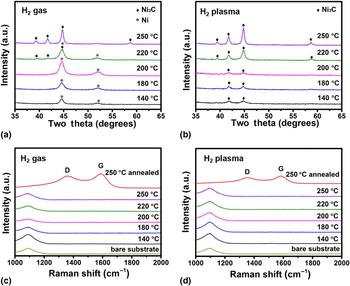
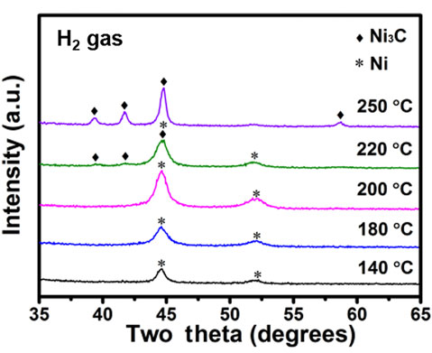
The crystallinities of the PCVD films were examined by XRD. Figures 3(a) and 3(b) show the XRD spectra of the films deposited with H2 gas [Fig. 3(a)] or H2 plasma [Fig. 3(b)] at various temperatures from 140 to 250 °C. All the films exhibited crystalline diffraction peaks, and the diffraction peaks were identified to belong to a faced-centered cubic (fcc) Ni phase (PDF#04-0850) and/or a rhombohedral Ni3C phase (PDF#06-0697). As shown in Fig. 3(a), for the films deposited at ≤200 °C using H2 gas as the coreactant, the film diffraction peaks were found at 44.6° and 51.9°, which could be respectively assigned to the (111) and (200) planes of the fcc Ni structure (PDF#04-0850). When the deposition temperature was elevated above 220 °C, there appeared another set of diffraction peaks at 39.3°, 41.7°, 44.7°, and 58.6°, which could be respectively assigned to the (110), (006), (113), and (116) planes of the rhombohedral Ni3C structure (PDF#06-0697). In particular, for the film deposited at 220 °C, both the fcc Ni and rhombohedral Ni3C phases were present with roughly the same amount; but for the film deposited at 250 °C, the rhombohedral Ni3C phase was the dominating phase. On the other hand, when H2 plasma was instead used as the deposition coreactant [Fig. 3(b)], the deposited films showed only the diffraction peaks corresponding to the rhombohedral Ni3C structure for the entire temperature range studied in this work (i.e., 140–250 °C). The variation of the crystal phase was in fact correlated with the C content in the films. As found in our previous XPS results (Table II), the C contents for the films deposited at ≤200 °C with H2 gas were fairly low (2.0–3.6 at.%), and thus the films adopted the fcc structure, which is the stable crystal structure for pure Ni. However, when the deposition temperature was elevated above 220 °C and/or using H2 plasma as the coreactant, the film C contents were considerably higher, possibly owing to the expedited decomposition of the carbon-containing diazadienyl ligand on the surface, and, as a result, the films instead adopted the rhombohedral Ni3C structure. Similar phase variation behavior with the C content was also reported in a few previous studies.[ Reference Yuan, Shimizu, Momose and Shimogaki 19 – Reference Sarr, Bahlawane, Arl, Dossot, McRae and Lenoble 21 ] In addition, the crystallite size of the films could be estimated from the diffraction peak widths using the Scherrer equation. For the films deposited using H2 gas, the crystallite size was found to be 7–9 nm for the deposition temperature at 140–220 °C and it increased to 18 nm for the deposition at 250 °C. Whereas for the films deposited using H2 plasma, the crystallite size was roughly 10–12 nm for the deposition temperature at 140–220 °C and increased to also 18 nm for the deposition at 250 °C.
(a) and (b) XRD spectra of the PCVD films deposited with (a) H2 gas or (b) H2 plasma at various different temperatures. The diffraction peaks belonging to the fcc Ni phase (PDF#04-0850) and rhombohedral Ni3C phase (PDF#06-0697) are labeled with the symbols of stars and diamonds, respectively. (c) and (d) Raman spectra of the PCVD films deposited with (c) H2 gas or (d) H2 plasma at various different temperatures. For comparison purpose, the spectra for a bare glass-slide substrate and for the films (250 °C) subjected to 1 h annealing at 450 °C in N2 are also plotted. The band at 1100 cm−1 was from the glass-slide substrate.

Raman spectroscopy was also used to examine the PCVD films. According to previous reports,[ Reference Sarr, Bahlawane, Arl, Dossot, McRae and Lenoble 21 , Reference Bayer, Bosworth, Michaelis, Blume, Habler, Abart, Weatherup, Kidambi, Baumberg and Knop-Gericke 30 ] if the films contained nanocrystalline graphite and amorphous carbon, their Raman spectra would show distinct D and G bands at 1370 and 1590 cm−1, respectively. Figures 3(c) and 3(d) show the Raman spectra of our PCVD films deposited using H2 gas [Fig. 3(c)] or H2 plasma [Fig. 3(d)] as the coreactant. We found that all the as-deposited films showed only a Raman band at 1100 cm−1, which was from the glass-slide substrate, and neither D nor G band was observed. Therefore, our PCVD films did not contain nanocrystalline graphite or amorphous carbon. In contrast, when we annealed the films at 450 °C for 1 h in N2, there appeared clear D and G bands in the Raman spectra [Figs. 3(c) and 3(d)], because Ni3C could decompose into Ni and amorphous carbon upon high-temperature annealing.[ Reference Bayer, Bosworth, Michaelis, Blume, Habler, Abart, Weatherup, Kidambi, Baumberg and Knop-Gericke 30 ]
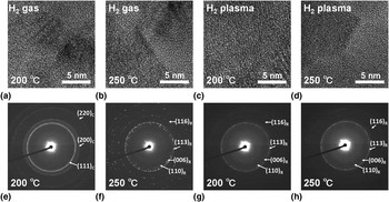
The microstructures of the PCVD films were examined by TEM. Figure 4 shows the representative TEM images and the corresponding electron diffraction patterns for the films deposited at 200 and 250 °C using H2 gas or H2 plasma as the deposition coreactant. All the TEM images show clear lattice fringes, and the electron diffraction patterns show clear diffraction rings, which both indicate that the PCVD films were polycrystalline. Careful analysis of the diffraction patterns was further carried out. We found that, except for the low-temperature (200 °C) H2 gas case [Fig. 4(a)] where the film crystal structure was identified as the fcc Ni (PDF#04-0850), all the other diffraction patterns [Figs. 4(b)–4(d)] matched well with the rhombohedral Ni3C structure (PDF#06-0697), and these findings well agreed with the previous XRD results [Figs. 3(a) and 3(b)].
Representative TEM (a)–(d) images and (e)–(h) the corresponding electron diffraction patterns for the PCVD films deposited on TEM grids at 200 and 250 °C using (a, e, b, f) H2 gas or (c, g, d, h) H2 plasma as the coreactant. The Miller indices labeled in the electron diffraction patterns are based on the fcc Ni structure (subscript “C”) and rhombohedral Ni3C structure (subscript “R”).

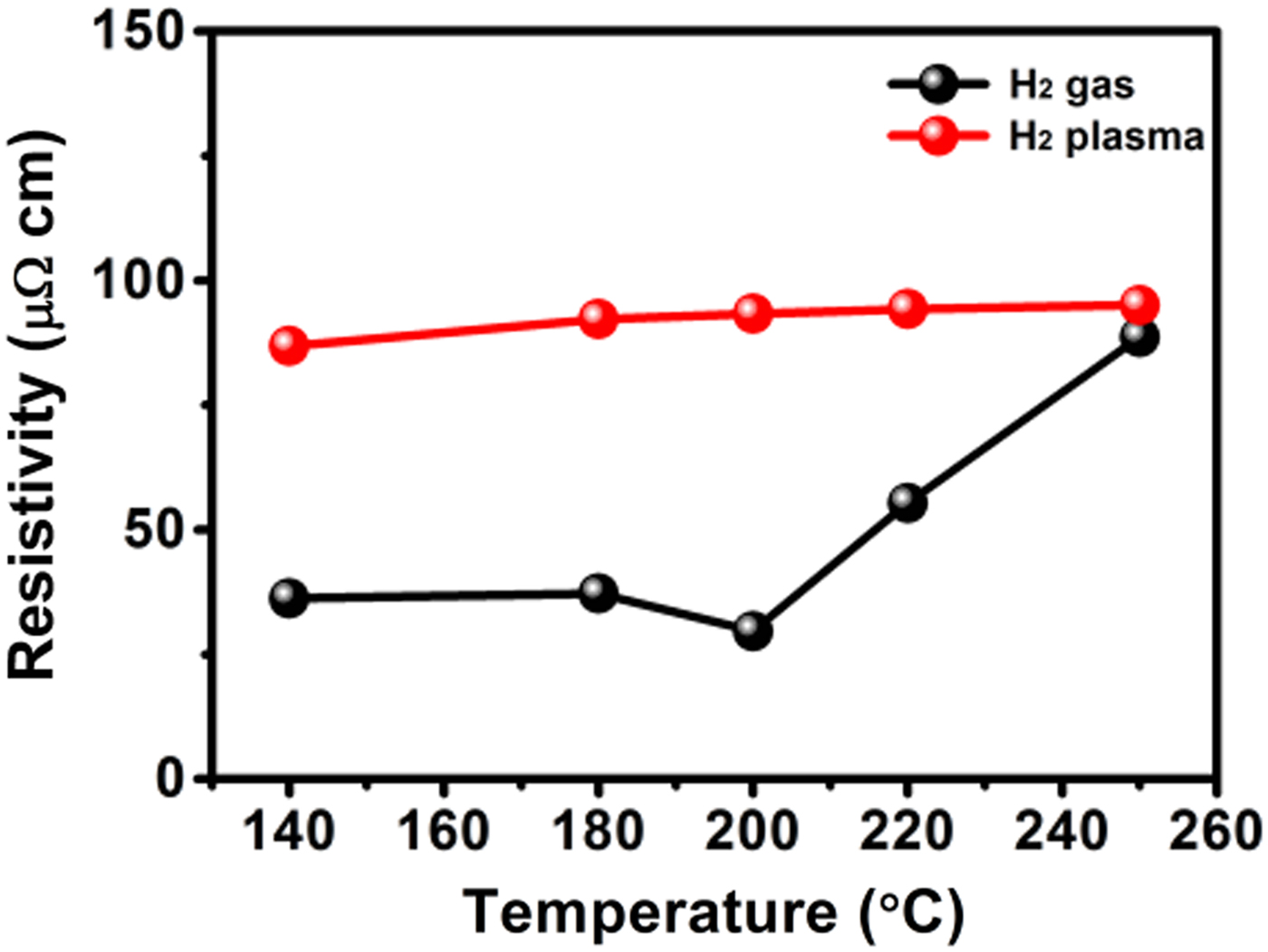
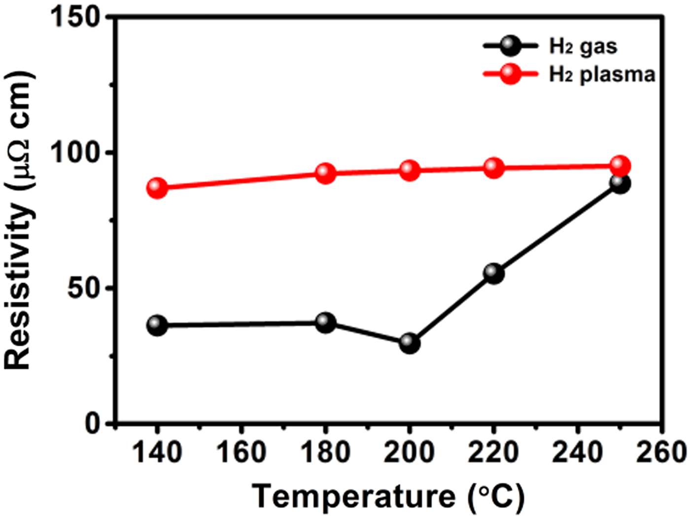
We also characterized the resistivities of the PCVD films. Figure 5 plots the film resistivity with respect to the deposition temperature. For the films deposited with H2 gas, the film resistivity was about 29–37 µΩ cm for the deposition temperature at 140–200 °C, but the resistivity drastically increased as the deposition temperature went beyond 200 °C, reaching 89 µΩ cm for the films deposited at 250 °C. On the other hand, for the films deposited with H2 plasma, the film resistivity showed only a slight increase in temperature from 87 µΩ cm (140 °C) to 95 µΩ cm (250 °C). The variation of the resistivity was correlated to the changes of the C content and crystal phase of the PCVD films: the film resistivity drastically increased as the film crystal phase changed from fcc Ni to rhombohedral Ni3C and the C content increased from low (2.0–3.6 at.%) to high level (≥9.7 at.%). In particular, the lowest number of the resistivities (i.e., 29 µΩ cm) reflects the resistivity of the Ni metal films made by our PCVD process, and this number was fairly close to that of the Ni films made by hot-wire-assisted ALD (27.9 µΩ cm).[ Reference Yuan, Shimizu, Momose and Shimogaki 19 ]
Plot of the resistivities for the films deposited with H2 gas or H2 plasma at various different temperatures.
Conclusions
In summary, we report a new PCVD process for depositing Ni and Ni3C x thin films. The process used bis(1,4-di-tert-butyl-1,3-diazabutadienyl)nickel(II) [i.e., Ni(dad)2] as the metal precursor along with either H2 gas or H2 plasma as the coreactant. The depositions were carried out at various temperatures ranging from 140 to 250 °C, and the deposited films were carefully characterized for various material properties. All the PCVD films were found to be quite pure with the impurity levels of N and O below 0.2 and 1.0 at.%, respectively. The C content and crystal phase of the films depended largely on the deposition conditions. We found that using H2 gas as the coreactant while keeping the deposition temperature ≤200 °C was able to afford fcc-phase Ni metal films with a low C content (2.0–3.6 at.%) and a low electrical resistivity (e.g., 29 µΩ cm), but when the deposition temperature went beyond 220 °C, another phase of rhombohedral Ni3C was formed, accompanying by the increase of the film C content (to 9.7 at.%) and resistivity (to 89 µΩ cm). On the other hand, when H2 plasma was instead used as the coreactant, the deposited films were found to be Ni3C x for all the deposition temperatures (140–250 °C): the films were all in the rhombohedral Ni3C phase and contained a relatively high amount of C (9.7–16.1 at.%) although still lower than that of the stoichiometric Ni3C. The resistivities of these Ni3C x films were also comparatively higher (87–95 µΩ cm). In addition, no sign of nanocrystalline graphite or amorphous carbon was found in the PCVD films as examined by Raman spectroscopy.
Acknowledgments
This work is financially supported by NSFC (grant numbers 11775028 and 51672011), Beijing Municipal Natural Science Foundation (grant no. 4162024), Collaborative Innovation Center of Green Printing & Publishing Technology (grant no. CIDGP15208), Guangdong Natural Science Funds for Distinguished Young Scholar (grant no. 2015A030306036), and Shenzhen Science and Technology Innovation Committee (grant no. JCYJ20170303140959031).