Introduction
Wi-Fi, WLAN, and Bluetooth networks have become essential modes of communication in daily life. Researchers are working extensively in the field to make this communication proficient with improved and cost-effective solutions. Generally, the hardware part of such a communication system includes transmitters, receivers, power amplifiers, repeaters, and control circuit assemblies. The transmitter and receiver are basically an antenna that may be designed with various methodologies (i.e., wire, horn, Yagi, MIMO (Multiple input and multiple output.), etc. [Reference Rana, Sen, Tanjil-Al Mamun, Sheikh, Mahmud and Rahman1–Reference Ren, Hu, Yin and Fan7].) based on the different applications [Reference Balanis8]. The performance and range of communication can be enhanced by utilizing the MIMO or reconfigurable antennas in the setup or by using the antenna repeaters. In the past several years, a number of techniques have been employed to enhance its performance, i.e., reconfigurable intelligent surfaces (RIS), intelligent reflective surfaces (IRS), and frequency-selective surfaces (FSS). However, most of these methodologies require external DC supply or control logic signals to reconfigure the working of such antennas [Reference Rana, Sen, Tanjil-Al Mamun, Sheikh, Mahmud and Rahman1–Reference Narang, Dubey, Negi and Ojha6]. Recently, RIS have been used to enhance or reconfigure various performance parameters of the antenna and MIMO trans-receivers [Reference Huang, Zappone, Alexandropoulos, Debbah and Yuen9–Reference Ahmed, Kumari and Sheoran16]. These parameters include gain, polarization, directionality, etc. These parameters play a vital role in different applications of wireless communication. Generally, RIS works based on reflection, transmission, and absorption modes of operation that can be configured using an electronic switching circuit developed on the RIS. However, IRS is a two-dimensional structure with metallic elements that reflect the incoming waves at a certain design frequency. IRS is generally used as a channel to empower the performance of communication. IRS is designed to achieve several functions in wireless communication, such as coverage extension, interference separation, beamforming, and refining channel statics [Reference Wu, Zhang, Zheng, You and Zhang17–Reference Cui, Zhang and Zhang20]. Whereas, FSS are also the two-dimensional periodic structure of metallic elements on dielectric material that either transmits or reflects the incoming waves at the designed frequency [Reference Raj and Gupta21]. Most of these surfaces are dependent on the control circuitry and the external power supply to work on their intended tasks [Reference Suri and Ranjan Jha22]. This makes these systems complex and costly as well.
This work presents the design and analysis of a cost-effective surface that has the advantages of RIS, i.e., FSS and IRS. The proposed structure is capable of making reflections as well as transmission of the incident waves at the same time and does not require any electronic circuitry or switching to perform the operation. A prototype of the presented surface is designed using the aluminum foil available easily at home. The use of home foil makes it the cheapest intelligent surface. Whereas, the simple design structure gives ease in fabrication. A conceptual working mechanism of the proposed waveguide integrated surface (WIS) is illustrated in Fig. 1(a). This explains that in a dense area where a building is not able to receive the proper signal strength from the source tower, a simple layer of proposed surface can be pasted or designed on the walls of the buildings. This surface predominantly reflects the incident signal in the targeted direction; moreover, the partial transmission allows the signal to communicate inside the building even when it is covered with metallic layers on the walls. Therefore, it can be said that the proposed surface is working as a reflector or repeater up to some extent. Moreover, as compared to regenerative repeaters, this arrangement does not require an external power source and can be utilized for a short range of communication.
(a) Conceptual use of proposed arrangement; (b) Positions of surface with respect to antenna and corresponding radiation pattern.

Further, the designed surface is investigated for reconfiguring the field-directionality of an antenna. To demonstrate the concept, initially, a coplanar microstrip antenna is designed and then associated with the developed surface for field reconfiguration of the designed antenna. A conceptual representation of the arrangement is illustrated in Fig. 1(b). The main advantage of the concept is that the parameters of the antenna can be tuned without affecting the physical structure of that antenna. Moreover, the presented methodology does not require any passive or active components, electronic switching, or an external power supply. This advantage makes it cost-effective and easy to fabricate.
Design and analysis of WIS
The proposed surface is a metallic structure that consists of periodic slot openings integrated into it. The dimensions of this slot are calculated in proportion to the multiple of the operating wavelength of the corrosive waveguide. Therefore, from now on, the structure will be called a WIS. This structure partially transmits the electromagnetic (EM) waves that are coupled through the waveguide slots and reflects the rest of the signal incident upon them. The ratio of reflections and transmissions is maintained by calculating an appropriate dimension of waveguide slots or openings. The dimensions of this integrated waveguide structure are calculated for the dominant mode at the operating frequency of 2.45 GHz by using the waveguide equation [Reference Balanis8].
 \begin{equation}f\, = \,{\text{c /2 W}}\end{equation}
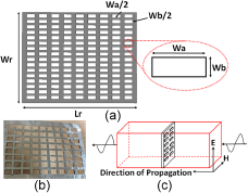
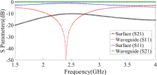
Here, c is the speed of light, f is frequency, and W is the broader dimension of the standard waveguide for the operating frequency. Whereas, the dimension of WIS is related to W as  ${\text{W = 2}}{{\text{W}}_{\text{a}}}{\text{ = 4 }}{{\text{W}}_{\text{b}}}$, where these dimensional parameters Wa and Wb are shown in Fig. 2(a). These parameters are calculated for 2.45 GHz as Wa = 31.25 mm and Wb = 15.625 mm, respectively. The proposed WIS is designed with dimensions of 320 and 265.6 mm and simulated using Ansys’s Electromagnetic Suite to analyze the reflection and transmission parameters. For this measurement, initially, a waveguide is designed and simulated for the operating frequency, then the surface structure is designed and simulated for the measurement of reflection and transmission coefficients. The corrosive EM field with respect to the direction of propagation is shown in Fig. 2(c).
(a) Cross section of the proposed surface; (b) fabricated surface; (c) simulation environment for the proposed surface.

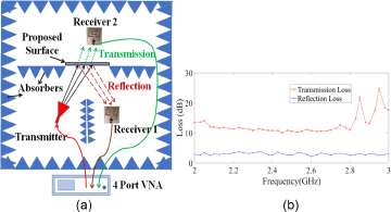
A prototype of WIS is developed with the aluminum foil easily available on the market, as shown in Fig. 2(b). The transmission and reflection from the fabricated surface are measured using the experimental setup given in Fig. 3. A four-port vector network analyzer, R&S ZNA, is connected with the receiving antennas to record the strength of reflected and transmitted signals. A linearly polarized directive antenna (LPDA) (698–2700 MHz) is used as a transmitter in the setup, whereas the proposed microstrip antenna (discussed in the “Reconfiguring the field pattern using WIS” section) is used as both the receivers, as shown in Fig. 4(a). Two identical antennas are fabricated and used for the measurement of the reflection and transmission of the waves. Receiver 1 is used to record the reflections from the surface, whereas receiver 2 is used for recording transmissions through the proposed surface.
Simulated S parameters of the proposed surface.

(a) Experimental setup for measurement of reflection and transmission from the WIS; (b) reflection and transmission graph.

The outcome explains that the proposed WIS only transmits a signal that has a frequency comparable to the dimension of slots. Therefore, the proposed WIS allows partial transmission in the 2.45 GHz band of frequency while reflecting the others completely. Figure 4(b) shows the results for transmission and reflection losses from transmitter to receiver ends, which are 12 and 5 dB, respectively. These values are higher because the designed WIS is a passive-type surface that does not provide any gain to the transmitted or reflected waves.
Reconfiguring the field pattern using WIS
The concept presents a combination of WIS along with the coplanar microstrip antenna to modify the overall performance of that antenna. To validate the concept, initially a coplanar microstrip patch antenna is designed and validated for various performance parameters for the frequency range of mobile communication. In the next step, the WIS is combined with the proposed coplanar microstrip antenna for reconfiguration of its beam directionality.
Design and analysis of antenna
A coplanar microstrip antenna is designed for mobile communication and covers a frequency range of 1.3–5.2 GHz. This range also covers the frequency band of WLAN, Wi-Fi, and Wi-Max applications. Thus, it shows the effective application area of the proposed antenna. This antenna is designed on an FR-4 epoxy substrate with a dielectric constant of 4.4 and a loss tangent factor of 0.02. The proposed antenna is designed for a matched impedance of 50 Ω at the feeding port. The design constraints of the antenna are inspired by the literature [Reference Afruz and Kabir5, Reference Narang, Dubey, Negi and Ojha6]. The dimensions of the proposed antenna are calculated using the equations available in the literature [Reference Balanis8, Reference Gupta23, Reference Mongia, Bahl and Bhartia24] and given in Table 1.
Physical constraints of designed antenna (in mm)

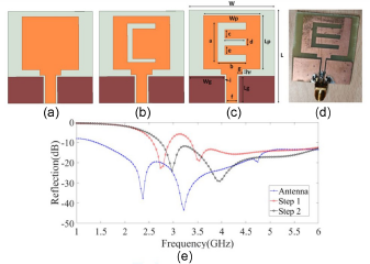
The structure of the antenna is designed, simulated, and optimized in ANSYS’s Electromagnetic Suite software environment. The step–by-step evolution of the proposed antenna and corresponding reflections graphs are given in Fig. 5. The finalized antenna is fabricated in-house using a chemical etching process on a FR-4 substrate with a thickness of 1.5 mm. The comparison of the simulated and measured performance (i.e., reflection and field patterns) of the proposed antenna is given in Fig. 6. The graphs show good agreement between both the simulated and measured performance of the antenna. The designed antenna has a working frequency of 1.3–5.2 GHz with a peak gain of 3.2 dBi. Therefore, this antenna can be used in Wi-Fi, Bluetooth, and WLAN applications.
Cross section of the proposed antenna with design steps (a) step 1; (b) step 2; (c) proposed antenna; (d) fabricated antenna; (e) Reflection graph of antenna for step by step evolution.

Comparison of simulated and measured performance of antenna (a) Reflection graph; (b) Radiation patterns (theta and phi).

Reconfiguring the field directionality of antenna using WIS
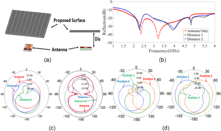
The conceptual representation of the position and functioning of the antenna and WIS is illustrated in Fig. 7(a). This concept is presented to be utilized for varying the field-directivity of the antenna. For this investigation, the WIS is placed at a distance (Dis) from the antenna, and the performance is recorded to compare with the performance of the antenna alone. This distance (Dis) is varied within the near-field region of the antenna and the performance of the combination is observed. Figure 7(b) and (c) gives comparison of antenna parameters with and without the surface for two distances where the directivity changes in a large amount. The measured values of the distance (Dis) are 40 mm (distance 1) and 50 mm (distance 2).The outcome shows that the directionality of the antenna is improved by the proposed combination. Another measurement is also performed for reconfiguring the beam directionality of the antenna at some required angle by placing the WIS along with the antennas illustrated in Fig. 1(b). Here the position of the antenna is fixed; however, the positions of WIS around the antenna reconfigure the directionality as shown in Fig. 7(d). In this measurement, a manual position is applied; however, it can also be motorized to rotate around the antenna to automate the field directionality where require.
Comparison of Antenna performance; (a) S- parameters; (b) radiation pattern (phi and theta) for different values of ‘Dis’; (c) radiation pattern for different distances of WIS w.r.t to antenna; (d) radiation pattern for different positions of WIS w.r.t to antenna.

The fabricated surface, along with the antenna, is used to measure the overall field pattern of the setup. The conceptual experimental setup for this measurement is illustrated in Fig. 8. A reference LPDA is connected to the R&S SMR 40 Signal Generator to generate the RF signal, whereas the surface and antenna are mounted over a rotational stage to rotate the arrangement for measurement of the field patterns. R&S FSH 8 is connected to the antenna designed to record the strength of the received power. All of these arrangements are enclosed with absorbers to remove the external field effect for better measurement accuracy. The radiation patterns (theta and phi) of the antenna are then recorded for every rotational angle of the antenna and WIS arrangement.
Experimental setup for measurement of overall radiation pattern of the antenna in proximity of the WIS.

Figure 9 illustrates the measured performance for reconfiguration of the radiated field of the antenna. The reflection curves show that the combination of the WIS and antenna gives the required reflections within the operating frequency range. Moreover, the measured radiation patterns provide proof of concept for the enhancement of directivity of the antenna.
Measured performance of the fabricated surface along with the antenna; (a) S-parameters; (b) radiation patterns (phi and theta).

Conclusion
The presented WIS is designed for transmission and reflection of electromagnetic signals at 2.4 GHz. Therefore, it gives the possibility of designing a wave coupler (i.e., a power splitter and combiner). Moreover, the surface is investigated for the field reconfiguration of an antenna. This shows that the beam of an antenna can be shaped without any change in the physical structure of the antenna or any external switching circuit. Thus, it is an efficient and cost-effective solution for antenna reconfiguration. Moreover, a simple surface can be designed on the walls of buildings (inside or outside) to divert the range and direction of a Wi-Fi router to control its functionality. The methodology can be very useful in many applications of Wi-Fi, WLAN, and Bluetooth.
Competing interests
Authors do not have any conflict of interest.
Acknowledgements
Acknowledgement: The authors are thankful for CSIR for funding and support to carry out the research work under Project no. “MMP015201” and title “Developing Expertise and Leveraging Terahertz Technology Advancement in CSIR (DELTA)”.