I. INTRODUCTION
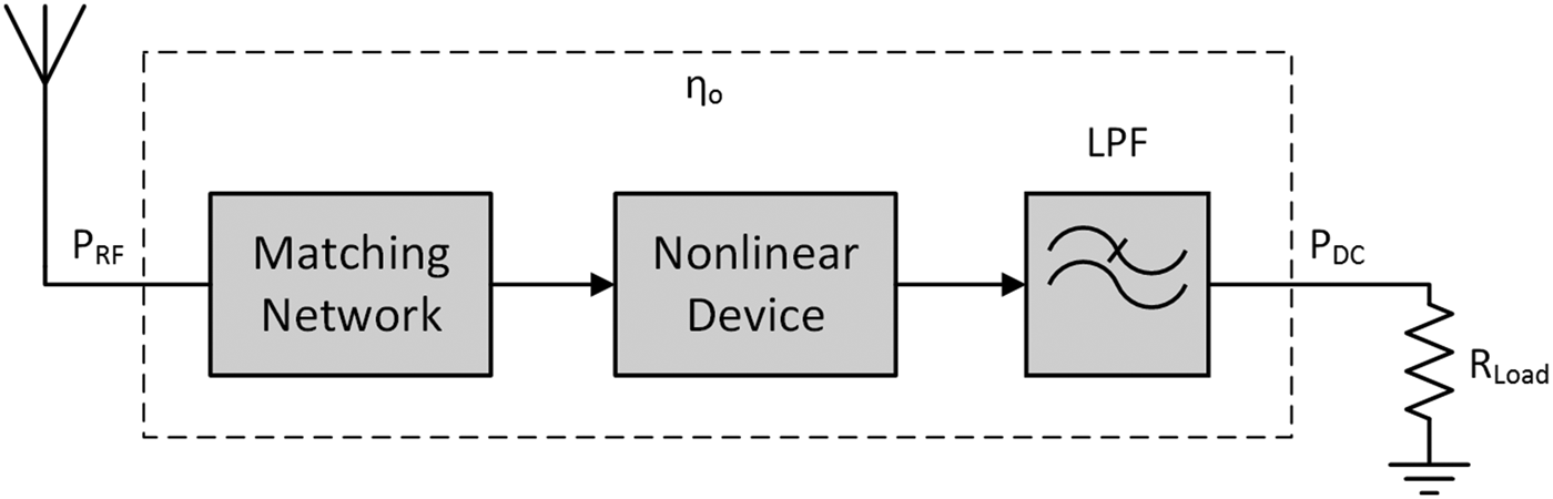
Radio-frequency energy harvesting (RF EH) consists in capturing electromagnetic power from RF signals available in the surroundings and converting it into power that can be reused. The increased number of sources radiating considerable amounts of power (e.g. cell phone towers, broadcast television signals) induces a global spread of the available electromagnetic fields in the environment. Therefore, RF EH constitutes a very promising way to power up devices, such as low-power sensors, avoiding the need for battery replacement, turning them self-sustained, and reducing the costs. The RF EH system is an antenna combined with a rectifier, commonly known as rectenna and introduced by W.C. Brown in the early 1960s [1]. A typically block diagram is presented in Fig. 1. The rectifier elements are the matching network, the non-linear device(s), and the low-pass filter.
RF EH system block diagram.

The RF-to-DC conversion efficiency (η o) is the rectifier key role and it is defined by equation (1), where P RF is the incident RF power, P DC the output DC power, V DC the output voltage, and R Load the load resistance.
 $$\eta _{\rm o} = \displaystyle{{P_{DC}} \over {P_{RF}}} = \displaystyle{{V_{DC}^2} \over {P_{RF} \times R_{Load}}}.$$
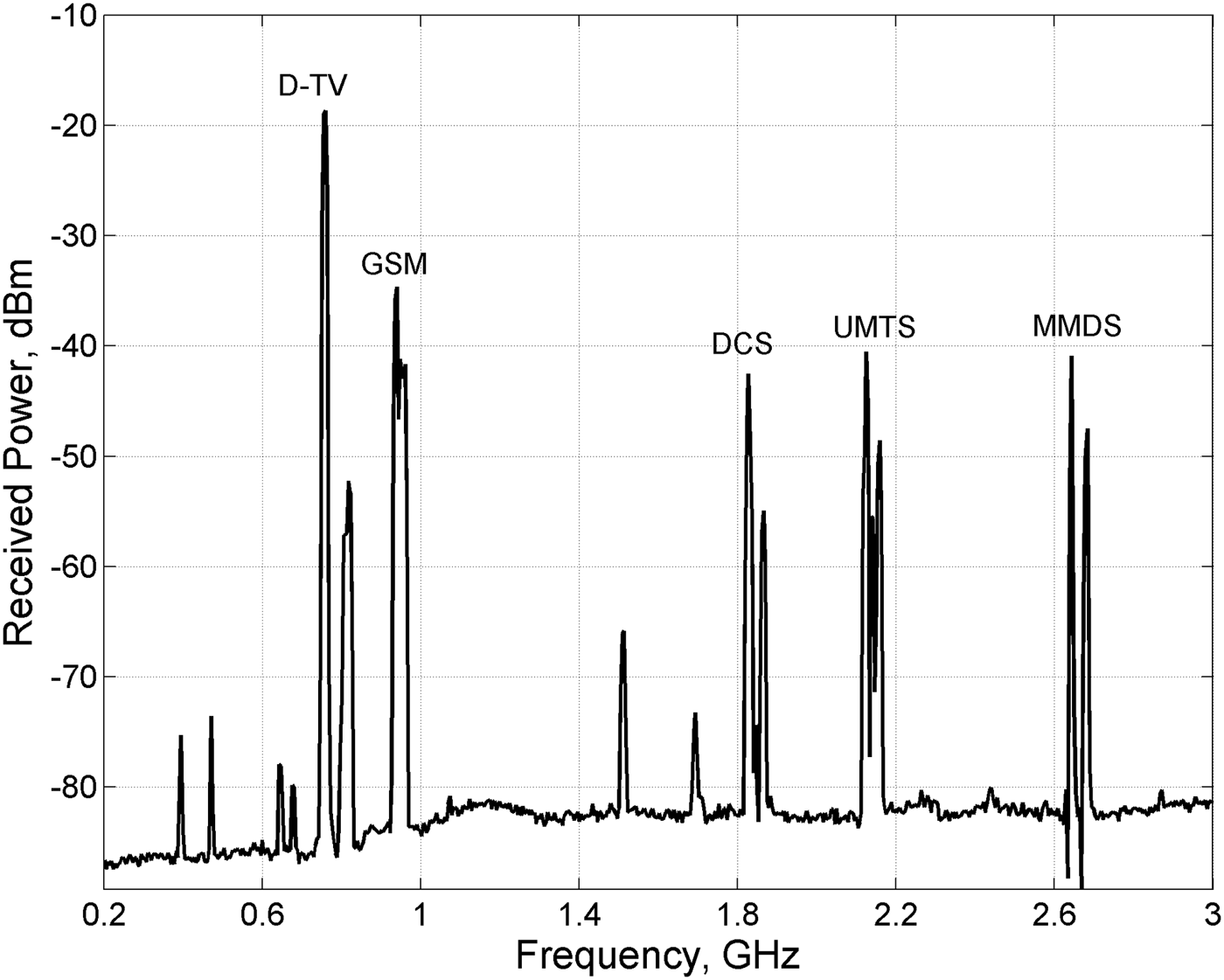
The power spectrum from 200 MHz to 3 GHz in the city of Aveiro (Portugal) is presented in Fig. 2, measured with a Rohde & Schwarz FSH8 spectrum analyzer and a wideband HL300 antenna. It is possible to identify the Portuguese Digital Television (D-TV), the Global System for Mobile Communications, the Universal Mobile Telecommunications System, and the Multichannel Multipoint Distribution Service spectra's. Nevertheless, D-TV exhibits the higher power density, explained by the proximity to a D-TV transmitter that radiates 3200 W. Around all the countries there are 231 D-TV transmitters radiating at channel 56 (750–758 MHz), whose effective radiated power goes from 6.5 W up to 8600 W [2]. Thus, D-TV spectrum seems suitable to be used as RF source for EH applications.
Power spectrum at the city of Aveiro.
Regarding the rectifier circuit, the non-linear element assumes a big importance on the power conversion efficiency and should be carefully chosen to satisfy the project demands. Schottky diode is employed in this work due to its typically low cut-in voltage and fast switching capabilities. There are many configurations defined according to the number of non-linear elements and their position. Simple rectifier solutions, such as half-wave rectifiers with one or two non-linear devices, have shown improved efficiencies for low incident power levels than complex structures, such as bridge rectifiers [Reference Mabrouki, Latrach and Sayegh3, Reference Marian, Allard, Vollaire and Verdier4]. Despite EH has been in vogue in the last years, only a few works present considerable efficiencies below 0 dBm. For instance, in [Reference Collado and Georgiadis5, Reference Franciscatto and Freitas6] were reported efficiencies of 40% at −11.5 dBm and 60% at −10 dBm, respectively. In [Reference Vyas, Cook, Kawahara and Tentzeris7] is proposed an EH system that also uses the D-TV signal as RF source. Nevertheless, the rectifier is composed by several stages that result in a high output voltage but in a low efficiency. Therefore, efficiency improvements at low incident power levels are still an open issue.
This work presents a low-cost voltage-doubler rectifier that can achieve 63% efficiency at −10.5 dBm with the D-TV signal excitation. Also, a single-shunt and a single-series rectifier configuration are proposed and both have shown good performance at low input power levels, emphasizing that the rectifiers with low number of non-linear devices are suitable for EH. Moreover, it is proven in this paper the efficiency improvement obtained with the D-TV signal in comparison with the sine-wave one.
The paper is divided into the following sections: Section II focuses on the rectifier circuit, where the three implemented circuits, the respective design steps and the considerations taken into account are presented. Section III shows the proposed antenna. Section IV validates the EH system with measurements on site, and finally, in Section V are presented the main conclusions.
II. RECTIFIER CIRCUIT
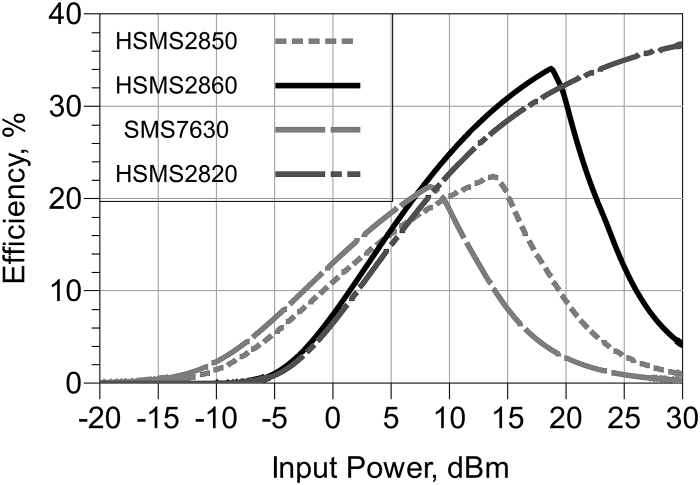
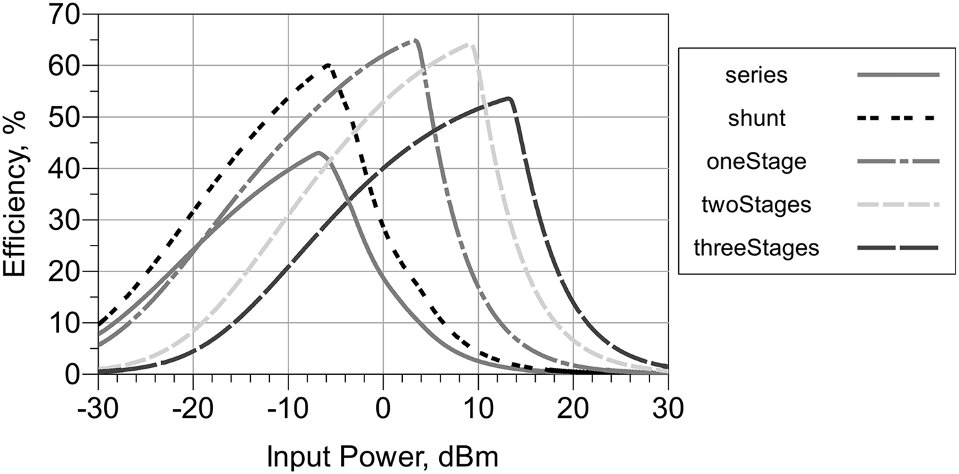
To improve the power conversion efficiency, the Schottky diode and the rectifier topology are chosen based on simulation results. According to Fig. 3, obtained by changing the commercial Schottky diode in a single-series diode rectifier, both SMS7630 [8] and HSMS-2850 [9] show a higher sensitivity. Similarly, the performance of different rectifier configurations is compared. As the input reflection coefficient can significantly change between each configuration, it was provided a matching network, optimized to −10 dBm, in order to obtain conclusions at lower input power levels. The results are shown in Fig. 4 for a single-series, single-shunt, and three voltage multipliers (1, 2, and 3-stage) and indicate that configurations with a low number of non-linear devices boost the efficiency at lower input power levels.
Power conversion efficiency employing different diodes.
Power conversion efficiency for different rectifier topologies.
Hence, a single-series, a single-shunt, and a voltage-doubler rectifier configuration are designed. Both single-shunt and single-series rectifiers employ the SMS7630 Schottky diode. For the voltage doubler the choice is the HSMS-2852, that is a package with two HSMS-2850 diodes in series. Consequently, the mounting process is simplified and the losses and extra parasitic's of having two different packages are reduced. Moreover, the rectifiers are optimized to obtain maximum efficiency within D-TV channel 56 and to −10 dBm of input power.
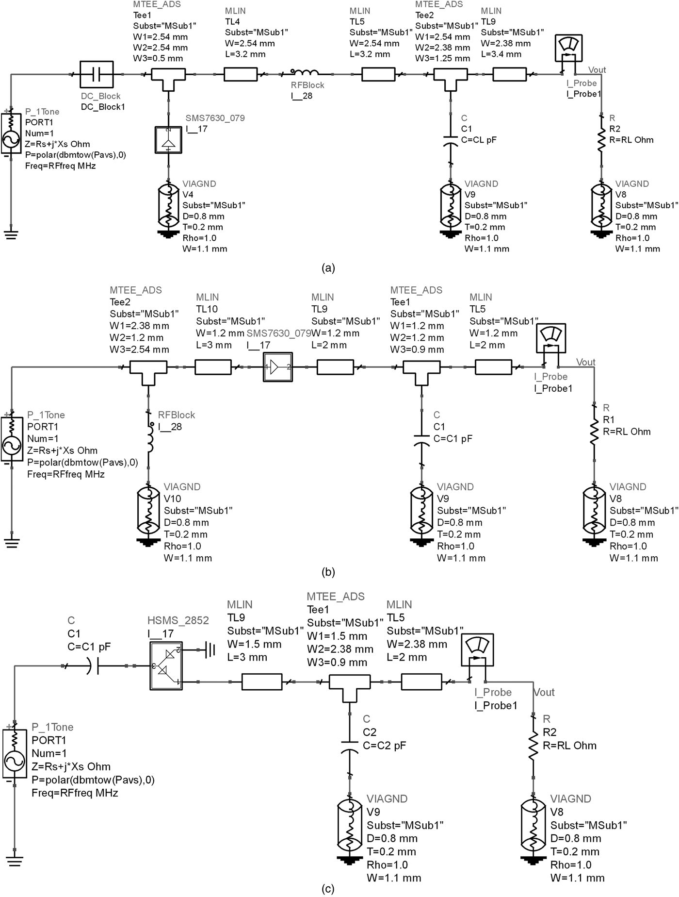
The single-shunt rectifier circuit is presented in Fig. 5(a). The choke (RFBlock) prevents the RF signal from reaching the load. The capacitor (CL) was included to reduce the output voltage ripple. Regarding the single-series rectifier simulation schematic, presented in Fig. 5(b), it was verified that the inclusion of a DC path to ground at the Schottky diode anode enhances the efficiency. Finally, the voltage-doubler design circuit is shown in Fig. 5(c).
Simulation schematics. (a) Single-shunt diode. (b) Single-series diode. (c) Voltage-doubler.
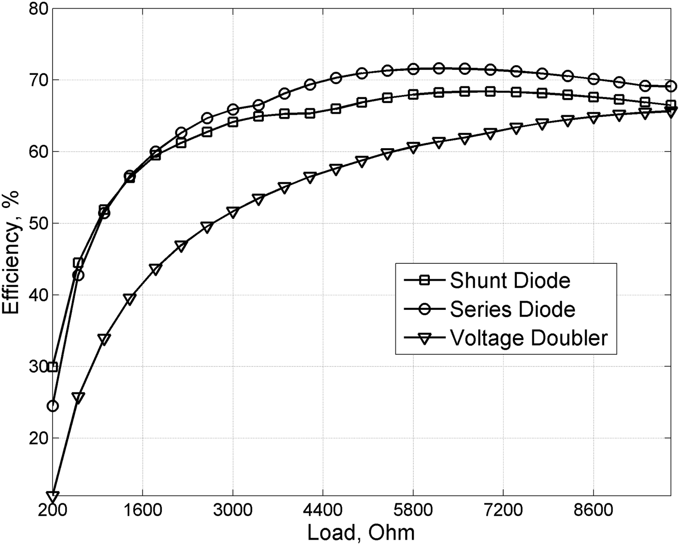
The expected maximum efficiency for the three configurations as function of the load (R L) is presented in Fig. 6. For each R L value, the maximum efficiency with the optimal input impedance was determined through source pull simulations. However, according to source pull efficiency curves for the ideal R L value, small deviations around the ideal input impedance produce a high decrease in the efficiency. Therefore, the impedance matching would require a good agreement between simulations and measurements. For lower R L values, the input impedance misalignment yields a lower efficiency variation. Thus, the load for each rectifier is maintained below the ideal one, whose values are 3300, 3900 and 7500 Ω for the single-shunt, single-series, and voltage-doubler, respectively. The capacitor value is set to 100 pF for the three rectifiers.
Maximum efficiency vs. load for each rectifier.
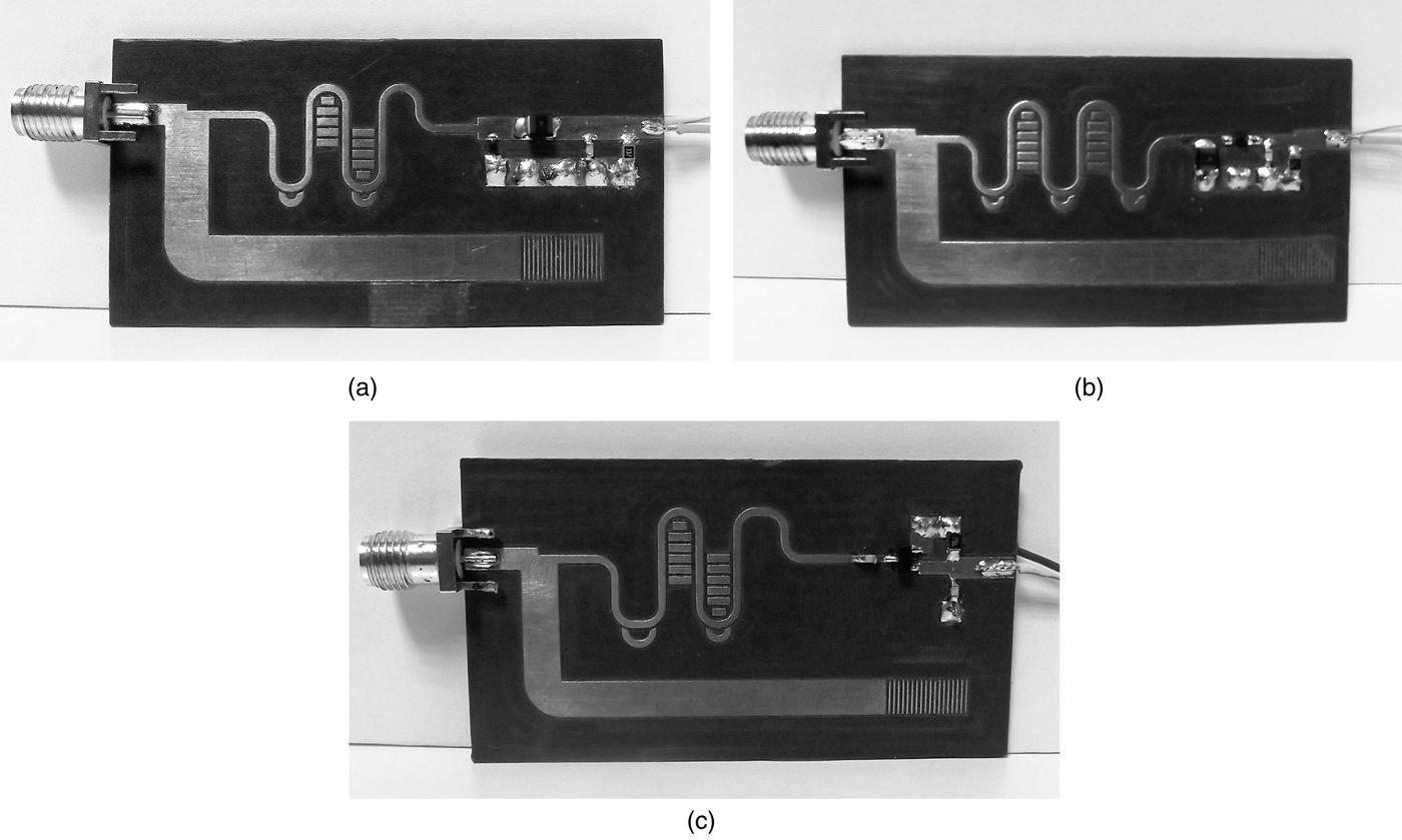
To provide the impedance matching between the 50 Ω source impedance and the rectifier input one, a shunt open stub followed by a line is used. As the ideal impedance to be presented to the input that maximizes efficiency is closer for each rectifier, the resulting matching networks become similar. To reduce the occupied area and, consequently, the cost, the matching network was compressed through the introduction of curves in the line and open stub. Finally, in order to obtain a more accurate behavior of the designed circuits, electromagnetic simulation is performed and a slight mismatch in comparison with the schematic simulation is verified. As consequence, small changes in the matching elements are conducted. The implemented rectifier circuits are presented in Fig. 7.
Implemented rectifier circuits. (a) Single-shunt diode. (b) Single-series diode. (c) Voltage-doubler.
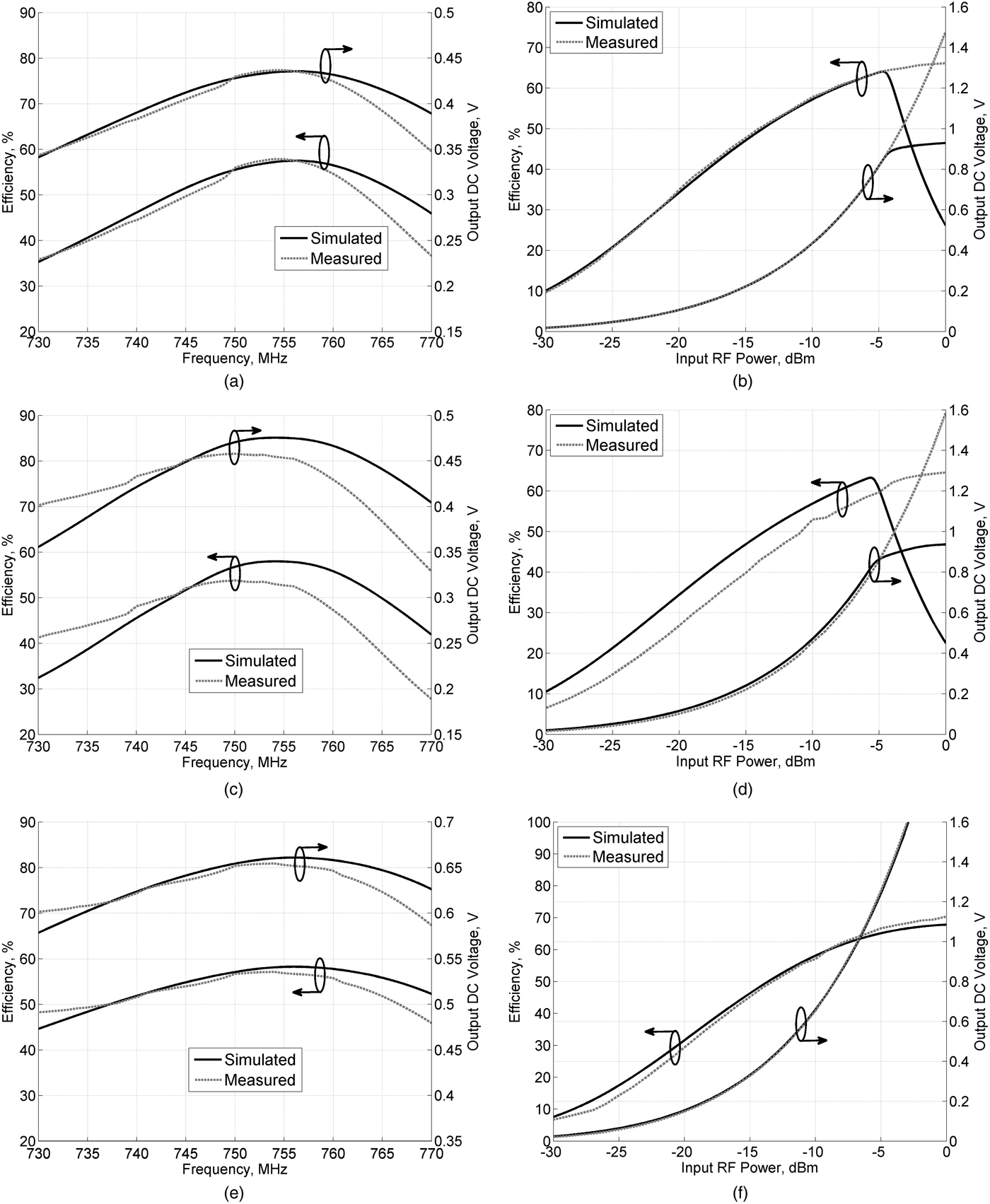
The rectifiers’ response to a single-tone excitation is shown in Fig. 8. The output DC voltage and efficiency are plotted for both frequency and input power sweeps. In the frequency sweep, the input power is kept as −10 dBm and in the power sweep the frequency is set to 754 MHz. The single-shunt rectifier presents the higher maximum efficiency at −10 dBm (about 58%). Nevertheless, the voltage-doubler has shown about 57% of maximum efficiency at −10 dBm and, as expected, it reaches higher output voltage levels. The single-series has shown an increased misalignment between measurements and simulations results, resulting in a lower and frequency-shifted maximum efficiency. Despite the rectifiers have been optimized to collect the spectrum from the D-TV 56 channel, the results presented in Fig. 8 indicate that they are able to operate outside this band. Moreover, these results point out that the designed rectifiers have a high sensitivity. For instance, the single-shunt diode presents 10% efficiency at −30 dBm.
Rectifiers performance with sine-wave excitation. (a) Single-shunt diode frequency response (P RF = −10 dBm). (b) Single-shunt diode input power response (RF freq = 754 MHz). (c) Single-series diode frequency response (P RF = −10 dBm). (d) Single-series diode input power response (RF freq = 754 MHz). (Voltage-doubler frequency response (P RF = −10 dBm)). (e) Voltage-doubler input power response (RF freq = 754 MHz).
III. RECEIVER ANTENNA
The receiver antenna pretends to be low cost, should have high gain and be able to cover the D-TV 56 channel. The first approach was to develop a microstrip patch antenna due to its low profile and low-cost fabrication, based in equations presented in [Reference Balanis10]. The dielectric substrate is used the FR-4 with a dielectric constant (ɛ r) of 4.3, a tangent loss (tan δ) of 0.019, and a thickness (h) of 1.6 mm. However, microstrip patch antennas typically exhibit narrow BW and due to the small thickness of the substrate compared with the wavelength (λ o = 400 mm) the BW becomes even more constrained, as verified. To obtain an antenna with the required BW using the referred substrate is quite challenging and demands exchanges in the basic patch. Additional parasitic elements [Reference Parmar, Makwana and Jajal11], slots [Reference Sharma, Katariya and Meena12] and stacked elements [Reference Chung and Mohan13, Reference Chung and Mohan14] are commonly used to increase the patch antenna BW.
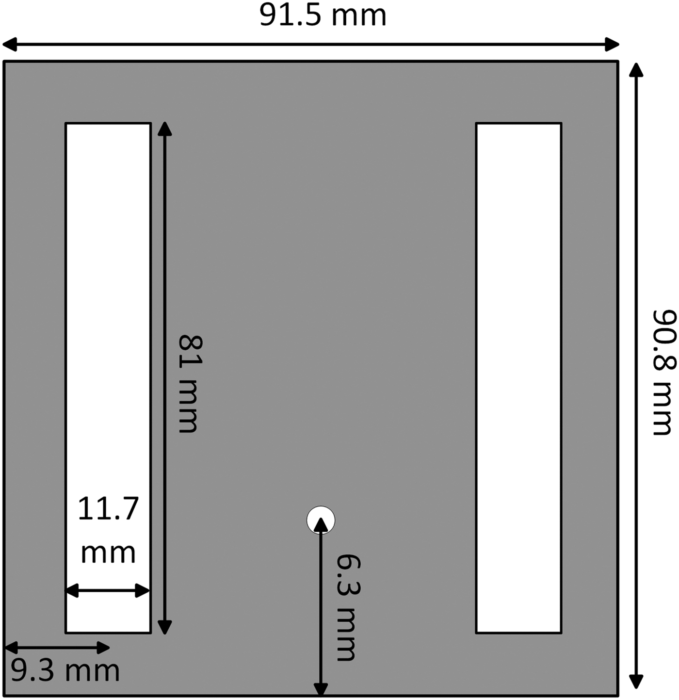
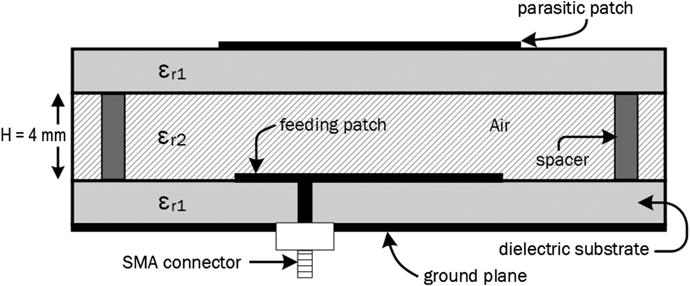
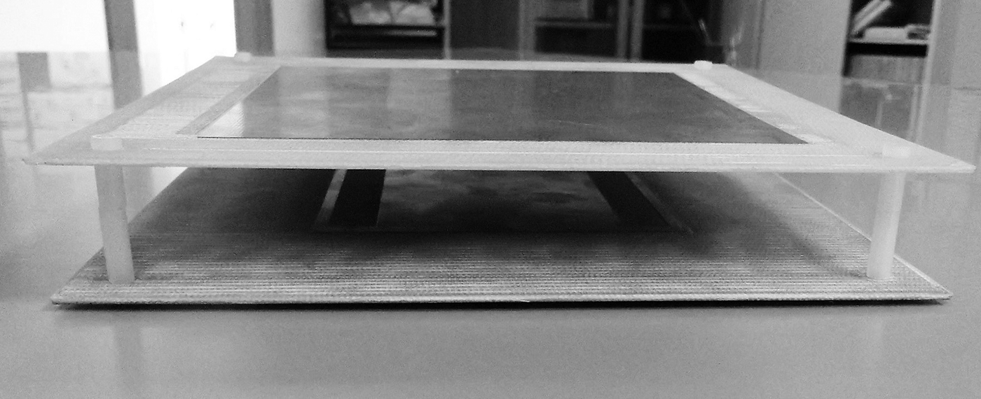
Hence, two rectangular slots were introduced, as exemplified in Fig. 9. They will change the patch inductance and, with careful design, it is possible to increase the antenna BW [Reference Munir, Petrus and Nusantara15]. The BW improvement was enough to cover the entire channel 56; however, the gain remains unchanged with this configuration, which is highly desired to improve the EH system performance. To increase both gain and BW, a parasitic element is stacked to the slotted microstrip patch (feeding patch), as shown in Fig. 10. The feeding and parasitic patches are separated by an air-gap space H, highly dependent on the wavelength and electrical characteristics of the used substrates. The air gap is set to 4 mm. Moreover, the length and width of the parasitic patch also have an influence in the BW, resulting in 1.45 times the length and width of the feeding patch, respectively, through optimization. The remaining dimensions of the final proposed antenna that led to the best performance are presented in Fig. 9 and the implemented antenna is shown in Fig. 11.
Slotted patch configuration.
Parasitic stacked patch configuration.
Implemented antenna.
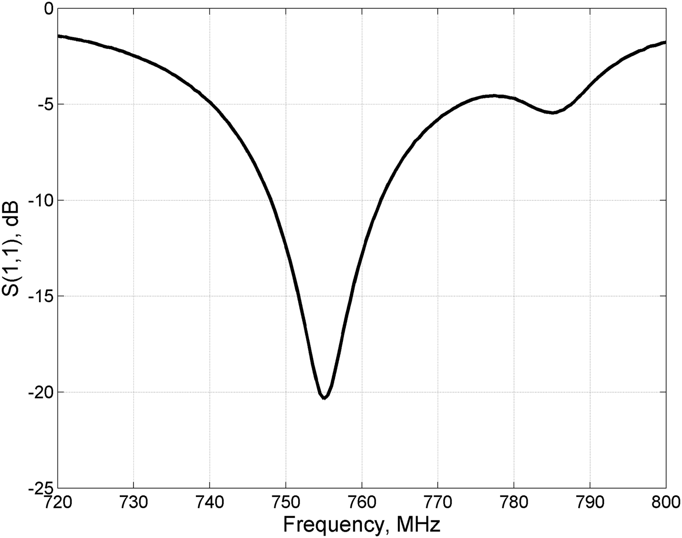
The input reflection coefficient of the implemented antenna is presented in Fig. 12, and dictates a BW about 14.5 MHz, which is three times the expected one with the basic microstrip patch through simulations. Although the gain was not measured, simulations predict an increase from 3.1 dBi (basic and slot configurations) to 6.9 dBi (stacked slot patch). Therefore, the proposed antenna is able to collect all the spectra from the Portuguese D-TV channel 56 efficiently and results in a higher gain antenna, which increases the overall performance of the EH system.
Measured input reflection coefficient.
IV. SYSTEM VALIDATION
The EH system validation is made with measurements around the D-TV Aveiro center transmitter, using the developed receiver antenna connected to one of the rectifiers. As proof of concept, these measurements are made only with the voltage-doubler circuit, due to higher output voltage levels obtained with the single-tone excitation, without jeopardizing the efficiency, as shown in Section II.
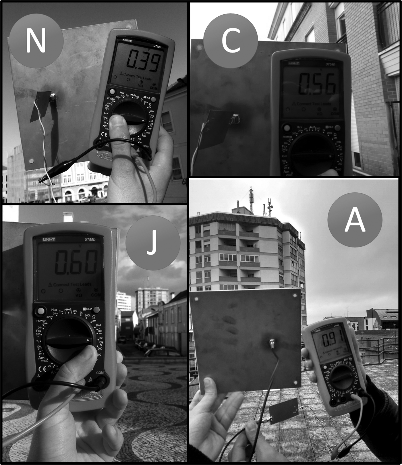
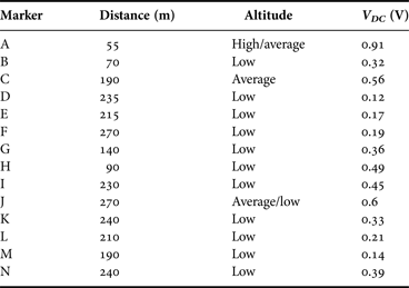
The map presented in Fig. 13 marks the locations from A to L where the measurements took place and the D-TV transmitter (Tx). The output DC voltages obtained on the site are presented in Table 1, as well the distance of each marker to the transmitter and an empirical estimation of the altitude relative to the transmitter antenna. Moreover, all the measurements were made with line of sight between the EH system and the transmitter. Otherwise, the output DC voltage obtained is insignificant. To prove the results shown in Table 1, Fig. 14 presents the measurements made at four of the different markers.
Measurements locations around Aveiro D-TV transmitter (Tx).
Output DC voltage at four different locations.
Aveiro city measurements results.
Briefly analyzing Table 1 results, the higher DC voltage was obtained at marker A (0.91 V), due to its closer proximity to the D-TV transmitter. Both F and J markers are located at around 270 m away from the transmitter. However, the output DC voltage obtained in each one is quite different: 0.19 V at F and 0.6 V at J. The slightly higher altitude of marker J or even the possibility of the transmitter antennas not radiate uniformly in all directions could justify the observed deviation.
Despite not being particularly analyzed, reliable performances were also obtained in the remaining markers, where distance and altitude have also shown to produce a large impact in the output voltage. Moreover, at further distances it is still expected to obtain considerable output voltages, especially for a certain altitude.
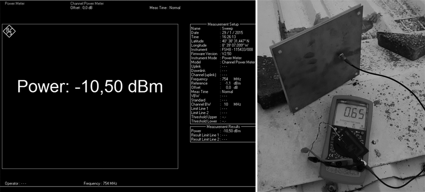
Regarding the efficiency, the received power was measured with the Spectrum Analyzer and then the rectifier was connected to measure the output DC voltage. As shown in Fig. 14, the total power received from channel 56 was −10.5 dBm and the respective output DC voltage was 0.65 V. According to (1), the resulting power conversion efficiency is 63.2% and it corresponds to an increment about 7% the obtained with the single-tone excitation at the same input power. This is a consequence of the higher peak-to-average ratio of the D-TV signal relative to the sine-wave, which allows the diode non-linearities to respond in a more efficient way [Reference Boaventura, Collado, Georgiadis and Borges Carvalho16].
Power received by the antenna (left) and output DC voltage at the voltage-doubler (right).
V. CONCLUSION
The three rectifier circuits proposed along this work were designed to properly operate under weak power signals through a careful analysis of their elements. These circuits have shown a high sensitivity and considerable efficiency levels at low-power conditions. A good agreement between simulations and measurements results was also verified.
The measurements on site, using the developed antenna connected to the voltage-doubler, proved the feasibility of the EH system. Also, the efficiency improvements verified with the D-TV signal excitation relative to the sine-wave one is a positive result to take from the measurements. Hence, promising results to use D-TV as RF source to power low-power devices were demonstrated.
ACKNOWLEDGEMENTS
None.
FINANCIAL SUPPORT
This work is funded by FCT through national funds under the project CREATION EXCL/EEI-TEL/0067/2012.
STATEMENT OF INTEREST
None.
Tiago Moura received the Master degree in Electronics and Telecommunications Engineering from the University of Aveiro. In 2014, he joined the Institute of Telecommunications as a researcher, where its main activities include the design and measurement of MMICs for space applications. His main research interests are energy harvesting, design of non-linear devices, and WPT.
Nuno Borges de Carvalho received the Ph.D. degree in Electronics and Telecommunications Engineering from the University of Aveiro in 2000. He is currently a Full Professor, IEEE Fellow, and a Senior Research Scientist with the Institute of Telecommunications, University of Aveiro. He co-authored Intermodulation in Microwave and Wireless Circuits (Artech House, 2003). He has been a reviewer and author of over 100 papers in magazines and conferences. He is an Associate Editor for the Cambridge Wireless Power Transfer Journal. He co-holds four patents. His main research interests include software-defined radio front-ends, WPT, non-linear distortion analysis in microwave/wireless circuits and systems, and measurement of non-linear phenomena. He is an associate editor for the IEEE Transactions on Microwave Theory and Techniques and IEEE Microwave Magazine. Dr. Borges Carvalho is the chair of the IEEE MTT-11 Technical Committee. He is the chair of the URSI-Portugal Metrology Group.
Pedro Pinho was born in Vale de Cambra, Portugal in 1974. He received the Master's degree in Electronics and Telecommunications Engineering and the Ph.D. degree from the University of Aveiro in 1997, 2000, and 2004, respectively. He is currently a Professor Adjunto at the Department of Electrical Telecommunications and Computers Engineering in Instituto Superior de Engenharia de Lisboa, in Instituto Politécnico de Lisboa, and a Senior Member of the research staff at the Institute of Telecommunications. His current research interest is in antennas for location systems, reconfigurable antennas, and antenna design for passive sensors in non-conventional materials. He has authored or co-authored more than 100 research papers in conferences and international journals and book chapters.