I. INTRODUCTION
Electronics based on complementary metal–oxide–semiconductor (CMOS) transistors and their scaling according to Moore's law Reference Moore1 has been the foundation of the information technology revolution in the past 45 years. It is poised to continue scaling for at least the next 15 years as outlined in the International Technology Roadmap for Semiconductors (ITRS). 2 In the last 10 years, significant research effort has been devoted to find alternative devices that can perform logic operations, see e.g., Ref. Reference Bernstein, Cavin, Porod, Seabaugh and Welser3. Although it is not likely that any beyond-CMOS device will be able to replace CMOS, such devices are targeted for attributes that supplement those of CMOS. Among these attributes are low-power dissipation and nonvolatility. One of the classes of beyond-CMOS devices that possesses these valuable characteristics are spintronic devices, Reference Zutic, Fabian and Das Sarma4,Reference Nikonov and Bourianoff5 i.e., the ones based on switching of nanomagnets. To compare beyond-CMOS devices and to identify more promising options, a uniform methodology of their benchmarking has been developed. Reference Nikonov and Young6,Reference Nikonov and Young7 Since its publication, this methodology achieved good reception and has been adopted by multiple research groups. One of the conclusions of that study was that spintronic circuits, based on switching of magnetization by spin torque (ST) (see Ref. Reference Locatelli, Cros and Grollier8 for a review), are significantly slower and more energy-demanding compared with CMOS. Over the last few years, magnetoelectric (ME) switching has been demonstrated to make significant impact in enabling a difference by enabling lower energy switching, and it therefore seems attractive to explore further for use in spintronic devices and circuits.
The ME effect in general has been the subject of several review papers. Reference Fiebig9–Reference Nan, Bichurin, Dong and Viehland12 Based on this effect, various ME devices (mostly memory) have been demonstrated, e.g., Refs. Reference Gajek, Bibes, Fusil, Bouzehouane, Fontcuberta, Barthelemy and Fert13–Reference Tiercelin, Dusch, Klimov, Giordano, Preobrazhensky and Pernod15. To advance the field, we aim to compare both experimentally demonstrated and required parameters of ME switching and to estimate the performance of simple logic circuits based on ME devices.
In this study, we perform an in-depth study of ME materials underpinning spintronics devices and update their benchmarking with the new inputs. We start with a review of experiments on ME switching. We distinguish 3 mechanisms for such switching and explain the physical phenomena involved. We place the results of the analysis into the common benchmarking for comparison, considering the applied electric field and the obtained ME field. We perform micromagnetic simulation of ME switching of nanomagnets and of interconnects that are based on domain wall motion. The values of the required ME field and switching delay are then used in benchmarks of devices based on ME switching and for comparison of various switching mechanisms for spintronic devices. We conclude with the discussion of the updated benchmarks.
II. ME SWITCHING EXPERIMENTS
Switching of magnetization by ST is controlled by the current passed through the ferromagnet for most of the time necessary for switching. However, ME switching of magnetization is controlled by voltage applied to a stack of dielectric materials. This aspect brings about the main advantage of ME switching. Although certain current is needed to charge a capacitor to create the voltage, it typically occurs for a time much shorter than the magnetization switching delay. Moreover, the charge transferred in ME switching is much smaller than that in ST or other types of current-controlled switching.
To explain the benchmarking estimates we performed, we need to review the fundamentals of the ME effect. Reference Fiebig9 Its essence is a contribution of the magnetic field to electric displacement and of the electric field to the magnetic induction, as follows:
 $$D = \varepsilon {\varepsilon _0}E + \alpha H\quad ,$$
 $$B = \mu {\mu _0}H + \alpha E\quad .$$
The coupling coefficient for direct and converse ME effects are defined from the above Eqs. (1) and (2).
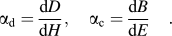 $${\alpha _{\rm{d}}} = {{{\rm{d}}D} \over {{\rm{d}}H}},\quad {\alpha _{\rm{c}}} = {{{\rm{d}}B} \over {{\rm{d}}E}}\quad .$$
Theoretically, these coefficients should be the same; however, in practice, the direct coefficient proves to be 2–4 times larger. The ME coefficient α has the units of s/m and the characteristic value of the inverse speed of light. The ME effect is not necessarily linear, or, in other words, the ME coefficient can depend on the magnitude of applied fields. We will utilize the term ‘ME field’ for the contribution to Eq. (2) from the ME effect.
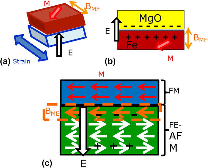
Although there are some materials in which the electric and magnetic characteristics are coupled, most practical demonstrations involve composite materials: a layer of a ferromagnetic (FM) material undergoing switching and an adjacent layer of a ME material (in most cases an oxide) interacting with the FM material at the interface. We will distinguish the following mechanisms of switching, depicted in Fig. 1.
Layer schemes for 3 types of ME effect: (a) magnetostrictive; (b) surface anisotropy; (c) exchange bias.
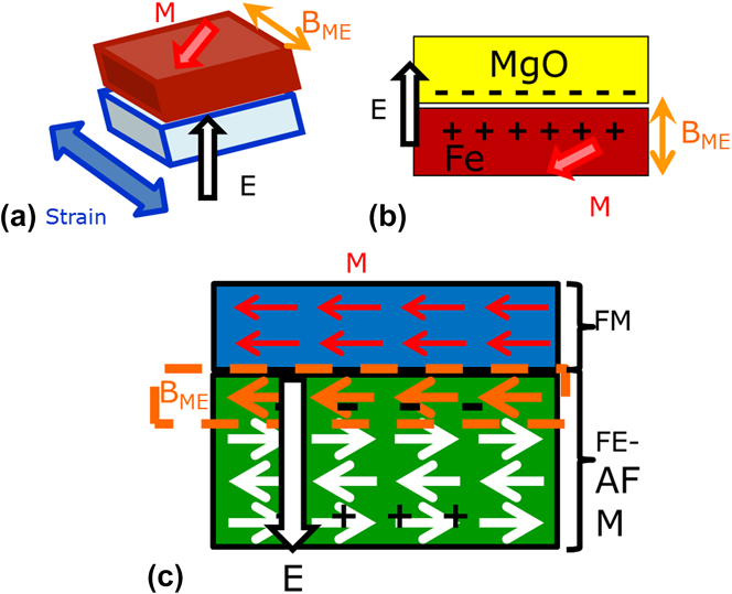
Magnetostrictive effect (‘ms’) [Fig. 1(a)]. In this case, an electric field is applied to a layer of a piezoelectric material, and it creates a strain in it. Reference Zhai, Xing, Dong, Li and Viehland11 The stress from the piezoelectric layer, such as BTO (BaTiO3), is transferred to the FM layer and changes the magneto-crystalline anisotropy in it; this change is called ‘magnetostriction’. The change can be large enough to switch the direction of the easy axis of magnetization by 90°. In a few cases, the piezoelectric material is also a ferroelectric, i.e., it has spontaneous polarization even in the absence of an external electric field. Then, the polarization and strain in such a material will exhibit hysteresis. In general, the polarization and strain vary with the applied electric field, and thus the ME field can be increased.
Surface anisotropy effect (‘su’) [Fig. 1(b)]. If voltage is applied to a thin layer of oxide, typically MgO, charge density is varied at the interface of the oxide and the FM layer. Reference Wang, Li, Hageman and Chien16 As a result, surface magnetic anisotropy of the FM layer is changed. Note that surface anisotropy is determined by the interface. However, the value of the ME field in an experiment is related to the specific thickness of the FM layer. For a different thickness, the ME field needs to be rescaled.
Exchange bias effect (‘eb’) [Fig. 1(c)]. More generally, exchange bias Reference Cheong and Mostovoy10 is an interaction of spins at the interface of 2 materials. The spins at the surface of the ME material comprise a net polarization, which biases the hysteresis loop of the FM material, akin to an effective ME field. Typically, the ME material is an antiferromagnet. For the switching case, we are interested in the electrically switchable exchange bias. It can occur if the spin polarization is coupled to the electric polarization in the ME material; then by switching one, the other can be switched. There are cases when the ME material has a spontaneous electric polarization, such as BFO (BiFeO3). Reference Chiu, Martin, Holcomb, Gajek, Han, He, Balke, Yang, Lee, Hu, Zhan, Yang, Fraile-Rodríguez, Scholl, Wang and Ramesh17 Then, it is classified as multiferroic, i.e., a material having both electric and magnetic order. In other cases, such as Cr2O3, the ME material does not have spontaneous electric polarization and is not a multiferroic material. Both types of materials can be used for switching.
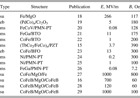
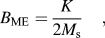
In the following, we perform the analysis of several experimental reports of ME switching. The list of the experiments is not claimed to be exhaustive; rather, it aims to provide a few representative cases. We summarize the results of these experiments in Table I, where the type of the effect, the structure of FM and ME layers, and the references are listed. Also, the applied electric field is listed, and the effective ME field is calculated. In different cases, it is obtained from the change of the coercive magnetic field, shift of the magnetic hysteresis loop, or calculated from the inferred change of the magnetic anisotropy energy per unit volume, K, as follows
 $${B_{{\rm{ME}}}} = {K \over {2{M_{\rm{s}}}}}\quad ,$$
where M s is the saturation magnetization in the FM layer.
Summary of selected experiments on ME switching. Type: ‘su’ = surface anisotropy, ‘eb’ = exchange bias, ‘ms’ = magnetostrictive. E = applied electric field, B = produced ME field.

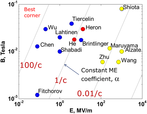
From Table I and Fig. 2, one can make the following observations about the mechanisms of ME switching. The surface anisotropy effect has the smallest ME coefficients (from 10−3/c to 0.1/c). It, therefore, requires the largest electric field to achieve modest values of the ME field. However, it also comprises the observation of the highest ME field. Reference Shiota, Nozaki, Bonell, Murakami, Shinjo and Suzuki27 The magnetostrictive effect has the largest ME coefficients (from 1/c to 100/c). It can therefore achieve large values of the ME field with only a small electric field. This fact is extremely important for low-power operation of devices because the switching energy is proportional to the square of voltage. The exchange bias effect has the ME coefficient as well as obtained values of ME field in between those for the magnetostrictive and surface anisotropy mechanisms.
Produced ME field versus applied electric field in selected experiments on ME switching. ‘ms’ = blue dots, ‘eb’ = red dots, ‘su’ = yellow dots. Last names of the first authors of the publications are marked.

Note that magnetostrictive and surface anisotropy only change tensor functions—magnetic anisotropy energy. In other words, they have the preferred axes, but not a vectorial direction along them. With such a change, it is easy to turn magnetization by 90°, but not straightforward to switch it by 180°. To accomplish it, one needs an additional force to break the symmetry relative to the preferred axis and therefore to accomplish the switch. Reference Khan, Nikonov, Manipatruni, Ghani and Young30 However, the exchange bias effect produces a real vectorial ME field with a definite direction. It is suitable to accomplish 180° switching. Reference Heron, Trassin, Ashraf, Gajek, He, Yang, Nikonov, Chu, Salahuddin and Ramesh23 In the following, we focus on exchange bias switching to exploit this valuable property.
The ME field required for efficient magnetization switching in spintronic devices is in the range of ∼0.1 Tesla = 1000 Oe. This suggests a useful goal for the future experimental work: to increase the ME coefficient of the material or the applied electric field by 3–10 times. One should be cautioned though that most of the reviewed experiments were performed with the thicknesses of the piezoelectric layer of a few hundred nanometers of thicker. If one attempts to scale this thickness to tens of nanometers, it will become harder to strain the material to the same value. Therefore, additional breakthroughs will be required to achieve the necessary values of the ME coefficient.
III. Micromagnetic simulations of ME switching
The above experiments treated static changes of magnetization in response to a ME stimulus in mostly micron-sized magnets. In spintronic logic, switching of magnetization by 180° needs to happen in nanoscale magnets. To determine the requirements of such switching, we performed micromagnetic simulations. They are based on solving the Landau–Lifshitz–Gilbert equation Reference Ralph and Stiles31,Reference Berkov and Miltat32 of the magnetization evolution in time t:
 $${{{\rm{d}}m} \over {{\rm{d}}t}} = \alpha \left[ {m \times {{{\rm{d}}m} \over {{\rm{d}}t}}} \right] - \gamma \left[ {m \times {B_{{\rm{eff}}}}} \right]\quad .$$
The unit vector of magnetization is m, and its magnitude is M s; the Gilbert damping coefficient is α, and the gyromagnetic coefficient is
 $$\gamma = {{\left| g \right|{\mu _{\rm{B}}}} \over \hbar }\quad ,$$
where the Lande g-factor is g and the Bohr's magneton is μB. The effective magnetic field is proportional to the gradient of the total energy of the magnet relative to magnetization.
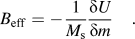 $${B_{{\rm{eff}}}} = - {1 \over {{M_{\rm{s}}}}}{{\delta U} \over {\delta m}}\quad .$$
The energy per unit volume
 $$U = - {M_{\rm{s}}}{\bi{m}} \cdot {{\bi{B}}_{{\rm{ME}}}} + A{\left( {\nabla m} \right)^2} + {K_x}m_x^2 + {K_y}m_y^2 + {K_z}m_z^2\quad ,$$
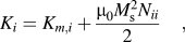
comprehends the Zeeman energy related to the ME field B ME, the exchange energy with a constant A, and the anisotropy terms (K x , K y , K z ), which comprise both material anisotropy (K m,x , K m,y , K m,z ) and shape anisotropy (also known as demagnetization):
 $${K_i} = {K_{m,i}} + {{{\mu _0}M_{\rm{s}}^2{N_{ii}}} \over 2}\quad ,$$
where N ii are components of the demagnetization tensor.
The widely accepted micromagnetic solver, Object-Oriented Micro-Magnetic Framework (OOMMF) Reference Donahue and Porter33 from the National Institute of Standards and Technology (NIST), was used for these simulations. In our case, the ME field enters the equations as a vectorial magnetic field rather than an anisotropy term; therefore, we consider the exchange bias case of switching. The main difference is that in conventional simulations, the magnetic field is extended over the whole devices, whereas the ME field is localized over the part of the FM in contact with the ME material.
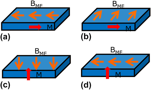
In simulations, we consider several possible geometries for switching, shown in Fig. 3. The magnetization can have an equilibrium direction in-plane, if it is governed by the shape anisotropy. For this case, we set the nanomagnet size to be 40 × 20 × 2 nm. The ME material is in contact with the one side of the largest area. Magnetization is set at M s = 1 MA/m. The ME field can be approximately parallel to magnetization (pointing along the long x-axis of the nanomagnet). We set it at an angle of 160o from the x-axis in-plane. Magnetization reversal occurs when the Zeeman energy overcomes the energy barrier created by shape anisotropy, and we apply the ME field over a time of 100 ps. Alternatively, the ME field can be perpendicular to magnetization in-plane of the nanomagnet. In this case, the magnetization switching happens in a precessional manner (similar to Ref. Reference Nikonov, Bourianoff, Rowlands and Krivorotov34): a short pulse (we use 30 ps in simulations) of ME field causes a deflection of magnetization out-of-plane, and then it continues switching without the field, under the influence of demagnetization.
Geometric schemes of simulated cases of ME switching. (a and b) Magnetization in-plane. (c and d) Magnetization out-of-plane. (a and c) ME field approximately parallel to magnetization. (b and d) ME field approximately perpendicular to magnetization.

The magnetization can also have an equilibrium direction out-of-plane, if material anisotropy exceeds the shape anisotropy and makes this direction more energetically favorable. We take a nanomagnet of the same size as above, 40 × 20 × 2 nm and typical values for such materials M sp = 0.4 MA/m and anisotropy K z =200 kJ M/m3. As before, the ME field can be approximately parallel to magnetization (70° from the plane and the x-axis) or it can be perpendicular to the magnetization, along the x-axis.
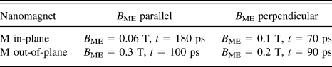
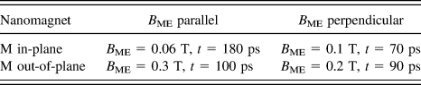
The results of micromagnetic simulations are summarized in Table II in terms of the required values of ME field (which are slightly larger than the critical values) and the corresponding switching delays.
Summary of required ME field and corresponding switching delay for single nanomagnets.
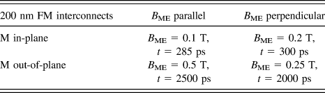
We also simulate switching of FM interconnects. For all directions of magnetization, we take a slab of 200 × 20 × 2 nm size. The ME layer is in contact with one side of the FM wire with the same area as for single magnets. Switching of interconnects occurs first around the ME layer. A domain wall forms between it and the rest of the FM wire. Then, the domain wall propagates toward the other end of the FM wire. Thus, the switching delay of the FM interconnect is mainly determined by the velocity of the domain walls in it. The same angles of the ME field are used here as for single nanomagnets of the same magnetization direction, except the case in Fig. 3(d). For that case, it was found that a different stimulus is needed to create domain walls. We use 2 pulses of ME field, both 80 ps long, one after another: the first ME field pulse along the x-axis and the second ME field pulse at 90° to the x-axis in-plane. The results of micromagnetic simulations for FM interconnects are collected in Table III.
Summary of required ME field and corresponding switching delay for 200 nm long FM interconnects.
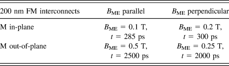
In summary, for both single nanomagnets and FM interconnects, switching of in-plane magnetization is faster and requires smaller ME field. It is in stark contrast with the case of ST switching, where perpendicular magnetization is more favorable, Reference Mangin, Ravelosona, Katine, Carey, Terris and Fullerton35 and leads to smaller critical current and faster switching at a given value of current. Another downside of out-of-plane magnetization is that domain walls tend to reflect from the ends of interconnects. Reference Nikonov, Manipatruni and Young36 That leads to lack of a stable magnetization value at the end of the interconnect. Even for the preferred case of in-plane magnetization, the required ME field is 3–10 times larger than it is currently demonstrated in experiments.
IV. BENCHMARKING RESULTS
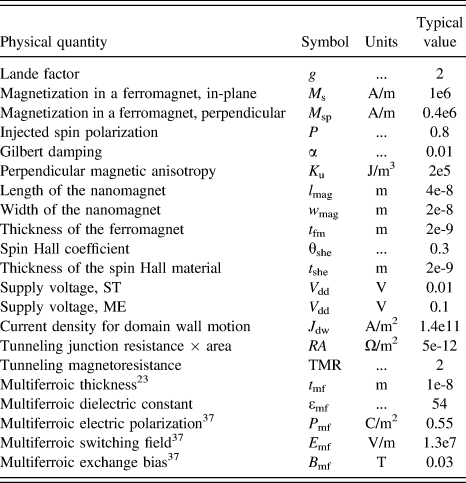
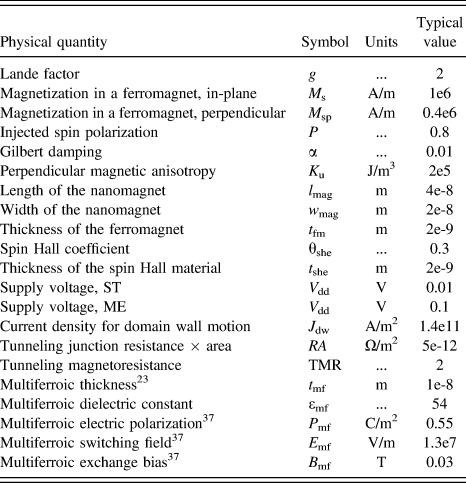
First, we compare various types of switching for spintronic devices. For this, we use the same kind of the device—spin majority gate logic. For the details in the treatment of ST switching please, see Ref. Reference Nikonov and Young7. We have collected the material parameters related to spintronic devices in Table IV. These parameters represent the most recent state-of-the-art experimentally measured values, with the reference where appropriate, or typical values for the corresponding class of materials.
List of material parameters and device used in benchmarking of spintronic beyond-CMOS devices.
For the spin Hall effect switching, we use similar expressions with modified values of the spin polarized current
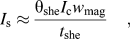 $${I_{\rm{s}}} \approx {{{\theta _{{\rm{she}}}}{I_{\rm{c}}}{w_{{\rm{mag}}}}} \over {{t_{{\rm{she}}}}}}\quad ,$$
where I c is the charge current. For precessional ST switching of an in-plane magnetized nanomagnet (see e.g., Ref. Reference Nikonov, Bourianoff, Rowlands and Krivorotov34), we use the following approximate estimates for the demagnetization field, threshold z-projection of magnetization, charge needed for switching, the gyromagnetic constant, switching delay, and switching energy:
 $${B_{{\rm{dem}}}} = {\mu _0}{M_{\rm{s}}}{m_z}{N_{zz}}\quad ,$$
 $${m_z} = \sqrt {{{\left( {{N_{yy}} - {N_{xx}}} \right)} \mathord{\left/ {\vphantom {{\left( {{N_{yy}} - {N_{xx}}} \right)} {{N_{zz}}}}} \right. \kern-\nulldelimiterspace} {{N_{zz}}}}} \quad ,$$
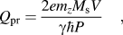 $${Q_{{\rm{pr}}}} = {{2e{m_z}{M_{\rm{s}}}V} \over {\gamma \hbar P}}\quad ,$$
 $$\gamma = {{ge} \over {2{m_e}}}\quad ,$$
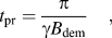 $${t_{{\rm{pr}}}} = {\pi \over {\gamma {B_{{\rm{dem}}}}}}\quad ,$$
 $${E_{{\rm{pr}}}} \approx {Q_{{\rm{pr}}}}{V_{{\rm{dd}}}}\quad ,$$
where V is the volume of the nanomagnet, and N xx , N yy , N zz are diagonal values of the demagnetization tensor calculated according to Ref. Reference Beleggia, De Graef, Millev, Goode and Rowlands38.
For ME switching, as before, we focus on the exchange bias mechanism, which permits a straightforward 180° switching. We use the parameters corresponding to BFO as a ME layer. Reference Heron, Trassin, Ashraf, Gajek, He, Yang, Nikonov, Chu, Salahuddin and Ramesh23 Then, the required electric field, supply voltage, required charge, switching energy, and switching delay are:
 $${E_{{\rm{req}}}} = {{{E_{{\rm{mf}}}}{B_{{\rm{ME}}}}} \mathord{\left/ {\vphantom {{{E_{{\rm{mf}}}}{B_{{\rm{ME}}}}} {{B_{{\rm{mf}}}}}}} \right. \kern-\nulldelimiterspace} {{B_{{\rm{mf}}}}}}\quad ,$$
 $${V_{{\rm{dd}}}} = {E_{{\rm{req}}}}{t_{{\rm{mf}}}}\quad {\rm{,}}$$
 $$Q = A\left( {{P_{{\rm{mf}}}} + {\varepsilon _{{\rm{mf}}}}{\varepsilon _0}{E_{{\rm{mf}}}}} \right)\quad ,$$
 $${E_{{\rm{ME}}}} \approx Q{V_{{\rm{dd}}}}\quad ,$$
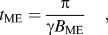 $${t_{{\rm{ME}}}} = {\pi \over {\gamma {B_{{\rm{ME}}}}}}\quad ,$$
where the required ME field is B ME = 0.1 T. Likewise, we can calculate the switching delay per ME cell. We then use methods of Ref. Reference Nikonov and Young7 to estimate those for more complicated circuits.
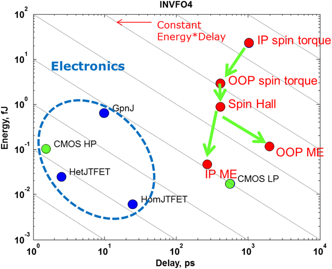
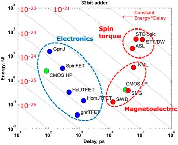
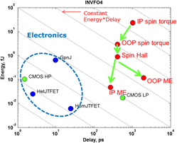
Benchmarking results—switching energy versus switching delay for an inverter with fan-out of 4—are shown in Fig. 4. Both here and further on, we use the following abbreviations for the devices considered: ‘CMOS HP’: high performance CMOS, according to ITRS 39 ; ‘CMOS LP’: low-power CMOS, Reference Avci, Rios, Kuhn and Young40 ‘GpnJ’: graphene pn-junction, ‘HomJTFET’: homojunction tunneling field-effect transistor (FET), ‘HetJTFET’: heterojunction tunneling FET, ‘gnrTFET’: graphene nanoribbon TFET, ‘spinFET’: spin based FET, ‘SWD’: spin wave device, ‘SMG’: spin majority gate, ‘NML’: nanomagnetic logic, ‘ASL’: all spin logic device, ‘STOlogic’: spin transfer oscillator logic, and ‘STT/DW’: spin transfer torque domain wall device. For details on the treatment of each device, please see Ref. Reference Nikonov and Young7.
Switching energy versus switching delay for fan-out of 4 inverters composed of selected devices. Spin majority gates switched by various mechanisms (marked at the red dots) are compared with CMOS transistors (green dots) and electronic beyond-CMOS devices (blue dots). ‘IP’ = in-plane, ‘OOP’ = out-of-plane.
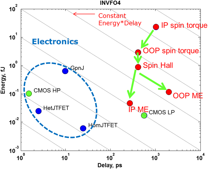
One can notice that the progression of switching technology types from in-plane magnetization ST, to perpendicular magnetization ST and spin Hall effect, to ME switching of in-plane magnetization leads to continually decreasing switching energy. The latter type of technology makes spintronic devices competitive in switching energy with low-power CMOS and tunneling FETs. However, no comparable decrease of switching delay is achieved. The problem of spintronic devices is that their switching speed is still limited by the time it takes for magnetization to rotate by ∼180o angle.
Finally, we turn to a comprehensive picture of spintronic circuits, such as the estimates for a 32-bit ripple-carry adder, shown in Fig. 5. Some spintronic devices can only operate by ST switching, as indicated in the plot. Other devices can operate by ME switching, and they are identified on the plot. We confirm again that ME switched devices achieve lower switching energy. However, their switching speed is still lagging. This observation supports the need for research on ways to achieve faster switching of magnetization.
Switching energy versus switching delay for 32-bit adders composed of selected devices: spintronic (red dots) are compared with CMOS transistors (green dots) and electronic beyond-CMOS devices (blue dots).

V. CONCLUSIONS
We reviewed the results of experiments on ME switching of nanomagnets by oxides adjacent to ferromagnets. We classified mechanisms of switching into magnetostrictive, exchange bias, and surface anisotropy types. The effective ME field has been mapped as a function of the applied electric field. The magnetostrictive mechanism so far has shown the highest ME coefficient. Next, we performed micromagnetic simulations to determine the ME field required for switching a nanomagnet and determined characteristic switching delays for single nanomagnets as well as short-scale spintronic interconnects. Finally, we incorporated these requirements into the framework of benchmarking beyond-CMOS circuits and estimated the performance improvement from the adoption of ME switching on the example of ST majority gates. We conclude that ME switching is crucial for making spintronic logic competitive in terms of switching energy compared with electronic logic. Further research is required to increase the speed of magnetization switching.