
Introduction
Ferrites are a special group of magnetic materials of particular technological interest due to their unique combination of ferromagnetism and large electrical resistance. One of the most important ferrites, nickel ferrite (NiFe2O4), a soft ferrimagnet with high-Curie temperature, relatively large saturation magnetization and high electrical resistivity, was the subject of this research. The combination of desirable properties makes NFO interesting for use in high-frequency[ Reference Cullity and Graham 1 , Reference Spaldin 2 ] and spin filter devices,[ Reference Luders, Barthelemy, Bibes, Bouzehouane, Fusil, Jacquet, Contour, Bobo, Fontcuberta and Fert 3 – Reference Gajek, Bibes, Barthelemy, Bouzehouane, Fusil, Varela, Fontcuberta and Fert 5 ] sensors,[ Reference Zhao, Zhao, Hunter, Suchoski, Gao, Mathews, Wuttig and Takeuchi 6 ] memory,[ Reference Goodenough 7 – Reference Bibes and Barthelemy 11 ] and magnetoelectric composites.[ Reference Li, Wang, Lin and Nan 9 , Reference Shi, Wang, Liu and Nan 10 , Reference Priya, Islam, Dong and Viehland 12 – Reference Nan, Bichurin, Dong, Viehland and Srinivasan 14 ]
Traditionally, magnetic properties have been considered intrinsic and material dependent, so to change a magnetic property significantly, the composition must be altered. Recently, another approach was reported where control over one of the key magnetic properties, coercivity, is possible through proper nanostructuring of the thin film surface.[ Reference Rasic and Schwartz 15 – Reference Rasic and Schwartz 17 ] By patterning the surface with alternating parallel grooves we forced the magnetic domains walls to align along the edges of the features, creating an ‘artificial’ parallel stripe domain structure and reducing the coercivity. All of the initial experimental research, as well as theoretical investigations, supported this explanation of the results. If true, this would allow us to engineer the magnetic properties without changing composition. In combination with traditional methods of altering magnetic properties, such as doping and alloying, this would greatly add to the tunability of magnetic properties. More importantly, it would allow us to select materials based on other criteria (cost, strength, Curie temperature) and then tailor the magnetic properties for optimal performance.
Before we can be certain that these findings are truly due to the surface patterning, however, there remain some unanswered questions. This paper focuses on the prominent questions related to the observed coercivity reduction and providing further insight into the origin of the phenomena.
Experimental
Sample synthesis
The 0.2 molar NiFe2O4 solution was prepared using nickel(II) acetate tetrahydrate (C4H6NiO4·4H2O) and iron(III) nitrate nonahydrate (Fe(NO3)3·9H2O) powders from Sigma-Aldrich. The powders were dissolved separately in a 2-methoxyethanol (CH3OCH2CH2OH) solvent (also from Sigma-Aldrich). The two solutions were then stirred at 70 °C for 2 h before being mixed for an additional 15 min at room temperature.[ Reference Rasic and Schwartz 17 ]
Thin NiFe2O4 films were grown by spin coating the sol-gel solution onto a c-plane (0001) epi-polished sapphire (Al2O3) substrate at 4000 RPM for 30 s. Before film deposition the substrate was cleaned using organic solvents in sequence: methanol, acetone, isopropyl alcohol, followed by heating on a hot plate at 400 °C for 60 s to remove organic contamination and water condensation. The film is then deposited and placed onto a hot plate at 400 °C for 60 s to remove the organic species and create amorphous film. Finally, the film is annealed in a furnace at 750 °C for 15 min to crystallize the film. The process can be repeated several times to create thicker films. This substrate, solution molarity and processing parameters were previously shown to give biaxially textured NFO thin film.[ Reference Seifikar, Calandro, Deeb, Sachet, Yang, Maria, Bassiri-Gharb and Schwartz 18 ]
Nanoimprint lithography (NIL) was used to create surface nanostructures on the thin films. The method consisted of creating a polydimethylsiloxane (PDMS) stamp with the desired pattern and then transferring that pattern onto the surface of NFO thin films. After the initial spin coating of the NFO thin film the PDMS stamp was pressed directly onto the spin coated NFO thin film with immediate pyrolysis at 400 °C for 60 s. The stamp was then removed and the patterned amorphous NFO film placed in the furnace for 15 min at 750 °C to crystallize the film, as described previously. For thicker samples, two planar layers are spin coated, pyrolyzed and crystallized on a wafer first, with only the last (third) layer being patterned using NIL.
For patterning, a PDMS stamp of a commercially available compact disc (CD) was used similar to previous reports.[ Reference Rasic and Schwartz 15 – Reference Rasic and Schwartz 17 ] The feature size of a CD is approximately 750 nm with a 1500 nm period. To access the features of the CD, the top aluminum layer was removed and the patterned polycarbonate plastic was cleaned and used for patterning. To prepare the PDMS stamp, a Sylgard-184 Silicone Elastomer Kit from Dow Corning was used. The silicone base and curing agent were mixed in a 10:1 weight ratio for several minutes before being placed in the desiccator until there were no noticeable gas bubbles in the liquid. The liquid was then poured over the pattern master and placed in the desiccator until all gas bubbles were removed to ensure the liquid penetrates completely into the features of the master and no gas bubbles remain trapped inside. The master with the liquid is then cured in an oven for 24 h at 70 °C. Such long curing time ensures large molecules in the liquid have sufficient time to fully crosslink,[ Reference Efimenko, Wallace and Genzer 19 ] ensuring the stamp retains its chemical and mechanical integrity during imprinting.
Characterization of NiFe2O4 thin films
A Rigaku Smartlab x-ray diffractometer was used to evaluate the texture and the phases present in the films. θ − 2θ x-ray diffraction (XRD) scans were performed from 15° to 60° using a Cu K α radiation source with wavelength of λ = 1.5418 Å. The scans were done at room temperature with step size of 0.04° and dwell time of 2 s. The peaks were identified using Bragg's law and correlated with the reference PDF file (JCPDS File No. 003-0875).
The sample topography was studied using atomic force microscopy (AFM) in tapping mode on a Cypher AFM (Asylum Research). The images were taken with 512 lines at scan rate of 1 Hz. The scan angle of 90° was used for best image quality.
A JEOL 2010F transmission electron microscope (TEM) was used for cross-sectional analysis of the surface features and to investigate the NFO film microstructures. The electron source of the JEOL 2010F uses ZrO/W (100) Schottky type field emission gun and achieves 0.19 nm point resolution. The microscope was operated with an accelerating voltage of 200 kV. A FEI Quanta three-dimensional (3D) FEG focused ion beam (FIB) was used to prepare the NFO samples for TEM imaging. To prevent charging of the highly resistive NFO film and sapphire substrate during imaging, the samples were carbon coated before starting the ion milling. The samples were prepared using 30 kV accelerating voltage for both electron and ion beams. For best viewing, standard mode was used, with a 0.14 nA electron beam current and 10 pA ion beam current. The initial cut was made with a 15 nA ion current, which was reduced gradually to 50 pA for polishing. In addition, elemental maps were collected using energy dispersive spectrometry (EDS) on an aberration corrected scanning TEM (FEI Titan 80–300) to evaluate the chemical composition of the film and investigate the phase purity.
Finally, the magnetic hysteresis was measured in a superconducting quantum interference device (SQUID) with a vibrating sample magnetometer (VSM) from Quantum design. The measurements were conducted with the surface of the NFO thin films parallel to the magnetic field (‘in-plane’). Samples were measured at room temperature with magnetic field up to ±7 Tesla. Peak VSM amplitude of 5 mm with 2 s averaging time was used to improve measurement precision, especially around zero magnetization. Before measuring, the magnet was oscillated from 7 to 0 T to minimize flux pining. To reduce the background noise, the samples were mounted on a special quartz sample holder supplied by Quantum Design. GE7031 varnish (Lake Shore Cryotronics) was used to attach the samples to the sample holder.
Results and discussion
Single layer NFO thin films were fabricated using a similar procedure as described here. The details of the procedure used as well as the results of measurements can be found in the original paper.[ Reference Rasic and Schwartz 15 ] AFM microscopy revealed good patterned transfer from the PDMS stamp to the samples with no noticeable defects.[ Reference Rasic and Schwartz 15 ] This result was further confirmed with TEM and XRD measurements.[ Reference Rasic and Schwartz 15 ] XRD measurements revealed the films to be single phase inverse spinel nickel ferrite with no impurities and no noticeable difference between the surface patterned films and planar ones.[ Reference Rasic and Schwartz 15 ] Also, both films showed preferential orientation in the <111> direction corresponding to reports in previous work.[ Reference Seifikar, Calandro, Deeb, Sachet, Yang, Maria, Bassiri-Gharb and Schwartz 18 ] Before we can eliminate compositional changes as the source of the coercivity reduction, however, more evidence is needed.
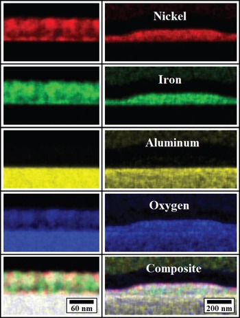
EDS maps of nickel, iron, aluminum and oxygen were collected for both planar and patterned samples and are shown in Fig. 1. The planar film is shown on the left side while the patterned film is shown on the right side of Fig. 1. A composite image is also shown for comparison. Figure 1 shows a clear and sharp interface between the film and substrate for the nickel and iron atoms indicating no diffusion into the substrate. More importantly, aluminum is found only in the substrate indicating there is no diffusion from the substrate to the films. Finally, oxygen is found in both the film and the substrate as expected. Precise spatial separation between the film and the substrate indicates the film to be pure single phase and sapphire to be a good substrate for producing high quality NiFe2O4 films, as it does not interact with the film. This result provides a more conclusive evidence to support hypothesis that the origin of the coercivity reduction is the surface topography as concluded previously.[ Reference Rasic and Schwartz 15 – Reference Rasic and Schwartz 17 ]
Elemental maps of planar (left) and patterned (right) NFO thin film. Elemental nickel (red), iron (green), aluminum (yellow), oxygen (blue) as well as the composite image are shown separately.

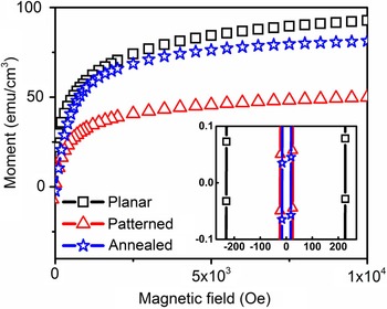
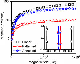
While the magnetic measurements revealed an impressive 89% reduction of coercivity in surface patterned NFO thin films, they also showed a 44% reduction in the saturation magnetization.[ Reference Rasic and Schwartz 15 ] Since the AFM, TEM, and XRD showed no evidence of reduced crystallinity, the reduction in saturation magnetization was attributed to larger porosity of the patterned NFO thin films.[ Reference Rasic and Schwartz 15 ] To further evaluate these claims, the same patterned NFO thin film was annealed for additional 5 min at 750 °C, followed by 10 min anneal at 850 °C. This should provide enough thermal budget to be able to evaluate if coercivity reduction reported previously[ Reference Rasic and Schwartz 15 ] is due to the reduction of crystallinity in the patterned film and/or larger sample porosity. AFM scans revealed the topography of the sample to be unchanged by the process of additional annealing. Magnetic measurements on the additionally annealed sample (‘Annealed’) are shown in Fig. 2. For comparison, the magnetic measurement results on the planar and surface patterned NFO thin films originally reported[ Reference Rasic and Schwartz 15 ] are also shown.
Magnetization hysteresis of additionally annealed NFO thin film. Previously reported results[ Reference Rasic and Schwartz 16 ] for planar and patterned films are shown for comparison. Inset shows a higher magnification image centered at the origin.

Looking at the magnetic hysteresis curves in Fig. 2 we see that the saturation magnetization of patterned sample approaches that of the planar sample with the additional annealing. This indicates that there indeed was larger porosity in the patterned films and/or that they were not fully crystallized even if this was not observed with any other characterization method. This discrepancy between the optimal processing parameters for the planar and patterned samples could be explained by greater film thickness in the hills of the surface patterned films making them require larger thermal budget.
Unfortunately, reduced crystallinity could also cause a reduction in coercivity. The higher magnification image shown in the Fig. 2 inset, however, shows no increase in the coercivity of the additionally annealed pattern film. This confirms that the coercivity reduction is indeed a physical phenomenon resulting from the surface patterning and not a product of insufficient film crystallization. The small differences in the coercivity values can be explained by small variations in the film, pattern and flux pinning of the SQUID magnet; these differences are negligible as compared with planar films value. Moreover, the coercivity of a thin film is expected to increase with increased annealing, contrary to what is seen. This serves as further confirmation that the coercivity reduction seen in the patterned samples is not related to any material or processing specific property.
To further study the coercivity reduction thicker NFO samples were made.[ Reference Rasic and Schwartz 16 , Reference Rasic and Schwartz 17 ] AFM scans confirmed that the surface patterns were again transferred without any defects[ Reference Rasic and Schwartz 16 , Reference Rasic and Schwartz 17 ] with the lower limit on the pattern period estimated at 500 nm.[ Reference Rasic and Schwartz 16 , Reference Rasic and Schwartz 17 ] XRD, TEM, and SQUID measurements revealed that fabricating thicker films one layer at a time resulted in improved texture and crystallinity as compared with bulk annealing.[ Reference Rasic and Schwartz 16 ] In addition, the layer-by-layer grown films showed the same preferential orientation in the <111> direction and similar texture, hence this fabrication method was chosen.[ Reference Rasic and Schwartz 16 ] Furthermore, all surface patterned NFO thin films showed a reduction in coercivity regardless of the feature size.[ Reference Rasic and Schwartz 17 ] This indicates that the observed coercivity reduction is a consequence of the imprinting process itself.
To determine if this was the case, a sample was partially imprinted with a flat PDMS stamp (‘Imprinted’) and compared with the part of the sample that was not imprinted (‘Planar’). Magnetization measurements, shown in Fig. 3, reveal both the planar and imprinted samples have similar values of saturation magnetization and show similar magnetization curves. In addition, both samples have saturation magnetization values similar to those reported previously.[ Reference Rasic and Schwartz 16 ]
Magnetization hysteresis of NFO thin films imprinted with a flat PDMS stamp. Inset shows higher magnification image centered at the origin.

A higher magnification image of the magnetization data, shown in inset of Fig. 3, reveals both samples to have similar coercivities, indicating that the process of imprinting does not affect the magnetic properties of the thin films by itself. Furthermore, the values obtained are comparable with the results obtained for the planar film reported previously[ Reference Rasic and Schwartz 16 ] indicating good consistency in the results. Thus we conclude that the observed coercivity reduction is not a result of the imprinting process.
Finally, the effect of different feature orientation with respect to the magnetic field for in-plane measurements was studied. It is well known that magnetic wires have different hysteresis loops depending on how they are oriented relative to the magnetic field.[ Reference Sattler 20 , Reference Goolaup, Singh and Adeyeye 21 ] Due to the shape of the surface pattern of our films, it could be imagined as a series of parallel nanowires grown on a surface of thin films. As such one might expect them to have different magnetic response depending on their orientation relative to the magnetic field.
The magnetization measurements, seen in Fig. 4, were done ‘in-plane’ with the sample surface feature orientated parallel and perpendicular to the magnetic field. Magnetization measurements show both sample orientations have similar magnetic response with the value of saturation magnetization for the features oriented perpendicular to the magnetic field being slightly larger. This result, while surprising at first, is in accordance with what is reported for the magnetic wires of similar diameter as the surface features of our samples.[ Reference Van Thiem, Tu and Phan 22 ] More importantly, we conclude that this effect is small and that there is no significant influence of the feature orientation to the field direction on the saturation magnetization of our samples.
Magnetization hysteresis of a surface-patterned NFO thin film measured with the features parallel and perpendicular to the magnetic field. Inset shows a higher magnification image centered on the origin.

Looking at the values of coercivity in inset of Fig. 4, we again observe a similar response for both feature orientations with respect to the magnetic field, in accordance to what has been reported for wires of similar diameter.[ Reference Van Thiem, Tu and Phan 22 ] This indicates that the orientation of the features is not a significant contributor to the coercivity, contrary to what is often observed in the case of isolated high aspect ratio structures such as wires and rods.
This could be explained by the fact that here the surface features are fairly large and that, contrary to wires and rods, the features are not isolated but are connected to the surface of a thin film underneath. In other words the ‘wires’ are part of the film, thus, the total magnetic response comes not only from the features, but from the sample as a whole, where the features are only on the surface. While the features might behave similarly to the wires, in that they have a preferred magnetic orientation along the long axis, the magnetic domains created in the features do not extend completely into the film underneath. The net magnetic response is then a combination of the magnetic properties of surface features and the planar film underneath, with the planar film dominating the saturation, but the feature geometry driving the magnetic domain structure and thus the coercivity.
Conclusions
A recently reported method of reducing coercivity in thin films by surface patterning could be technologically very useful. Before it can be fully implemented though, better understanding of the phenomena is needed. In this work, EDS measurements confirmed the absence of chemical interdiffusion between the film and the substrate and thus eliminated chemical changes as a possible origin of reduced coercivity. Furthermore, we have shown that with additional heating of the patterned films it is possible to achieve saturation magnetization similar to that of the unpatterned films with no effects on coercivity. Another possible alternative, that the source of the effect is coming from the process of imprinting itself, was tested using a flat stamp. The results demonstrated that the imprinting process does not in itself change the magnetic properties of the material. Finally, to gain greater understanding of the origin coercivity reduction, measurements with different orientation of surface features relative to the magnetic field were made. The results were in accordance with what would be expected for magnetic wires of similar diameter. However, the effect is small in contrast to what is usually observed in magnetic wires. This shows us that the features cannot be looked at individually, but the sample has to be considered as a whole with one side flat and the other one patterned. One possible explanation is that the final magnetic hysteresis is a combination of the contribution from the surface features and the flat film underneath. In which case the underlying continuous nickel ferrite film dominates the saturation magnetization behavior and the patterning of the surface layer controls the magnetic domain structures and thus the coercivity.
Acknowledgments
This work is supported by the NSF (HRD-0833184), NASA (NNX09AV07A) and NSF- PREM (1523617) awards. The authors acknowledge the use of the Analytical Instrumentation Facility (AIF) at North Carolina State University, which is supported by the State of North Carolina and the National Science Foundation.