I. INTRODUCTION
Electronically steerable antenna arrays are very attractive for mobility scenarios in future broadband satellite communication systems [Reference Stark1]. Poor aerodynamic properties and mechanical complexity are the main disadvantages of mechanically steerable antennas on mobile platforms. In contrast, low–profile antennas are well suited for compact antenna arrays. Patch radiators are commonly used, here. The calibration of these antenna elements is an important task regarding the overall antenna performance, such as gain, side lobe level, and/or pointing accuracy [Reference Porat and Friedlander2]. An autonomous calibration system with online monitoring capability and simple calibration procedure is desirable. The monitoring solution should be adaptable to any array size.
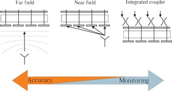
Generally, one can distinguish between two calibration concepts – the external and the internal one (an overview is given in Fig. 1). The former one is the best–known approach and yields the most accurate results with plane wave excitation at bore sight, since, in general, this reproduces the normal operation condition of an array [Reference Nuteson, Stocker, Clarck IV, Haque and Mitchell3]. However, for obvious reasons, this concept may not always be practical for mobile users, at least in the transmit case. Indeed, as calibration parameters may vary in time due to environmental effects, a necessary recalibration becomes difficult with the far-field method. The near-field calibration concept relies on reference antennas placed in close vicinity of the array, which is more convenient for mobile users. However, the calibration accuracy suffers from the phase-error sensitivity and the complexity of the underlying calibration models. In addition, applicability of near–field approaches to arbitrarily large arrays is not evident.
Overview of main calibration approaches with different ways to inject a reference signal.

A calibration method with integrated networks is ideally suited to on-line monitoring purposes. According to [Reference Nuteson, Stocker, Clarck IV, Haque and Mitchell3] the internal calibration for a receiving antenna is normally carried out by injecting a calibration signal behind each antenna element. Commonly, this is achieved by means of a coupler, as it has been demonstrated in the patch antenna array design in [Reference Passmann, Villino and Wixforth4]. In that way, only the hardware behind the coupler is calibrated. Since this approach does not take the mutual coupling of radiating elements and finite array effects into account, the calibration accuracy is limited compared to the far–field approach [Reference Nuteson, Stocker, Clarck IV, Haque and Mitchell3].
The in-situ probes proposed in this contribution combine advantages of both calibration approaches – the monitoring possibility of the internal probes and the calibration accuracy of the far-field method. These probes are placed inside the cavity of a patch antenna. The fundamental patch mode is excited by the probes, thus approximating the far-field situation. This allows for amplitude and phase-error detection of both the radiating elements and the connected (active) circuitry. Following the ideas introduced in [Reference Stark, Johannsen and Jacob5], this paper provides a more general overview of the calibration concepts – in addition to the magnetically coupled a capacitively coupled probe design is presented. Furthermore, the sensitivity of the probes to the effects of inevitable fabrication tolerances is addressed. In order to demonstrate the applicability of the probes, the calibration coefficients of array configurations are analyzed.
This contribution is organized as follows: In Section II, both a capacitively and a magnetically coupled in-situ probe are investigated. They are critically assessed and the integration in a multilayer antenna is presented. A sensitivity analysisis performed and experimental verification at K-band is provided. The calibration accuracy is discussed next in Section III. Finally, the application of the calibration scheme to different array configurations is shown.
II. CALIBRATION PROBES
A) Approach
The in-situ probes to be proposed in this work should have the ability to detect mutual coupling and finite array effects. For this purpose, the fundamental patch mode has to be excited by the probes since this corresponds to the actual antenna operation.Ideally, no additional information for the calibration is needed.
Since the approach has to be applicable both for receive and transmit antennas, the matching of the probes is another important requirement. For instance, the calibration network of the receiving antenna studied in this work has an active transmit path for which strong reflections have to be avoided.
Since the calibration probes are to be placed inside the patch cavity, effort has to be spent to mask the calibration network itself to the antenna array as much as possible under normal operation conditions. That is, the probes should not disturb the radiation purity of the fundamental patch mode.
1) Capacitively coupled probe
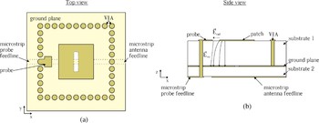
First, a capacitively coupled in-situ probe design is presented. The simulation arrangement with its cross–sectional view is depicted in Fig. 2. A small patch-like probe fed through a vertical interconnection access (VIA) is placed on the top layer. The fringing E-fields of the fundamental patch mode are utilized to couple the calibration signal from the probe to its feed line. The calibration signal strength can be adjusted by varying the distance between the patch and the probe and/or byadjusting the size of the latter. However, due to the asymmetry of the arrangement, the radiation pattern is degraded. As a direct consequence the far–field beam is tilted.
Top (left) and cross-sectional (right) view of the capacitively coupled in-situ probe design operating at 20 GHz.

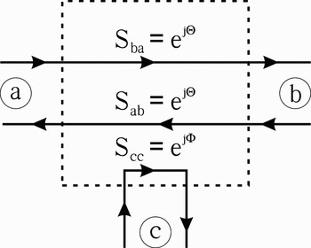
In addition, matching is a problem of the design. One can describe the complete structure as a three-port network. It is well known that a lossless and reciprocal three-port network cannot be matched at all ports simultaneously [Reference Pozar6]. Figure 3 clarifies this in the present context. The antenna feed port is denoted as (a), the antenna patch, i.e. the radiating port, as (b), and the probe as (c). That is, a lossless one-port probe in combination with the perfectly matched patch antenna (two-port network) cannot be matched at all.
A three-port network representation of a single-feed (capacitively coupled) probe in combination with a patch antenna.

2) Magnetically coupled probe
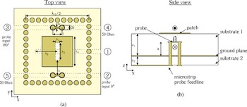
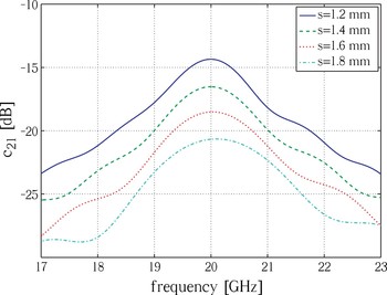
The matching problem described in the previous section can be avoided by utilizing a two-port probe, with one port being terminated by 50 Ω. To this end, a magnetically coupled loop is proposed and investigated. The corresponding schematic of the proposed probes integrated inside the cavity of the patch is shown in Fig. 4. The resulting four-port device can be described as a coupler, in which the magnetic coupling can be adjusted by changing the distance s between the coupled line of the probe and the slot of the antenna feed line. Due to limitations of the fabrication process the loop height a cannot be varied here. Figure 5 shows the frequency response of the coupling strength c 21 (power flow from the probe to the feed line of the patch) for various values of s. This dependence can be used for adjusting a predefined signal level, for instance, to comply with power limitations of the calibration circuitry. In normal patch-operation mode the coupling c 21 defines additional signal loss – a result of the reciprocal network.
Schematic of the magnetically coupled in-situ probes operating at 20 GHz. Parameter values: s = 1.50 mm, s 1 = 0.45 mm, s 2 = 2.30 mm, s 3 = 2.32 mm, s 4 = 3.30 mm, l = 1.00 mm, w = 0.15 mm, r = 0.30 mm, λ0 = 15.00 mm, a = 0.30 mm, a 1 = 0.50 mm, and a 2 = 0.20 mm.

Variation of coupling strength c 21 as function of frequency.

To maintain radiation symmetry two probes have to be arranged in parallel. The electrical length of the coupler amounts to 180°. This can be explained by the description of the radiating element as a piece of transmission line having an electric length of 180° [Reference Pozar6]. Thus, the two probes have to be excited with opposite phase (ports 2 and 3 in Fig. 4). The relation between the port excitation of the probes and the radiation symmetry is demonstrated in Fig. 6. Four relevant combinations are examined. Port numbers are defined as in Fig. 4. Ports 2 and 3 appear as the proper choice. This is verified by the far-field radiation results. Only with an opposite phase excitation of the two parallel probes a symmetrical radiation can be obtained. As a result, the desired fundamental patch mode radiates notably. The observed deviation in directivity compared to the reference case is attributed to the broader beam width which, in turn, is a result of inevitable fringing fields. Nevertheless, the obtained radiation emulates the patch behavior in the normal operation mode when excited by the microstrip feed. Hence, mutual coupling and finite array effects are essentially taken into account.
Radiation pattern of the patch excited by different port combinations as a function of elevation angle Θ in (a) the x-z-plane (E-plane) and (b) the y-z-plane (H-plane).

B) Multilayer design at 20 GHz
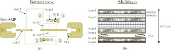
The calibration scheme is tested in a 20 GHz receiving array in the context of the SANTANA project [Reference Holzwarth7]. The schematic of the in-situ probes from Fig. 4 has been provided with an additional balun, as shown in Fig. 7. A Marchand balun [Reference Marchand8] is employed to excite the probe ports with opposite phase and equal amplitude as required for a symmetric radiation pattern. In order to maintain the matching condition of the probes, the unused ports have to be terminated by 50 Ω resistances. RF-resistors in a 0302 SMD package from IMS [9] are used in this contribution. For measurement purposes Mini-SMP connectors are mounted on the back side.
Schematic of the in-situ probes with integrated Marchand balun (left) and the corresponding multilayer stack (right). Parameter values of the patch and probe are referred in Fig. 4

The circuit in Fig. 7 provides radiation symmetry and good matching but is not scalable. This is because the test structure occupies more area than available in antenna arrays with one half free–space wavelength element spacing. In a full-scale antenna the balun structure presented here is to be integrated in additional layers beneath the antenna which is not a problem in standard industrial processes. However, with our in-house fabrication process this is only feasible with reduced accuracy. Therefore, as a proof of concept, a demonstrator with as few layers as possible is considered. As a consequence the multilayer stack is realized as two separated units being bonded with an anisotropic conductive adhesive (ACA) as indicated in Fig. 7. Otherwise a substrate layer thickness of 50 µm is required to fabricate the proposed design within standard multilayer processes.
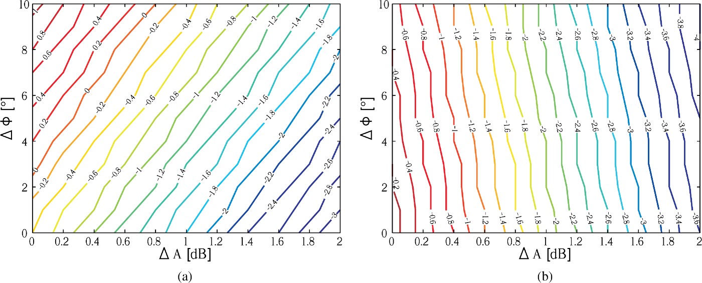
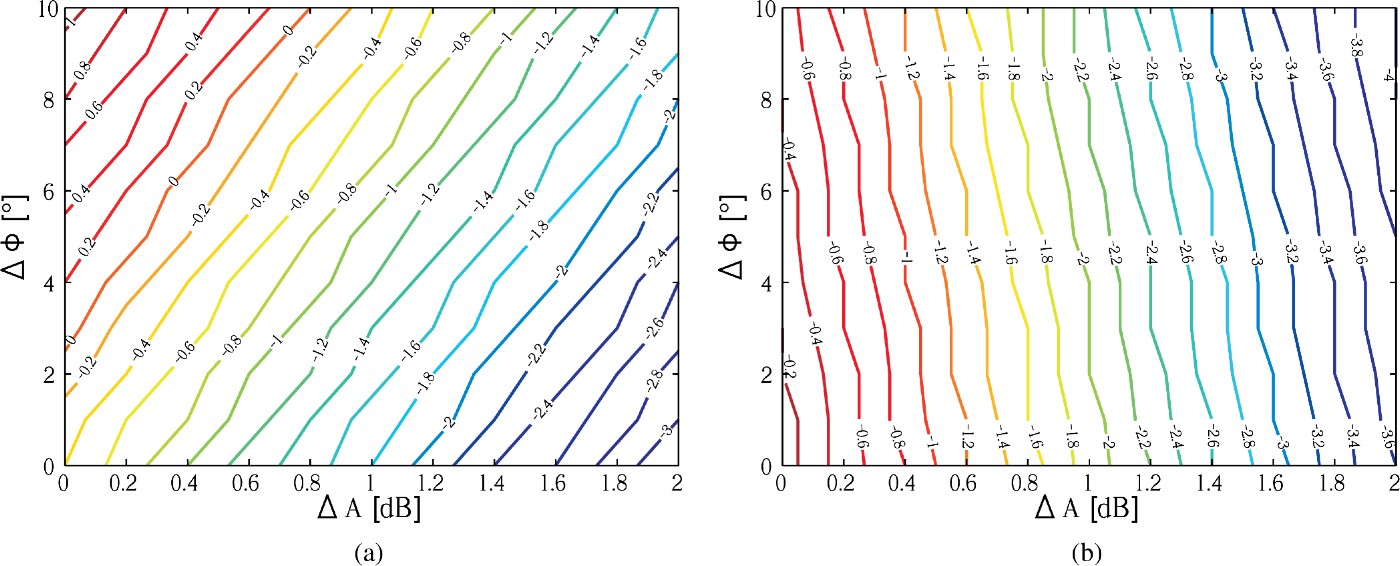
So far, the complex excitation of the probes was considered to be ideal. By including a feeding structure like a balun, the probes' sensitivity against inevitable amplitude and phase uncertainties becomes an issue. Thus, a quantitative assessment particularly of the pattern degradation is mandatory. We performed such a tolerance analysis by means of simulation. For this purpose the probes are excited by different combinations of amplitude ΔA and phase errors ΔΦ. The resulting beam pointing error is shown in Fig. 8 (0.1° simulation accuracy). As demonstrated in Fig. 8 the deviation is relatively small for ΔA and ΔΦ values up to 0.4 dB and 5°, respectively. In the H-plane the pointing error is almost independent from the phase error ΔΦ. The remaining misalignment of 0.4° in the E-plane for nominal excitation results from the slightly asymmetric (and unavoidable) feeding port arrangement in the simulation setup. However, the same misalignment is observed in the reference case.
Probes sensitivity analysis based on amplitude and phase tolerances of the Marchand balun. Pointing error of the far field beam as function of tolerances in (a) E- and (b) H-plane.
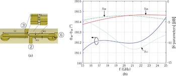
To obtain reasonable coupling values the balun is realized in a broadside manner. This simplifies the quantitative coupler design. The arrangement of the Marchand balun along with the design parameters is shown in Fig. 9(a). The signal at port six is equally distributed between ports two and three, exciting the probes with opposite phase and equal amplitude. Within a relative bandwidth of more than 2.5 % the simulation of the Marchand balun with CST (Computer Simulation Technology) Microwave Studio [10] shows a matching better than 11 dB, and phase and amplitude imbalance of 0.2° and 0.05 dB, respectively (see Fig. 9(b)). The obtained phase imbalance is equalized by the feeding lines on layer 4 that have slightly different electrical length. As a result, the assumed symmetrical probe excitation is only affected by the amplitude imbalance of 0.05 dB. This amplitude error is negligibly small, as demonstrated in Fig. 8.
(a) Enlarged schematic of the integrated Marchand balun. Parameter values: R = 0.3 mm, L 1 = 0.08 mm, L 2 = 1.7 mm, w 1 = 0.07 mm, w 2 = 0.28 mm, w 3 = 0.25 mm. (b) Simulation results of the Marchand balun.

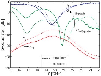
The multilayer design of a single radiation element with the in-situ probes and the integrated balun has been realized and measured. Matching of the antenna and the probes as well as the coupling c 21 are shown in Fig. 10. For comparison the simulation results are also included. The effect of the Mini-SMP connectors is eliminated by a TRL (Through Reflect Line) calibration. Thus, comparison between simulation and measurement is conducted at the same reference plane. Satisfactory agreement between the simulation and measurement results can be stated. The behavior of the measured coupling c 21 is similar to the simulated one. The simulated matching condition of the patch that represents an important parameter is reproduced in practice. A negligibly small shift of the resonance frequency is observed. It can be attributed to fabrication tolerances.
Measured (solid lines) and simulated (dashed lines) S-parameters of the antenna element from Fig. 7.

III. ARRAY CALIBRATION
A) Receive scenario
A straightforward calibration approach is considered. The array is subjected to a linearly polarized plane wave at normal incidence. This is compared to the probe excitation. All probes are simultaneously excited with equal amplitude and proper phase to emulate the plane wave scenario. In both cases, the distribution of the element output signals is recorded, one element being chosen as reference. The amplitude and phase deviations from this reference are taken as the respective calibration coefficients. A close match is expected.
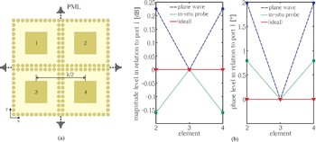
Different array configurations are investigated to demonstrate the potential of the proposed in-situ calibration probes. First, a 2 × 2 array is considered and analyzed by means of a CST simulation. The antenna elements are numbered as depicted in Fig. 11(a). To account for finite array effects the antennas are subjected to open-space boundary conditions. The perfectly matched layers (PML) are located at a predefined distance to the array.
(a) Arrangement of the investigated 2 × 2 antenna array with integrated in-situ probes (coordinate system as in Fig. 4). (b) Detected amplitude and phase deviations of the 2 × 2 array (antenna one is the reference element).

The resulting amplitude and phase deviations of the antenna elements at 20 GHz are shown in Fig. 11(b). The amplitudes and phase angles of antennas 2–4 are related to antenna 1, taken as reference element in the array. In this way, variations of the received signal levels caused by differences in the excitations are compensated. The amplitudes and phase angles of the calibration scheme using (ideal) couplers placed outside the antenna cavity are included in Fig. 11(b) as well. As such, a coupler does not excite the patch itself as the antenna imperfections are not taken into account. Therefore, the amplitudes and phases of all patches are equal, here.
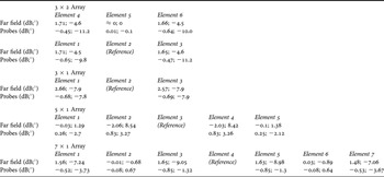
Table 1 contains the amplitude and phase deviations of a 3 × 2, 3 × 1, 5 × 1, and 7 × 1 antenna arrays, obtained in the same manner as described before. The table layout reproduces the element arrangement in the xy-plane of the array. The reference element is indicated. For the 3 × 1 array amplitude and phase errors for plane wave and probe excitation are almost equal whereas in the case of the 3 × 2 array the phase deviation doubles for the in-situ probes. This coincides with the results obtained for the 2 × 2 array. Simulation results of the 5 × 1 and the 7 × 1 array demonstrate that, essentially, the amplitude and phase deviations do not depend on array size.
Simulated amplitude and phase deviations of a 3 × 2, 3 × 1, 5 × 1, and 7 × 1 antenna array excited by a far field source (E-plane) as well as the integrated in-situ probes in comparison to a reference element.

Despite small residual errors the relative phases of the elements excited by the plane wave are reproduced by the excitation through the in-situ probes. The relative magnitudes resulting from plane wave and probe excitation exhibit an inverse slope with small difference in absolute values. Nevertheless, all investigated antenna arrays show the same inverse magnitude response. This suggests that this effect could be used as a general calibration rule. The calibration approach does not include coupling caused by the feeding networks. Simulation indicates that this coupling effect is small enough to be neglected without a significant degradation of calibration accuracy.
B) Transmit Scenario
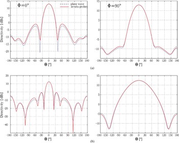
Figure 12(a) represents the far field of the 3 × 2 array operated in the transmit mode. The signals are applied to the regular feed ports. The levels are individually corrected according to the respective deviations obtained from the far field and the probes calibration, respectively (listed in Table 1). In case of calibration with the in-situ probes the available far-field results are not considered. Despite a small increase in the side lobe levels the agreement between the plane wave and the in-situ calibration is good, meaning that the far–field pattern emulated by the probes is not only valid for a single radiator. Similar investigations are conducted for the 5 × 1 array. The far–field results, depicted in Fig. 12(b), again show a close match for the two calibration schemes, thus demonstrating the validity of the proposed approach for larger arrays.
Far-field radiation pattern of (a) the 3 × 2 and (b) the 5 × 1 array with compensated amplitude and phase excitation estimated from Table 1.

C) Discussion
The precisely reproduced behavior of the antenna elements' phases and magnitudes indicates the potential of the in-situ probes. The observed coincidence between plane wave and probe excitation demonstrates the ability of the probes to emulate mutual coupling and finite array effects. No additional information for the calibration procedure is required, resulting in well–suited calibration approach for the intended on-line monitoring scenario.
In digital beamforming systems more advanced calibration procedures are applicable, which allow one to determine and correct the inter-element coupling [Reference Kuhlmann, Jalas and Jacob11]. Their implementation, however, is beyond the scope of this contribution and is the subject of ongoing research.
IV. CONCLUSIONS
In-situ calibration probes are presented in this work. These probes are integrated in the cavity of a patch antenna. They allow for the detection of errors caused by finite array effects and mutual coupling. In combination with the detection possibility of active circuitry a very accurate calibration is achievable in theory. Measurement results of a single–antenna element equipped with the probes are in agreement with simulation. The potential of the in-situ probes is demonstrated by means of simulation of antenna arrays with different arrangements and sizes operating at K-band. It is shown that there is good agreement between the far field and the probe calibration – a feature making the probes applicable for online monitoring tasks.
ACKNOWLEDGEMENTS
The authors wish to acknowledge the funding of this work by the German Aerospace Center (DLR) on behalf of the German Federal Ministry of Economics and Technology (BMWi) under research contract 50YB0709.
 Alexander Stark received the Dipl.-Ing. degree in electrical engineering from the Technische Universität Hamburg-Harburg (TUHH), Hamburg, Germany, in 2006. Since 2006, he has been with the Institut für Hochfrequenztechnik, Technische Universität Hamburg-Harburg, Hamburg, Germany. His research interests include the design and packaging of highly integrated active antenna arrays up to millimeter-wave frequencies. He was the recipient of the EuMC Young Engineers Prize at the 40th European Microwave Conference in 2010.
 Benjamin Rohrdantz received the Dipl.-Ing. degree in electrical engineering from the Technische Universität Hamburg-Harburg, Hamburg, Germany, in 2009. Since 2009, he has been with the Institut für Hochfrequenztechnik, Technische Universität Hamburg-Harburg, Hamburg, Germany. His research interests include system analysis and design of active microwave antenna arrays.
 Ulf Johannsen received the Dipl.-Ing. (M.Sc.) degree in electrical engineering from the Technische Universität Hamburg-Harburg, Hamburg, Germany, in 2009. Since 2009, he has been a Ph.D. student with the Eindhoven University of Technology (TU/e), the Netherlands. His research interests include Antenna-on-Chip (AoC), Antenna-Array-on-Chip (AAoC), integrated mm-wave antennas, and mm-wave antenna measurement.
 Arne F. Jacob was born in Braunschweig, Germany, in 1954. He received the Dipl.-Ing. and the Dr.-Ing. from the Technische Universität at Braunschweig in 1979 and 1986, respectively. From February 1986 to January 1988 he was a Fellow at CERN, the European Laboratory for Particle Physics in Geneva, Switzerland. From February 1988 to September 1990, he was with the Accelerator and Fusion Research Division of the Lawrence Berkeley Laboratory, University of California at Berkeley, USA. He then joined the Institut für Hochfrequenztechnik, Technische Universität Braunschweig as a Professor. Since October 2004, he has been a Professor at the Institut für Hochfrequenztechnik, Technische Universität Hamburg-Harburg, Germany. His current research interests include the design, packaging, and application of integrated (sub-)systems up to millimeter frequencies, and the characterization of complex materials. Arne Jacob is a Fellow of the IEEE, a member of the VDE-ITG, the EuMA, and the URSI Commission B.