Introduction
As more and more devices today use wireless connections, the demand for fast and reliable communication has grown quickly. The rapid evolution of modern communication systems, including the expansion of wireless networks, the infrastructures of internet of things, and defense-related technologies, has driven the demand for reconfigurable frequency selective surface (FSS) designs [Reference Munk1 –Reference Li and Shen3]. By integrating active components such as varactor diodes, positive-intrinsic-negative (PIN) diodes, or other tunable elements, it becomes possible to dynamically modify the frequency response, bandwidth, and even the polarization characteristics of the FSS [Reference Bakshi, Mitra and Teixeira4 –Reference Wen, Wang, Hong, Pan and Zheng8]. This adaptability is particularly essential in environments where operating conditions depend on the dynamic availability of the electromagnetic spectrum for the intended applications, interference conditions, or the environment-based specific limitations.
While significant progress has been made in the development of reconfigurable FSSs for microwave and millimeter-wave bands, comparatively fewer studies have addressed the low-frequency band implementations. At lower frequencies, unit-cell dimensions tend to increase, presenting challenges for compactness, integration, and angular stability [Reference Naseri, Pourmohammadi, Fei, Melouki, Iqbal and Denidni9, Reference Bora, Pardhasaradhi and Madhav10]. Moreover, low-frequency FSS applications such as for the L/S band communication systems, low-frequency radar, and shielding effectiveness often require wide frequency tuning ranges without compromising the transmission characteristics in the intended band, which becomes a challenge to achieve [Reference Alhaj Hasan, Nguyen, Kuksenko and Gazizov11 –Reference Ali13].
The AFSS structures are made of self-repeating periodic elements with properties that allow them to control the transmission or reflection of electromagnetic (EM) waves. The selection of an element design determines the behavior and performance of FSS filters, which can also control the radiating behavior of the antennas when used as a superstrate. When PIN or the varactor diodes are embodied in this FSS superstrate, AFSS can electronically switch the antenna beam to make the structure suitable for the beam steering applications without the need for any external phase shifters. Switching ON and OFF the PIN diodes integrated FSS has been used to change the radiation pattern of the antennas to cover the entire azimuth plane [Reference Elzwawi, Kesavan, Alwahishi and Denidni14 –Reference Kong, Li, Luo and Gao17]. However, by employing some innovative methods, the number of required elements can be drastically reduced, and ultimately, the design complexity of the beam-switching antenna can be reduced [Reference Phon, Ghosh and Lim18].
Varactor-based active frequency selective surfaces (AFSS) are an innovative concept that can also solve many problems in the beam-switching of antennas. This type of reconfigurable FSS uses the inherent advantages of varactor diodes, tunable semiconductor devices that allow real-time adaptability and precise frequency control [Reference Borhani-Kakhki and Denidni19, Reference Ahmed, Singh and Esselle20]. Integration of the varactor diodes in the FSS structure provides a revolutionary way to dynamically control the EM wave impinging on it, making it an essential technology for future-generation communication systems [Reference Carreira21]. The main idea behind using the varactor-based active FSS is its capability to continuously switch between the reflective and transmissive states through electronic capacitance adjustment in the diodes integrated within the surface. Coupled with varactor diodes, the frequency response of an AFSS can be tuned to help antennas to reconfigure their beam positions [Reference Ebrahimi, Shen, Withayachumnankul, Al-Sarawi and Abbott22 –Reference Sathuluri and Sasikala24].
The varactor diode-based AFSS provides numerous advantages that make it better suited to overcome the beam-switching problems. It achieves compactness as it integrates varactor diodes in the FSS structure, thus removing the bulkier external components and setting it up for streamlined implementations even in space-constrained applications [Reference Isa, Jusoh, Sabapathy, Nebhen, MR, MN, QH, HA and MN25 –Reference Beneck, Das, Mackertich-Sengerdy, Chaky, Wu, Soltani and Werner27]. This integration also supports low power consumption since it requires minimal power for operation and thus makes it suitable for energy-consumption-based communication systems [Reference Alwareth, Ibrahim, Zakaria, Al-Gburi, Ahmed and Nasser28, Reference Gong, Lu, DT, Niyato, Shu, DI and YC29]. A compensation mechanism based on a reconfigurable FSS with angular stability to compensate for the deviation introduced by the varactor diode is proposed in [Reference Anand and Mittal30]. The PIN diode-operated dual-polarized tunable FSS working in the LTE-D band is reported in [Reference Bai, Yan, Li, Wang, Zheng, Wang and Qu31]. A tunable FSS with wide reconfigurability between 1.51 and 3.84 GHz, which has been achieved using varactor and PIN diodes simultaneously, is reported in [Reference Yang, Li, Cao and Wang32]. Although the structure exhibits angular stability up to 70°, it is a single polarization structure, which may find limited applications. To realize high transmittance, a varactor-tunable FSS based on the equivalent circuit model (ECM) is proposed in [Reference Zhang, Ding and Bozzi33]. Further, in the case of varactors, the frequency tuning is done with high precision because of high sensitivity and tunability. This results in greater adaptability of the AFSS under varying operating conditions, which makes it suitable for the beam steering applications. These benefits bring powerful capabilities to varactor-based active FSS reconfigurable antennas, which motivates researchers to implement innovative methods in designing and fabrication of this type of AFSS.
This paper advances reconfigurable FSS technologies by introducing a simple varactor-based AFSS design operating in the electromagnetic spectrum’s L, S, and ISM bands. The key contributions include the development of optimized AFSS design principles and integrating varactor diodes for precise real-time frequency tuning, which may be used for dynamic beam-switching without the need for external phase-shifting components to reduce structural complexity. The paper comprehensively analyzes reconfigurable FSS for TE/TM modes with angular stability. The equivalent circuit (EC) model has been developed to demonstrate the congruence of the theoretical and structural responses. The paper addresses the challenges in designing the reconfigurable FSS. It thus proposes a simple reconfigurable FSS that can be tuned in the 1.53–3.1 GHz communication band with a high tuning ratio.
The paper is organized as follows. Section “Proposed AFSS unit-cell” presents the proposed AFSS unit-cell design. In Section “Equivalent circuit model”, the EC model of the reconfigurable AFSS, which shows tunability, is developed. Section “Theoretical validation” presents theoretical validation. Section “Fabrication and experimental results” presents the fabricated and experimental results. In Section “State-of-the-art comparison”, the state-of-the-art comparison is made. Finally, Section “Conclusion” concludes the work.
Proposed AFSS unit-cell
The geometric structure of the unit-cell of the proposed AFSS is shown in Fig. 1(a) and (b). The unit-cell consists of two metallic surfaces placed at opposite faces of a dielectric. The upper metallic surface has a double square loop with stubs, while the bottom layer is a single square loop with stubs. These square loops in the unit-cell are responsible for the bandpass behavior of the AFSS. The RT-Duroid 5880 (εr = 2.2, tanδ = 0.0008) with a thickness (h) = 1.6 mm has been used as the substrate material. The capacitive gap between two square loops on the upper layer is connected through a varactor diode to obtain the frequency tuning. The proposed structure’s upper layer has an outer square loop of 18.80 and 1.40 mm, while the inner square loop has an 8.00 mm length and 1.20 mm width, respectively. The structure’s bottom layer comprises a single square loop 8.00 mm in length and 1.20 mm in width with stubs.
Proposed AFSS unit-cell (a) front, (b) back view, and (c) 3D view.

The bottom layer is used for the biasing arrangement. It is connected to the upper layer by four metallic vias of radius (R 1) = 0.5 mm to bias the varactor diode. The biasing arrangement uses the unit-cell’s geometry and the lumped elements to bias the varactor diode. For this purpose, four inductances are used at the bottom layer to complete the DC biasing arrangement. The biasing arrangement enables the varactor diode to be reverse-biased when the DC voltage is applied to the structure. The design parameters of the unit-cell are given in Table 1. A simple design structure with a high tuning ratio has been developed. The 3D view of the structure of the unit-cell under the full wave simulation environment in the CST microwave studio is shown in Fig. 1(c).
Design parameters of unit-cell

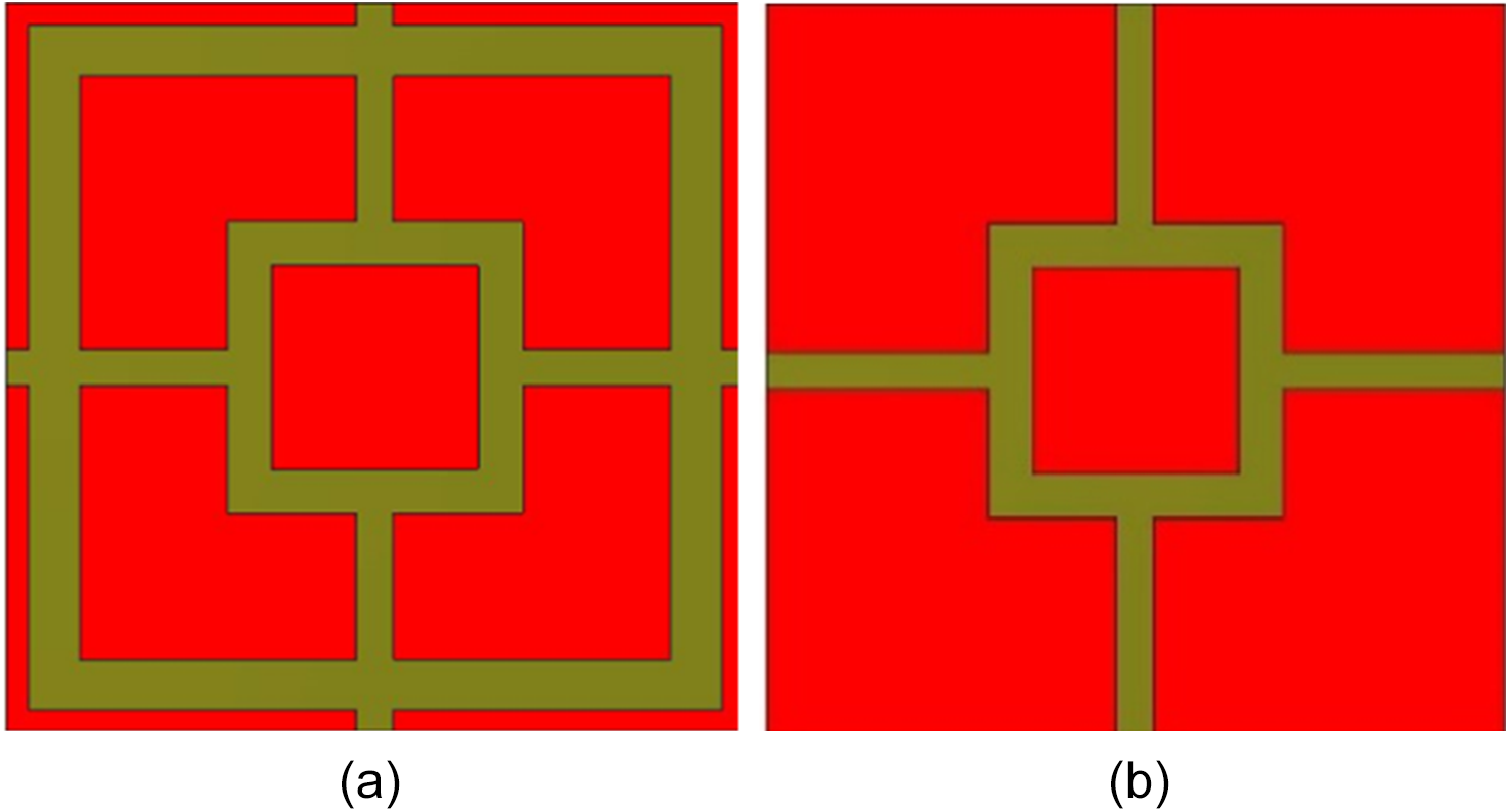
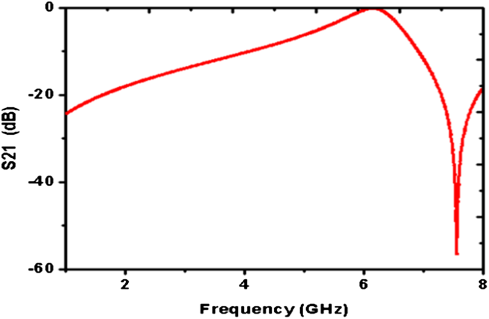
Inherently, the square-loop has band-stop filtering characteristics. However, two concentric square loops in the unit-cell connected through the varactor diode result in the reconfigurable bandpass AFSS design. The unit-cell has a periodicity (P) of 20 mm. To start the design, a simple square-loop structure without tuning elements, as shown in Fig. 2, was simulated in the CST Microwave Studio. The response of the structure is shown in Fig. 3.
Proposed unit-cell (a) front and (b) back view.

Response of the structure of Figure 2(a) and (b).

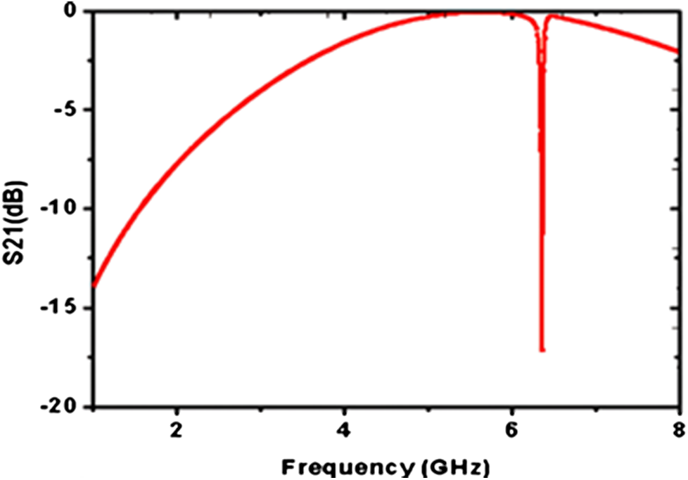
The structure exhibits a bandstop behavior in the 1–4 GHz band, where S21 is less than – 10 dB. Further, the transmission pole and zero appear at 6 and 7.5 GHz, respectively. It indicates that inherently, the topology has bandstop characteristics in the 1–4 GHz band. To make the structure reconfigurable and to accommodate active and biasing elements, slots have been cut in the stubs at the top and bottom layers, as shown in the structure. Further, as indicated in Fig. 4(a) and (b), four vias of R 1 = 0.5 mm are placed to provide the biasing voltage to the active element at the top layer. The response of these arrangements is shown in Fig. 5. From this figure, it is interpreted that the transmission pole shifts marginally from 6 to 5.5 GHz, but the transmission zero shifts significantly from 7.5 to 6.30 GHz.
Unit-cell with vias (a) front, and (b) back view.

Response of the structure of Figure 4(a) and (b).

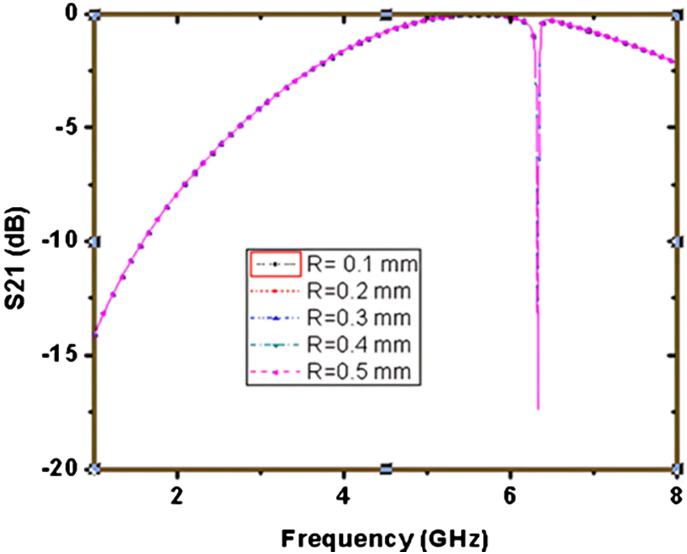
In this scenario, the −3 dB bandstop response is 3.4 GHz. The effect of the change of radius of the metallic via’s and the slot position has been parametrically varied, but no significant change has been observed. Figure 6 shows the structure’s response when the radius of the vias is varied from 0.1 to 0.5 mm. In the structure, as shown for biasing the active elements, four inductors per unit-cell have been placed at the bottom layer in Fig. 2(b). The purpose of the inductor is only to pass the direct current without interfering with the RF signal. The value of the inductor is to be selected so that it does not change the unit-cell response.
Response of the structure by varying the radius of the via’s.

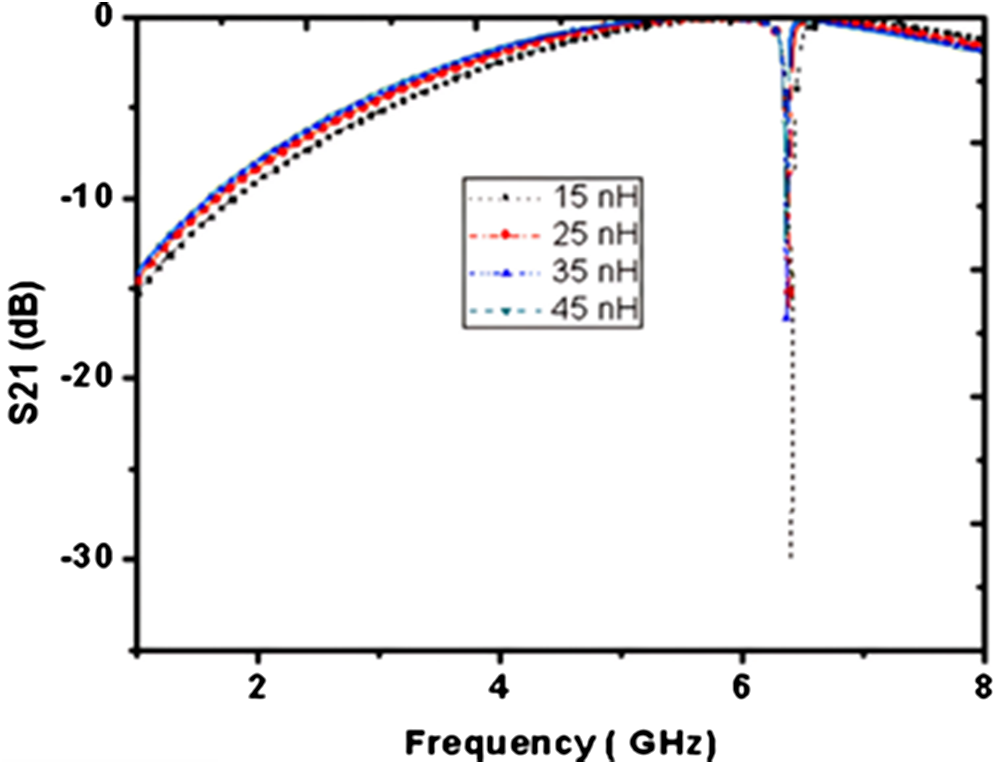
An inductor of 15 nH each has been placed in the slots at the bottom layer to meet this requirement. It has been noticed that it does not influence the unit-cell response, as shown in Fig. 5. The structure has been simulated with different values of inductors. There is no significant change in the response, as shown in Fig. 7.
Response of the structure of varying inductors.

To achieve the reconfigurability in the L–S bands of the electromagnetic spectrum, the varactor diode SMV1430, represented by the series combination of resistance (RR1), inductance (LL1), and capacitance (CC1), where RR1 = 3.15 ohms, LL1 = 0.45 nH, and CC1 = 1.24 pF, is used in the structure. A total of 4 varactor diodes per unit-cell have been placed on the top layer, as shown in Fig. 2(a). When the diode is placed in the circuit, in the OFF state, the response is like the response to the previous case observed with the inductor. Further, to demonstrate that the structure exhibits a similar response to that of the unit-cell without a varactor diode. Finally, with the varactor diode, the structure is simulated. Its response is shown in Fig. 8. The result shows the proposed structure’s frequency tuning capability when the varactor diode’s capacitance (CC1) varies from 1.24 to 0.31 pF, corresponding to 0 and 30 V, respectively.
Response of the structure of varying capacitance.

These are the two extremes of the applied biasing voltages to this diode. For the three intermittent values of CC1, the unit-cell’s response is also shown in Fig. 8. It is observed that the structure can be reconfigured from 1.53 to 3.1 GHz with a tuning bandwidth of 101.30%. The minimum −3 dB bandwidth of the 100 MHz band is achieved at the lowest operating band, corresponding to CC = 1.24 pF, and 800 MHz bandwidth, corresponding to CC1 = 0.31 pF.
Equivalent circuit model
For the physical insight into the working mechanism, the EC model is derived from the interpretation of the surface current density (J S) on the unit cell. The J S for different cases is shown in Fig. 9(a)–(c).
Surface current densities of the structure (a) without diode at 1.58 GHz, (b) with diode at 1.58 GHz, and (c) with diode at 3.1 GHz.

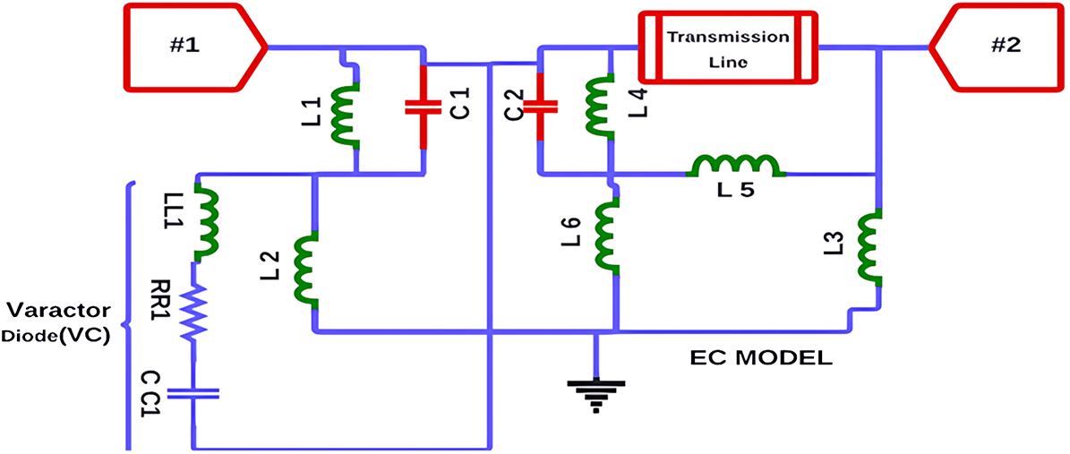
In Fig. 9(a), the inter unit-cell gap shows a discontinuity in the J s, thus having a capacitive (C 1) effect. The interconnecting stubs between unit cells have a stronger surface current, which indicates its inductive behavior. Thus, this inductor (L 1), in parallel to the gap capacitance (C 1), forms a parallel L–C circuit in the EC model, as shown in Fig. 10. The symmetric outer loop is modeled as an inductor (L 2). The inner square loop is modeled as (L 6). The inner square loop, along with the stub, represents another resonating circuit where inductance and capacitance have been modeled as L 2 and C 4, respectively. The back side of the structure has a square loop dominated by its inductive behavior, which is modeled by L 3 in Fig. 10. The metallic vias used to connect the upper and lower layers of the metallic strips also show the inductive behavior modeled by L 5.
EC model of the structure.

To make the structure tunable, a varactor diode can be placed to connect the outer square loop to the inner square loop, which is modeled as a series RLC circuit represented by the combination of RR1, LL1, and CC1. The value of CC1 can be set to different values. In the case of 1.24 pF (0 V biasing voltage), the current density on the unit-cell surface is shown in Fig. 9(b). In this case, the stronger J S on the outer loop can be observed but diminishes at the inner loop’s corners, indicating the current flow through the diode and thus controlling the resonance frequency [Reference Guo, Zheng, Chen, Ding, Sang, Yuan, Guo and Fu34]. When CC1 is reduced to 0.31 pF, the J S is further reduced, as shown in Fig. 9(c). In this case, due to the lower value of the CC1, the quality factor is reduced, and the bandwidth is increased, compared to the case when CC1 = 1.24 pF.
The ECM of the unit cell can be drawn using the inductors and capacitors. The lumped elements are characterized using the band of operation and the parasitic and other effects for the full-wave EM Simulations. The value of inductors can be calculated using the approximate design equation in which L, W, t, and kg are the length of the metallic segment, the width of the segment (in µm), the thickness of the segment, and the correction factor, respectively [Reference Ganie, Jha and Sharma35]. Here, m is an integer that represents the inductance number, as shown in Fig. 10. The correction factor is due to the use of the dielectric support on which the inductor has been formed. The value of the correction factor is 0.59 to include the effect of the ground plane:
 \begin{align}{L_m}(\text{\textit{n}H}) &= 2 \times {10^{( - 4)}} \times l \left[\text{ln}{\kern 1pt} \;\left(\frac{l}{{W + t}}\right) + 1.193 \right. \nonumber\\
&\quad \left.+ 0.2235\;\left(\frac{{W + t}}{l}\right)\right] \times \text{kg}.\end{align}
The capacitance value between the sections in the EC model is a closed expression without dielectric material and is calculated using (2), where again, m is an integer representing the capacitance number in the EC model, as shown in Fig. 10 [Reference Hong and Lancaster36]. In this case, L,  ${\varepsilon _0},{\varepsilon '_r}$Furthermore, gK is the length of the segment (in µm), the relative permittivity of free space, the real part of the relative permittivity of the substrate material used, and the inter-element gap distance, respectively:
 \begin{equation}{C_m}\left( {{p\text{F}}} \right) = \left( {2L{\varepsilon _0}/\pi } \right){\sin ^{ - 1}}(\pi {g_k}/2L).\end{equation}
However, when the dielectric material is considered, the capacitance relation gets modified as follows [Reference Hong and Lancaster36]:
 \begin{equation}{C_d}\left( {{p\text{F}}} \right) = \left( {2l{\varepsilon _0}{{\varepsilon '}_r}/\pi } \right){\sin ^{ - 1}}(\pi {g_k}/2l).\end{equation}
Based on these equations, the lumped parameters of the EC model have been retrieved and shown in Table 2. The two-port networks play a critical role in modeling RF and microwave systems, where frequency-dependent behavior and impedance matching are key design considerations.
Design parameters of the unit-cell

Thus, here, the objective is to derive the ABCD parameters that comprehensively describe the electrical characteristics of the circuit, especially its resonance and high-frequency performance.
The analyzed network comprises interconnected reactive components and a transmission line, forming a two-port symmetric structure. Here, the model comprises the following network element combinations:
i. Parallel LC Circuit (
 ${L_1}$ (Inductor) and
${C_1}$ (Capacitor) at Port 1.
ii. Series Inductor (
${L_2}$) grounded, influencing impedance.iii. Varactor diode (
$R{R_1},L{L_1}$,
$C{C_1}$) providing tunable resonance.iv. Parallel LC circuit
${L_4}$ (inductor) and
${C_2}$ (capacitor). Connected via a transmission line.v. Delta network (
${L_3}$
${L_5}$
${L_6}$) at Port 2, where


•
${L_6}$ and
${L_3}$ are grounded.•
${L_5}$
${L_6}$ are connected to
${L_4}$ ||
${C_2}$.•
${L_3}$
${L_5}$ are connected to Port 2.


Outer loop: A parallel combination of ${L_1}$ (inductor) and
 ${C_1}$ (capacitor). Inner loop: A more complex structure comprising a parallel combination of
 ${C_2}$ (capacitor) and
 ${L_4}$ (inductor), delta configuration of three inductors:
 ${L_3}$, and .
Transmission line: Connecting the inner loop to the backside loop.
The admittance of the parallel combination of  ${L_1}$ and
 ${C_1}$ with the impedance of a series inductor
 ${L_2}$ Impedance of varactor diode
 $CC1$ (for a case CC1 and parallel circuit and
 ${C_2}$) are calculated as =
 ${\text{j}\omega }{C_1}$+
 $ = {\text{j}\omega }{L_2},{Z_{{\text{CC}}}}$=
 $R{R_1}$+
 $L{L_1}$+
 $1{\text{j}\omega }CC{_1},{Y_{{\text{D}}}}$ =
 ${\text{j}\omega }{C_2}$+
 $1/j\omega L{_{4}}$.
The delta configuration is converted into a Y (star) configuration with admittances.
 ${Y_{{L_3}}}$,
 ${Y_{{L_5}}}\& $
 ${Y_{{L_6}}},{Y_{{L_3}}} = \frac{{{L_3}{L_6}}}{{{L_3} + {L_5} + {L_6}}}$,
 ${Y_{{L_5}}} = \frac{{{L_3}{L_5}}}{{{L_3} + {L_5} + {L_6}}}{Y_{{L_6}}} = \frac{{{L_5}{L_6}}}{{{L_3} + {L_5} + {L_6}}}$, respectively.
The ABCD parameters are calculated as
 \begin{equation}ABC{D_A} = \,\left[ {\begin{array}{*{20}{c}}
1&0 \\
{{Y_{\text{A}}}}&1
\end{array}} \right],\end{equation}
 \begin{equation}ABC{D_B} = \,\left[ {\begin{array}{*{20}{c}}
1&{{Z_{\text{B}}}} \\
{0}&1
\end{array}} \right],\end{equation}
 \begin{equation}ABC{D_{{\text{CC}}}} = \,\left[ {\begin{array}{*{20}{c}}
1&{{Z_{{\text{CC}}}}} \\
{0}&1
\end{array}} \right],\end{equation}
 \begin{equation}ABC{D_D} = \,\left[ {\begin{array}{*{20}{c}}
1&0 \\
{{Y_{\text{D}}}}&1
\end{array}} \right],\end{equation}
 \begin{equation}ABC{D_{{Y_{L6}}}} = \left[ {\begin{array}{*{20}{c}}
1&{j\omega {Y_{{L_6}}}} \\
{0}&1
\end{array}} \right],\end{equation}
 \begin{equation}
ABC{D_{{Y_{{L_3}}}}} = \,\left[ \begin{array}{*{20}{c}}
1& { j\omega {Y_{{L_3}}}} \\
{0}&1
\end{array} \right],\end{equation}
 \begin{equation}ABC{D_{{Y_{{L_5}}}}} = \,\left[ {\begin{array}{*{20}{c}}
1&0 \\
{\frac{1}{{j\omega {Y_{{L_5}}}}}}&1
\end{array}} \right].\end{equation}
The cascaded ABCD matrix for the network is $ABC{D_{Total}}$:
 \begin{align}ABC{D_{Total}} &= ABC{D_A} \times ABC{D_B} \times ABC{D_{{\text{CC}}}} \times ABC{D_D} \nonumber\\
&\quad \times ABC{D_{{Y_{{L_6}}}}} \times ABC{D_{{Y_{{L_3}}}}} \times ABC{D_{{Y_{{L_5}}}}}\end{align}
This results in the calculation of the ABCD parameters, which are as follows:
 \begin{equation}A = 1 + j\omega {Y_{{L_6}}}{Y_{{\text{D}}}} + j\omega {Y_{{L_3}}}{Y_{{\text{D}}}},\end{equation}
 \begin{equation}B = j\omega {Y_{{L_3}}} + j\omega {Y_{{L_5}}} + j\omega {Y_{{L_6}}} + {Z_{{\text{CC}}}}\end{equation}
 \begin{equation}C = {Y_{{\text{A}}}} + {Y_{{\text{B}}}} + {Y_{{\text{D }}}} + \frac{1}{{j\omega {Y_{{L_5}}}}}\end{equation}
 \begin{equation}D = 1 + j\omega {Y_{{\text{D}}}}{Y_{{L_5}}}.\end{equation}
Thus, using the conversion formula from ABCD to S-parameters, we can deduce the  ${S_{11}},{S_{22}},{S_{21}},{S_{12}}$. The circuit exhibits reciprocity, ensuring that the transmission properties of the circuit are correct.
Theoretical validation
To validate the concept and accuracy of the retrieved lumped parameters of the unit cell as shown in Table 2, the reconfigurable response of the unit cell is shown in Fig. 11. The comparison of the result of the unit-cell simulation in the CST Microwave Studio and the analytically obtained value of the responses are shown here for the different values of the varactor capacitances. The analytical and simulated results agree to reveal the accuracy of the EC model of a tunable FSS, which has seldom been investigated in the literature.
Comparison of unit cell and EC model responses.

It is clear from the simulation results that the proposed AFSS and the EC model can reconfigure the frequency between 1.53 and 3.1 GHz band for different values of the varactor diode’s capacitance range of 1.24 to 0.31 pF. These capacitances correspond to the two extremes, i.e., 0 and 30 V, which are applied biasing voltages to the SMV1430 [Reference Jha, Mishra and Sharma37].
Fabrication and experimental results
The AFSS was fabricated using the traditional wet etching of the planar circuit board (PCB), and the pattern was created using screen printing on both sides of the copper-cladded Rogers RT5880 substrate material. Once the PCB was fabricated, vias were manually drilled and connected via metallic wires with a radius of 0.5 mm. The AFSS structure of 10 × 10 unit-cells (20 cm × 20 cm) was prototyped as shown in Fig. 12. The biasing arrangement of the AFSS structure is shown in Fig. 13(a)–(c). The front view of the AFSS structure in which it is shown that all the outer square loops are interconnected to each other, on which the positive terminal of the supply voltage is connected. Thus, at any given point, the supply voltage is made available to all the outer loops of the unit-cells. Since the cathode of all the varactor diodes is connected to the outer loop, the positive supply voltage is made available to the cathode of all the varactor diodes in each unit-cell of the AFSS structure. It is evident from Fig. 13(a) that all the diodes in a unit cell are connected in parallel. Thus, this simple biasing technique activates all the diodes in a unit cell.
Fabricated structure front and back, with experimental setup.

Biasing arrangement (a) front face, (b) back face, and (c) schematic diagram.

The biasing arrangement of the back side of the AFSS structure is shown in Fig. 13(b). In this figure, all the backside square loops are connected through the inductors placed in each stub. It is pertinent that the size of the bottom square loop is the same as the size of the inner square loop at the front face of the unit-cell. These loops are connected through the four no’s of metallic vias per unit-cell. The negative supply is made available through the arrangement at the inner loop of the front face of the AFSS. The schematic diagram of the interconnect of the via is shown in Fig. 13(c). Since the anode of the varactor diode is connected to the inner loop. Thus, the negative supply is available for the varactor diode. Therefore, a reverse biasing potential is available across each varactor diode for reconfiguration.
The response of the structure was measured in the Antenna and Microwave Design Laboratory, Shri Mata Vaishno Devi University, India, using a bistatic measurement setup, as shown in Fig. 12(c). The experimental arrangement comprised two pairs of horn antennas operating between 1–2 and 2–4 GHz, respectively. Furthermore, considering the antennas’ maximum dimension (M), the far-field distance of these antennas at their maximum operating frequency is calculated using the formula  ${\text{2 \times }}{M^{\text{2}}}{{/\lambda }}$. The maximum aperture width of the horn antenna used in the measurement was M = 23.5 cm, and thus, for the far-field criteria measurement, the horn was placed at a distance of 1.5 m away from the AFSS. The power supply voltage was varied from 0 to 30 V, and the responses of the structure for the various angles of incidence are shown in Figs. 14 –17.
Simulated and measured response for AOI = 0o (a) TE, (b) TM mode.

Simulated and measured response for AOI = 15o (a) TE and (b) TM mode.

Simulated and measured response for AOI = 30o (a) TE and (b) TM mode.

Simulated and measured response for AOI = 45o (a) TE and (b) TM mode.

Measurement at normal incidence
The structure was measured for the normal and angular incidence of the incident wave on it. The measurement was done by first measuring the transmission coefficient in the free Space (S 21) (without structure) for reference, and then, the transmission coefficient of the prototype was measured. The response of the structure for the normal incidence of the electromagnetic (EM) wave in the transverse electric (TE) and transverse magnetic (TM) modes is shown in Fig. 14(a) and (b), respectively. In the TE mode, the FSS has a 1.58–3.0 GHz simulated and 1.53–3.1 GHz measured tunable frequency range. Similarly, from Fig. 14(b), it is revealed that the simulated and the measured tuning ranges for TM mode are 1.57–3.0 and 1.56–2.70 GHz, respectively. For the TE mode, the simulated and measured frequency tuning range is in good agreement. However, the maximum operating frequency for the TM mode has been reduced to 2.70 GHz. This is mainly due to the tolerances associated with the fabrication process, the effect of handheld soldering in the laboratory, and the characteristic variation of the individual varactor diode. The tuning ratio is defined as the fou/fol, where fou and fol are the resonant frequencies of the upper and lower tuned bands, as shown in Table 3.
Comparison of angular performances

Angular incidence
In addition to the normal incidence, the structure has also been tested for the angular incidences of 15⁰, 30⁰, and 45⁰. The responses of the structure for the AOI = 15⁰, AOI = 30⁰, and AOI = 45⁰ for TE and TM modes are in Figs. 15, 16, and 17, respectively.
It is evident from these figures that with the increase in the angle of incidence, the insertion loss increases and the operating band shrinks. This is mainly due to the fabrication tolerance and the change in the characteristic impedance of TE and TM modes with a change in the angle of incidence. It is expected that by enhancing the fabrication facility, fabrication tolerances can be minimized.
However, with conciseness, we have demonstrated the dual-polarized response of the reconfigurable FSS structure up to the 45⁰ angle of incidence. For the comparison, the other performance indices of the proposed tunable FSS are placed in Table 3.
State-of-the-art comparison
To ascertain the contribution of the proposed reconfigurable FSS, it has been compared to the existing structures, and the state-of-the-art comparison is shown in Table 4. This table shows that the proposed FSS has a wider tuning ratio than others, except for the structure presented in [Reference Bai, Yan, Li, Wang, Zheng, Wang and Qu31]. However, it is at the cost of circuit complexity as varactor and PIN diodes have been used simultaneously in [Reference Bai, Yan, Li, Wang, Zheng, Wang and Qu31]. In addition, the structure proposed in [Reference Bai, Yan, Li, Wang, Zheng, Wang and Qu31] is polarization-sensitive, limiting its applications. Most of the dual-polarized structures have been measured for angular insensitivity up to 45° except the structure reported in [Reference Carreira21]. However, that structure uses double dielectric layers, resulting in a high insertion loss. In view of this comparison, it is concluded that the proposed structure in this manuscript offers a high tuning ratio, with reasonably low insertion loss and polarization insensitivity up to 45°. The structure may find its applications in stealth technology and beam steering of the antennas for the ISM and sub-6 GHz band applications.
State-of-the-art comparison of reconfigurable FSS

a On state of PIN diode.
Conclusion
This paper proposes a simple dual-polarized AFSS with angular stability up to 45º. Using varactor diodes, it has been demonstrated that the AFSS can be reconfigured over the 1.53–3.10 GHz frequency band, offering a high tuning ratio of 2.02. The proposed unit-cell has been rigorously analyzed to retrieve the network parameters of the EC Model for different reconfigurable states. Due to the dual-polarized reconfigurable response, in addition to the conventional use in the radome and the stealth technology, newser applications may be found in the beam steering of the antennas. Since the structure has stable angular responses, it may also be used in tilted-beam-steered antenna design in the future.
Author contributions
Ashish Suri conceptualized and interpreted the findings of the various papers and wrote the manuscript draft. Kumud R. Jha supervised, reviewed, and helped arrive at the manuscript’s conclusion.
Funding statement
This research received no specific grant from any funding agency, commercial or not-for-profit sectors.
Competing interests
The authors report no conflict of interest.

Ashish Suri (MS, IEEE, M-ISTE, M-IE) received the Bachelor’s degree in Electronics Engineering from the University of Pune, Maharashtra, India, in 2001; the Master’s degree in Electronics and Communication Engineering from Punjab Technical University, India, in 2011; and is currently pursuing PhD degree in Electronics and Communication Engineering from Shri Mata Vaishno Devi University, Katra, UT of J&K, India. In 2001, he joined Model Institute of Engineering & Technology as a Lecturer and was promoted to Assistant Professor in 2007. In 2008, he joined Shri Mata Vaishno Devi University as an Assistant Professor. His current research includes microwave active component design for future wireless applications.

Kumud Ranjan Jha (IEEE M’17–SM’18, FIE (I)) received the Bachelor’s degree in Electronics and Communication Engineering from The Institution of Engineers (India), Kolkata, India, in 1999; the Master’s degree in Electronics and Communication Engineering from the Birla Institute of Technology, Ranchi, India, in 2007; and the PhD degree in Electronics and Communication Engineering from the Jaypee University of Information Technology, Waknaghat, India, in 2012. From September 2013 to September 2014, he was a Postdoctoral Fellow with the Department of Electrical and Computer Engineering at San Diego State University, San Diego, CA, USA. Before joining academia, he also served in the Indian Air Force for over one and a half decades. In 2007, he joined Shri Mata Vaishno Devi University, Katra, India, as an Assistant Professor and has been a Full Professor since 2020. He is the co-inventor of an Indian patent (published). He has authored/co-authored more than 90 research articles in journals and conferences. He has also co-authored the book Terahertz Planar Antennas for Next Generation Communication. He is credited with the book chapters in Multifunctional Antennas and Arrays for Wireless Communication Systems (IEEE Press/Wiley, USA, 2021). His current research interests include microwave/RF passive/active component design and terahertz electronics for future wireless applications. Dr. Jha is the recipient of the 2012 Raman Fellowship Award from the University Grant Commission, Government of India, for postdoctoral study in the USA. He is a Fellow of the Institution of Engineers (India). Dr. Jha is also a recipient of International Travel Grants from the Govt. of India to participate in IEEE Antenna Propagation Society Symposiums.