Introduction
Photovoltaic (PV) materials development is entangled with major technological achievements in semiconductor device fabrication.[Reference Sawin and Sverrisson1–Reference Jeon, Noh, Yang, Kim, Ryu, Seo and Seok3] Today's organic inorganic PVs have similar requirements for energy and semiconductor-based fabrication, including high efficiency (>20%), a large capacity for long-term manufacturing (>5 years), and extended lifetimes (>20 years).[Reference Green, Ho-Baillie and Snaith2–Reference Mitzi7] Perovskite-based solar cells (PSCs) are attractive PV materials due to their impressive properties as electro-optical transistors, light harvesters, and relatively low capital cost that leads into innovative industry-scalable processing.[Reference Green, Ho-Baillie and Snaith2–Reference Chen, Zhou, Fang, Stieg, Song, Wang, Xu, Liu, Lu, You, Sun, McKay, Goorsky and Yang12] Improving on the efficiencies, carrier lifetimes, open-circuit voltages, and short-circuit currents the intermixing of halides, such as bromine and chlorine (Cl), presents the potential to improve on each of these device properties and lower capital costs.[Reference Chen, Zhou, Fang, Stieg, Song, Wang, Xu, Liu, Lu, You, Sun, McKay, Goorsky and Yang12, Reference Hoke, Slotcavage, Dohner, Bowring, Karunadasa and McGehee13] The materials basis and understanding accompanying these materials is ongoing and requires detailed microscopy to further inform the scientific and PV communities.[Reference Burschka, Pellet, Moon, Humphry-Baker, Gao, Nazeeruddin and Gratzel9, Reference Mei, Li, Liu, Ku, Liu, Rong, Xu, Hu, Chen, Yang, Grätzel and Han14–Reference Wang, Yu, Xu and Zhao18]
Based on the literature there are remaining concerns over the final chemistry and structure of mixed halide perovskites, including both CH3NH3PbI3−xClx (MAPbI3−xClx) and NH2CH = NH2PbI3−xClx (FAPbI3−xClx) amongst different processing environments.[Reference Chen, Zhou, Fang, Stieg, Song, Wang, Xu, Liu, Lu, You, Sun, McKay, Goorsky and Yang12] To this point, researchers have widely reported on the lower temperatures for crystallization when halide organic inorganic perovskites are annealed in humid environments resulting in larger grain sizes.[Reference Zhao and Zhu11, Reference Lv, Pang, Zhou, Padture, Hu, Wang, Zhou, Zhu, Zhang, Huang and Cui19] Literature reports conflicting studies associated with the retention of the halide Cl in mixed halide perovskite crystals. Either substantial Cl concentrations are reported in the final perovskite crystals, or more recently researchers report the Cl halide does not remain inside the final perovskite crystal at all. In the cases where no reported Cl halide is found, these studies suggest the halide acts as a crystallization agent assisting with the formation of larger grains and is otherwise not retained in the final material following the annealing step.[Reference Lv, Pang, Zhou, Padture, Hu, Wang, Zhou, Zhu, Zhang, Huang and Cui19, Reference Unger, Bowring, Tassone, Pool, Gold-Parker, Cheacharoen, Stone, Hoke, Toney and McGehee20] Understanding halide incorporation and stability within the final perovskite crystal hosts thereby remains largely underdetermined and an area that requires both the high spatial and spectral resolution techniques, including scanning transmission electron microscopy (STEM) electron energy loss spectroscopy (EELS).[Reference Zhao and Zhu11] In light of these results, there is an expressed need to address the same concerns considering mixed halide perovksites to provide uniform, high coverage, and high-efficiency PSCs that leverage detailed insights for benchtop level cell processing made from nanoscale in situ measurements.
In the literature, the crucial relationships between chemistry, structure, processing environment (e.g., surrounding gases, relative humidity, and temperature) and fabrication history are also not yet reported in great detail for these materials.[Reference Boix, Nonomura, Mathews and Mhaisalkar6, Reference Hoke, Slotcavage, Dohner, Bowring, Karunadasa and McGehee13, Reference Niu, Guo and Wang21] Based on our previous work with FAPbI3, applying sensitive in situ STEM, EELS, and x-ray diffraction (XRD) measurements, can explain the final material chemistry and structure of halide-incorporated cells as function of their environment and minimize the physical and knowledge barriers surrounding these halide incorporated PSCs.[Reference Eperon, Stranks, Menelaou, Johnston, Herz and Snaith8, Reference Zhao and Zhu11, Reference Hansen, Wagner, Hansen, Dahl, Topsøe and Jacobsen22, Reference Alsem, Salmon, Unocic and Veith23]. We have separately reported on the effects of humidity and the presence of residual water trapped at FAPbI3 grain boundaries using chemically sensitive in-situ STEM and high resolution EELS measurements.[Reference Aguiar, Wozny, Holesinger, Aoki, Patel, Yang, Berry, Al-Jassim, Zhou and Zhu24, Reference Aguiar, Wozny, Holesinger, Aoki, Patel, Yang, Berry, Al-Jassim, Zhou and Zhu25] The measurements report the stability of FAPbI3 is directly tied to the processing environment, where pending processing and heating steps, different grain boundary sizes and grain textures can be established. In this report, we communicate our most recent results on the transient and final material chemistry regarding incorporating the halide family of elements (F−, Cl−, Br−, I−, and At−) into PSCs using in situ measurements.
In this study, we use in situ microscopy and XRD data to identify the resultant material chemistry, structure, and measure the retention of Cl into FAPbI3−xClx. In order to accomplish this task, we undertook a series of joint in situ growth studies using environmental STEM, EELS, and XRD for direct observations of the material chemistry and structure of FAPbI3−xClx. In an attempt to maintain the Cl content in the final perovskite material, we utilized a PbI2/PbCl2 mixture, instead of chlorinated PbI2 using HCl. Similar to iodine enriched lead salts, the Cl containing mixture was utilized to slow down the perovskite crystallization process, intercalation of FA+ ion and possibly reduce the Cl volatility during the crystallization process. Thin perovskite films were fabricated from FAI/PbI2/PbCl2 precursor solutions on compact titania-coated silicon nitride (TiOx/Si3N4) chips. These solution mixtures were placed inside of a differentially pumped in situ gas STEM cell and converted at the temperature of 175 °C on treated TiOx/Si3N4 window chips. In the presence of ambient air containing 78% nitrogen, 22% oxygen, and water vapor the Cl is mobile and lost to environment following heating. Repeating the experiments under dry conditions (i.e., without water vapor) Cl is retained in the converted structure at temperature. Based on the results, we provide insights into the retention of Cl and suggestions on improving film coverage in a controlled dry environment to generate higher coverage mixed halide PSCs reaching 12.07% efficiency.
Experimental section
Sample preparation
Silicon nitride (Si3N4) membrane spacers and standard windows were prepared first by spray coating compact titania on warm silicon nitride microchips (450 °C) using 0.2 M solution of Ti(IV) bis(ethyl acetoacetate)-diisopropoxide in 1-butanol. Compacted titania coated Si3N4 chips were subsequently annealed in air at 450 °C for 1 h. Following annealing, a 30 min ultraviolet (UV) treatment was performed to roughen the deposited surface. A 0.7 M perovskite solution was then prepared from a stoichiometric amount of PbI2, PbCl2, and FAI in DMF. Due to the Cl content in the precursor mixture, we diluted the solution to avoid small-grain, thick perovskite films. Following dilution, the mixture was immediately deposited on the surface of the Si3N4 microchip with the help of a micropipette while flowing inert nitrogen gas. We were able to achieve electron transparent, polycrystalline grains using this dilution to 0.07 M, as well. The cell was then assembled in the presence of free flowing inert nitrogen gas at 0.1 cm3/min, checked with optical imaging, and evaluated in situ using STEM. Other than continuing to flow inert nitrogen gas, no ion milling, or other sample special preparation was used.
Gas microscopy
In situ conditions were chosen to generate a comparative study to fabricating PSCs-based solar cells. Inert nitrogen gas was allowed to continually flow during observation at 0.1 cm3/min. The temperature was ramped and held at various temperatures between 50 and 225 °C. The rate of cooling under these conditions due to gas flow is expected to be minimal where the heating chip is controlled via a commercial feedback software provided by the manufacturer Hummingbird Scientific. The estimated ramping rate was 62.5 °C/min, based on a fitted slope of the recorded temperature profile that results in an uncertainty of 5 °C/min. For ex situ annealing, the cell was opened to ambient room temperature air, with a relative humidity of 20%–22% to within an accuracy of ±3% monitored using a NIST calibrated relative humidity monitor from Omega instruments. Experiments performed included flowing inert nitrogen and separately opening the cell to ambient air and heating the material inside the differential pumped cell.
Scanning transmission electron microscopy
The electron beam dose conditions were minimized for in situ STEM observation, we kept our image conditions above 100 kX nominal magnification using a monochromated defocused 300 kV STEM probe with a total beam current of less than 86 pA. The inelastically scattered electrons passing thru the electron transparent in situ cell and sample were captured to form a high angle annular dark field (HAADF) image, which is proportional to atomic mass. The extraction voltage was kept below 3800 V to reduce incident beam dose and improve on the native energy spread of the electron beam improving resolution. Electron energy loss (EEL) spectra were acquired using sparse sampling conditions, where the beam was rastered in a nonlinear fashion within a designated area to reduce beam effects. In this manner, STEM is inherently a low dose technique as long as the beam is continuously scanning over an area and does not rest at any single point within the area sampled. At the conclusion of the EELS collection, the beam was blanked and positioned away from the areas of interest, often over vacuum. Static imaging at 50 °C, under these conditions was performed prior to and after in situ experiments, resolving no differences in the structure and morphology under the beam, confirming the chosen conditions and presence of an in situ gas cell that mitigates radiation damage for our specific microscope and published conditions.[Reference Aguiar, Wozny, Holesinger, Aoki, Patel, Yang, Berry, Al-Jassim, Zhou and Zhu24]
EEL and x-ray energy dispersive spectroscopy
In situ gas microscopy and EELS experiments were performed using a FEI Titan G2 STEM (operated at 300 kV) equipped with a Gatan Tridiem GIF Model 863 with high-resolution EELS capabilities, allowing for the use of an electron beam with better than 800 meV energy resolution based on the full-width half maximum of the zero-loss energy peak. All EEL spectra were collected with a dispersion of 0.05 eV/channel using a 20 mrad total collection angle. The silicon microchips, with the annealed films, were assembled into a gas cell. The acquisition of EEL spectra is beneficial for in situ gas cell EELS measurements since the zero loss peak in the low-loss EEL spectra can be used to remove plural scattering effects from core-loss EEL spectra such that information regarding the electronic structure and relative composition can be ascertained on a nanoscale.[Reference Hansen, Wagner, Hansen, Dahl, Topsøe and Jacobsen22] The EELS core-loss ionization edges can be used for chemical identification of Cl present in FAPbI3−xClx; however, additional quantitative information can also be extracted from the data, including the concentration. The relative concentration of Cl can be evaluated through quantitative analysis of the L 2,3 ionization edge based on well-known Hartree Slater differential partial cross-sections. The characteristic sharp features of the Cl L 2,3 white-lines originate from the electronic state transitions from 2p 3/2 and 2p 1/2 states to unoccupied 3d states above the Fermi level. Subtracting a fitted Hartree–Slater partial differential cross section and background model for plural scattering results in a quantifiable spectrum to the number of Cl atoms per nm2, where the estimated detection limits is to within 200 parts per million. Accompanying EELS measurements, x-ray energy-dispersive measurements were collected and quantified using a standardless routine on the same FEI Titan. Standards for these materials and quantities are not yet established, and hence we have reported residual net count measurements of our materials.
Results and discussion
In situ chemical and structural imaging of FAPbI3−xClx
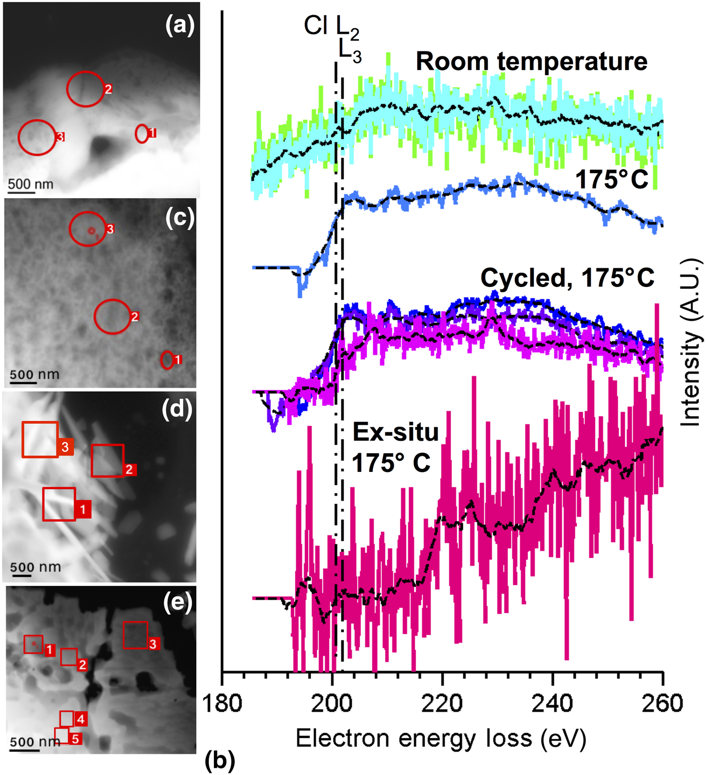
Figure 1 is a comparison of the elemental concentration of Cl before and after annealing FAPbI3−xClx at the optimal temperature of 175 °C in both a closed- in situ and open-cell ex situ environments based on collected and quantified EEL spectra starting at room temperature. Figure 1(a) is the collected HAADF image taken from unconverted and drop casted FAPbI3−xClx inside the differentially pumped and heated in situ gas cell. Figure 1(b) are the raw normalized and quantified Cl L2,3 EEL spectra that track the presence of Cl (<3 at%) for the as-deposited, sealed, and open-cell environments.
In situ STEM microscopy and spectra collected of heated FAPbI3−xClx films in an environmentally controlled gas cell. (a) Starting at room temperature FAPbI3−xClx was studied and probed using STEM-based EELS. (b) The Cl L 2,3 EELS ionization edge at 200 eV was sparsely acquired from samples annealed at different conditions. (c) In situ heating at 175 °C was applied in a rapid one step anneal for 10 min under identical conditions. Following the one-step anneal the Cl L 2,3 edge was collected and quantified from three separate areas, and found to be homogenously mixed throughout on the order of 2.3 ± 0.3 at%. (d) Multiple annealing steps at 175 °C shows the addition of oriented growth and similar chlorine retention with near identical atomic percentages (1.8 ± 0.3 at%). (e) Comparing with converting perovskite in ambient air however, we imaged a difference in morphology and a clear lack of chlorine measured from multiple areas.

Converting FAPbI3−xClx in one rapid step at 175 °C, Fig. 1(c) shows the conversion to a nanoporous material, where measuring Cl with EELS from multiple areas shows retention up to the same atomic percentage, <3 at%. The measured Cl-L 23 spectra reported is consistent with the previous reported L edge EEL spectra by Senga et al. showing Cl L-edge atomic spectra from cesium chloride (CsCl).[Reference Senga and Suenaga26] Well documented in the literature is the radiation sensitivity of Cl to electron beams.[Reference Egerton, Li and Malac27] In the literature there is further a lack of studies reporting on the fine structure associated with different physical states of Cl. In light of the radiation sensitivity and clear lack of theoretical fine structures, using EELS to determine the physical state is difficult at this time. Based on the EELS measurements so far, we therefore expect Cl to be retained in the structure as a low concentration (<3 at%) dopant that assists in the crystallization of the perovskite. In the next sections, we will report on Cl in detail over several grain boundaries and grain interiors using STEM and XRD to assert the presence and distribution in converted films.
Under these same in situ conditions FAPbI3−xClx was rapidly annealed over 10 thermal cycles in the presence of flowing inert nitrogen gas. One complete cycle is defined as starting at 50 °C, holding at 50 °C for 3 min, raising the temperature to 175 °C within 2 min (62.5 °C/min), holding for 5 min at 175 °C, and returning to 50 °C. This results in a 10-min total cycle duration. Keeping in mind the thermal mass of material within the cell is minimal compared with benchtop 1 cm2 cell growth, the relative measures of time and near immediate conversion need to be concerned relative when scaling to cover larger areas. Following two temperature cycles for a total of 20 min, Fig. 1(d) report the material retains Cl. This is iterated in the EEL spectra labeled “cycled” in Fig. 1(b) collected from different areas of the sample. The average reported Cl concentration is 1.8 ± 0.3 at% from these three areas. Temperature-cycling FAPbI3−xClx inside a closed cell dry environment therefore does not appreciably degrade (<1 at%) the annealed material chemistry.
Annealing FAPbI3−xClx by opening the cell to ambient air, containing water vapor at 175 °C and measuring the structure and chemistry with STEM shows a significant departure in the material chemistry from the in situ closed cell studies. In the STEM image Fig. 1(e), we observe a polycrystalline material with larger grains, which is a significant deviation from the one-step and thermal cycled in situ converted closed cell perovskite material. The larger grains are in agreement with the current literature following annealing perovskites in the presence of water vapor.[Reference Christians, Miranda Herrera and Kamat17, Reference Lv, Pang, Zhou, Padture, Hu, Wang, Zhou, Zhu, Zhang, Huang and Cui19] Measuring the Cl L 2,3 edge in Fig. 1(b) shows a clear lack of the principal leading edge. The absence of Cl following heating in the presence of water vapor in ambient air, we presume, as others is correlated with the sublimation of the organic cations (FACl) or HCl.[Reference Chen, Zhou, Fang, Stieg, Song, Wang, Xu, Liu, Lu, You, Sun, McKay, Goorsky and Yang12, Reference Unger, Bowring, Tassone, Pool, Gold-Parker, Cheacharoen, Stone, Hoke, Toney and McGehee20, Reference Grancini, Marras, Prato, Giannini, Quarti, De Angelis, De Bastiani, Eperon, Snaith, Manna and Petrozza28] The existence of residual water vapor trapped at grain boundaries has been reported in our previous studies, and suggests this also provides a pathway for subsequent desorption of the halide species.[Reference Aguiar, Wozny, Holesinger, Aoki, Patel, Yang, Berry, Al-Jassim, Zhou and Zhu25] The result is consistent with current device studies that state after conversion there is no trace of Cl in their final devices.[Reference Starr, Sadoughi, Handick, Wilks, Alsmeier, Kohler, Gorgoi, Snaith and Bar29] Based on comparing an open and closed cell environment, we report only under sealed conditions is Cl retained. Our findings suggest that there is a need to further optimize growth protocols associated mixed halide perovskites to consider retaining Cl and room temperature partial crystallinity, which we will be discussed in the next section.
In summary, the effect of Cl on conversion to a polycrystalline material measured inside the in situ environmental cell is consistent with a reaction involving escaping vapor upon heating. Annealing the perovskite in a dry nitrogen environment at 175 °C produces perovskite crystals with comparable morphologies relative to device-ready films. Unlike the pure halide perovskite system, utilizing a Cl containing perovskite precursor solution resulted in poor device performance when films were processed in a rapid one-step 175 °C anneal. However, it is useful to note that we correlate majority of the poor device performance with poor film coverage and small grain morphology rather than possible Cl loss during dry air annealing.
Chemical and structural imaging of converted FAPbI3−xClx
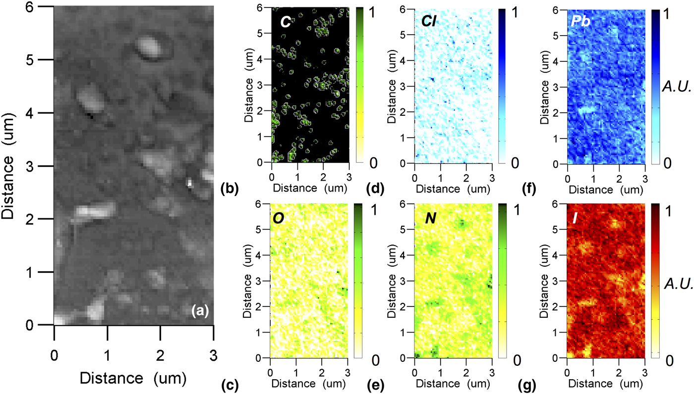
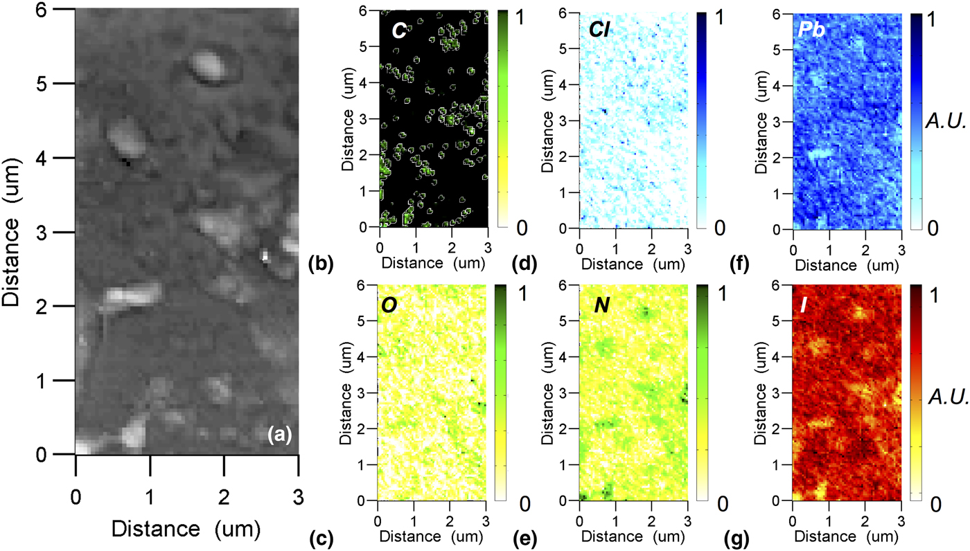
Iterating on the chemistry of these films, we performed chemical imaging using STEM-based x-ray energy-dispersion spectroscopy (EDS). At room temperature, a 3 × 5 µm area was imaged in Fig. 2(a) with atomic contrast dark field STEM imaging. The micrograph reveals individual micron size precipitates in the converted material. A closer look with STEM-based EDS chemical imaging presents the distribution of [Fig. 2(b)] C, [Fig. 2(c)] O, [Fig. 2(d)] Cl, [Fig. 2(e)] N, [Fig. 2(f)] Pb, and [Fig. 2(g)] I. Correlating atomic contrast image and these chemical maps, reveals that the precipitates are mostly Pb, N, and I containing. Each of these maps are qualitative or semi-quantitative at best given each is based on a standardless net count quantification. The distribution of Cl shows clear spots that are not consistent with the presence of Pb or I, but found mostly within the bulk of the material.
(a) STEM image taken at room temperature and after conversion at 175 °C. Standardless EDS chemical images were collected and semi-quantified to arbitrary units for (b) C, (c) O, (d) Cl, (e) N, (f) Pb, and (g) I. Profiles are provided at room temperature of converted FAPbI3−xClx. The profiles are normalized by residual net counts after a complete background subtraction and standardless quantification. The maps are qualitative if not semi-quantitative at best.
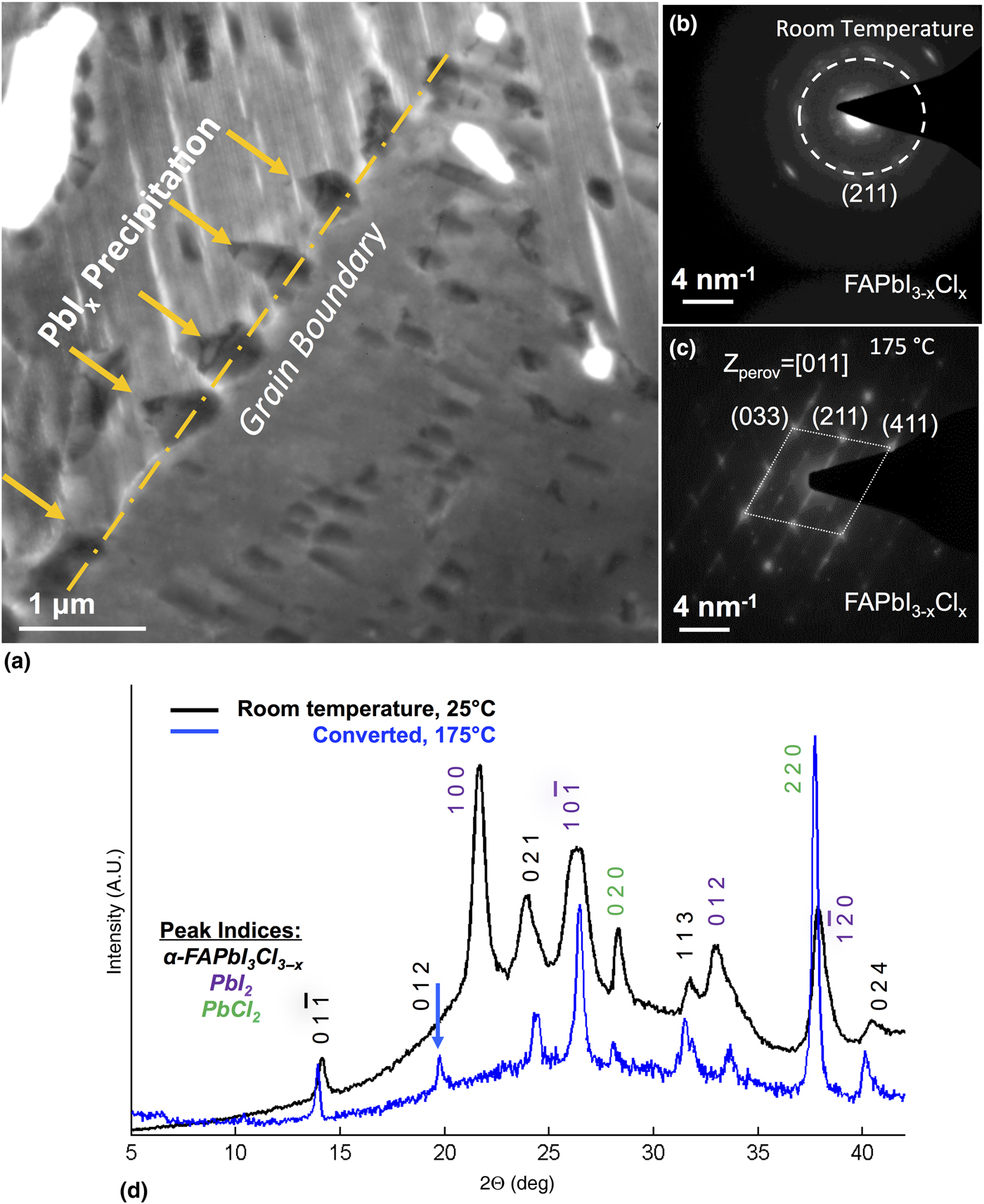
Over the FAPbI3−xClx films, we turn our attention to the crystal structure before and after conversion. Figure 3(a) is a TEM micrograph taken over an area containing a grain boundary. There is a clear preference for intergranular precipitation, where there is enough free volume at the grain boundary to support growth. The same precipitation pattern and chemistry previously reported in Aguiar et al. is found.[Reference Aguiar, Wozny, Holesinger, Aoki, Patel, Yang, Berry, Al-Jassim, Zhou and Zhu25] Figure 3(b) is a collected selected area diffraction pattern prior to conversion. The pattern reports partial crystallinity, where there are visibly weaker diffraction spots corresponding to the (211) lattice diffraction spots of perovskite. The partial crystallinity at room temperature has been previously reported in detail.[Reference Zhao and Zhu11, Reference Lv, Pang, Zhou, Padture, Hu, Wang, Zhou, Zhu, Zhang, Huang and Cui19] Compared with the fully converted film Fig. 3(c), reveals the same spots, but under strongly diffracting conditions reveals no apparent unconverted rings. Visible in this selected area pattern are also weaker spots corresponding to the crystalline structure of PbI2. We note only PbI2 peaks are observed in these patterns and chlorinated phases are not found in these smaller area patterns.
(a) TEM image taken after conversion at 175 °C centered at a grain boundary. Imaging reveals both converted perovskite and the presence of PbI2 precipitation. Structure is confirmed following collecting selected area electron diffraction patterns (b) before and (c) after conversion at 175 °C. Indexing the peaks found in each of the diffraction corresponds to a partial to full crystallization of the films. (d) Complementary XRD profiles taken at room temperature and after conversion at 175 °C. Scans are provided at room temperature (black line) and compared with a converted perovskite (blue line) at 175 °C. The superimposed profiles are further indexed in the vertical text that corresponds to the cubic perovskite (black), PbI2 (purple), and PbCl2 (green).
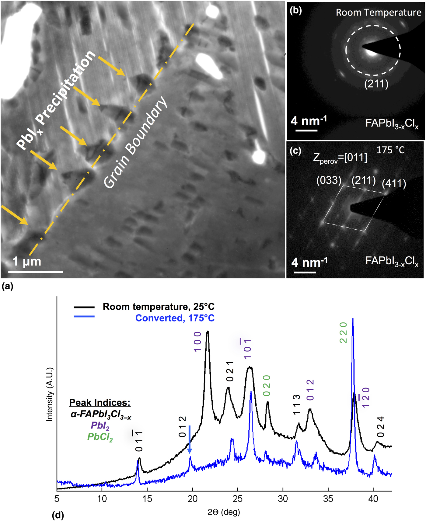
Over a larger area, XRD reveals the presence of chlorinated phases, potentially at lower concentrations. Measuring and comparing the same films in Fig. 3(d) at room temperature and at 175 °C with in situ XRD reports partial to full crystallinity at higher temperatures. The Miller indices are provided for the FAPbI3−xClx perovskite cubic phase, while “PbI2” and “PbCl2” phases are also labeled for the lead iodide and the starting perovskite phases at room temperature. The XRD data collected at room temperature, 25 °C, shows peaks originating from the cubic phase superimposed on an amorphous background profile, centered roughly at 26°, originating from the soda lime glass substrate. The film is highly textured and therefore the intensities of the peaks are not fitted against expected structure factors. From room temperature to 175 °C, the precursors react to further crystallize into the FAPbI3−xClx perovskite cubic phase, where the (100) peak corresponding the PbI2 phase is lost in the conversion and subsequent heating. Phase separation of the PbI2 and PbCl2 phases are observed at room temperature and 175 °C. The PbI2 phase can be indexed to a cubic-type crystal structure belonging to the P-3m1 space group, and PbCl2 is indexed to a cubic primitive unit cell corresponding to a = 6.7463 Å and b = 4.6332 Å, α = δ = β = 90° unit-cell dimensions. The FAPbI3−xClx phase can be indexed to a perovskite alpha phase type crystal structure belonging to the P-3m1 space group. Based on these diffraction profiles, we show that FAPbI3−xClx partially crystallizes in the proximity of room-temperature, 25 °C. We suspect as others have reported the lower partial crystallization temperature is due to the incorporation of Cl and is indicative of supplying a bonding element that can effectively passivate bonds, acting as a crystallizing agent.[Reference Lv, Pang, Zhou, Padture, Hu, Wang, Zhou, Zhu, Zhang, Huang and Cui19]
Controlling film morphology of FAPbI3−xClx
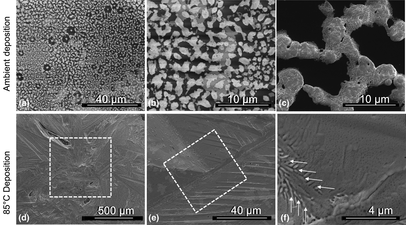
Based on the previous series of in situ measurements, annealing in ambient air leads for a tendency for chemical desorption of Cl, presumably mediated by the presence of water vapor during heating. Furthermore, FAPbI3−xClx crystallizes at lower temperature with partial crystallinity approaching room temperature.[Reference Zhao and Zhu11, Reference Lv, Pang, Zhou, Padture, Hu, Wang, Zhou, Zhu, Zhang, Huang and Cui19] Both of these key observations led to changes in device growth strategies of FAPbI3−xClx over other organic inorganic PSCs. To produce high coverage FAPbCl3−xI3 films that address the partial crystallinity at room temperature the drop casting procedure needs to be modified.[Reference Nie, Tsai, Asadpour, Blancon, Neukirch, Gupta, Crochet, Chhowalla, Tretiak, Alam, Wang and Mohite30] In an effort to on the coverage of FAPbCl3−xI3 films during drop casting, we compare the effect of changing the film growth wetting contact angle by changing the temperature of the substrate in Fig. 4 under dry conditions. Comparing scanning electron microscopy (SEM) micrographs taken of ambient room temperature casted FAPbI3−xClx [Figures 4(a–c)] with hot casted films at 75 °C [Figures 4(d–f)], show a clear difference in surface texture. The difference in ambient temperature and hot casting FAPbI3−xClx is with temperature we can effectively tune the wetting film contact angle and shape. At room temperature, the film contact angle is greater approaching a spherical droplet, were at higher temperature we are attaining a greater degree of surface wetting. Effectively raising the substrate temperature can tune the angle by adjusting the interfacial energies between the wet dropped film and the heated substrate. There is a clear correlation that raising the temperature from ambient to less than 100 °C (below the crystallization temperature) is necessary to improve film coverage for FAPbI3−xClx and ultimately improve on device efficiency.
(a–c) Collected SEM images compare the surface coverage and film growth between ambient drop casting and (d–f) hot casting of FAPbI3−xClx on compact titania treated SiNx. Based on the comparison of ambient and hot drop casting, we applied heated drop casting under controlled ambient dry conditions (low relative humidity) to fabricate our solar cells. The arrows indicate the domain growth direction, where a grain boundary is forming.

Device growth
FAPbI3−xClx solar cells were fabricated in a dry air filled dry box with less than 10% relative humidity, with film coverage over a 1 cm2 area following hot casting at 75 °C. The FAPbI3−xClx films examined here are polycrystalline containing the standard planar architecture with Ag, spiro-O-MeTAD, perovskite, and c-TiO2, and FTO as the front contact, HTM, absorber, compact layer and back contact, respectively. One of the key observations from the in situ studies is that we show optimized processing of FAPbI3−xClx in a dry environment that includes minimizing the amount of residual water vapor present. Therefore, the perovskite devices fabricated for this study were produced in a dry air environment in an attempt to reduce and mitigate the interaction of Cl with water vapor. The typical device photocurrent density-voltage J–V curve has a best short-circuit current density (J sc) of 18.93 mA/cm2, open-circuit voltage (V oc) of 0.96, fill-factor (FF) of 0.66, and a final photoconversion efficiency (η) of 12.07% (see Fig. S1). The mixed halide devices are affected by hysteresis which is consistent with other reported mixed halide devices in the literature. The device averages and standard deviations are reported in the supplementary information (see Table S1), showing that the J sc, V oc, FF, and η are relatively stable over 10 devices.
Conclusion
The key observation from our studies is that we show superior processing of FAPbCl3−xI3 in a dry environment, similar to FAPbI3. The presence of any water vapor in processing FAPbCl3−xI3 can lead to the loss of the halide in the final perovskite crystals following sublimation. These results confirm current speculation in the literature and our previous work. We present the addition of a halide element that not only leads to a change in the rate of converting perovskite, but can only otherwise be retained in the final material if the surrounding environment contains minimal water vapor. Chlorinated bonds with the surrounding elemental constituents are tenuous at best and can be easily broken by the presence of residual water vapor and lost to the environment following sublimation. This study concludes in order to retain Cl there is a need to address benchtop device growth protocols to improve upon the final material chemistry of halide incorporated perovskite solar cells.
Supplementary Material
The supplementary material for this article can be found at https://doi.org/10.1557/mrc.2017.52
Acknowledgments
This work was supported by the National Renewable Energy Laboratory as a part of the Non-Proprietary Partnering Program under Contract No. DE-AC36-08-GO28308 within the U.S. Department of Energy. TGH and the hot-stage in situ STEM work were supported by the U.S. Department of Energy, Office of Science, Basic Energy Sciences, Materials Sciences, and Engineering Division under grant number 2013LANL8400.