

DISCUSSION POINTS
-
• How can manufacturing costs for renewable energy systems be reduced?
-
• Will the advances in high-power lasers lead to lower cost for renewable energy material processing?
-
• What is the role of high-power lasers for material processing in solar cell manufacturing?
Introduction
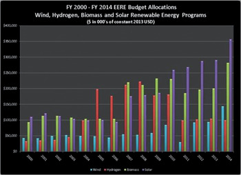
There is a growing interest in renewable energy sources 1 such as solar, wind, biofuels, geothermal, etc. to meet the escalating energy needs and concern for environmental changes. Figure 1 shows the U.S. Department of Energy EERE budget allocations for various renewable energy sources from 2000 to 2014. The renewable energy sources are attractive but the cost of energy generation must be further lowered to be competitive with other sources of energy. The laser processing of materials has the potential to lower the manufacturing cost. High-power lasers are already used in various manufacturing sectors such as aerospace, microelectronics, biomedical, automotive, and general manufacturing, and are expected to play an important role in various renewable energy applications. This review article examines the current state of the art for various applications of high-power lasers in the renewable energy area and discusses the future outlook.
Budget allocations on renewable energy programs in the US from 2000 to 2014. 1

High-power lasers provide a noncontact method of delivering energy at selected locations. The laser beam can be focused to micrometers in size, thus allowing microscale processing of materials. The direct writing capability enabled by high-power lasers may allow for the elimination of a costly photolithographic processing step. Laser light can be absorbed near the surface region, and so is ideally suited for surface modification and annealing without heating the entire object and hence providing substantial savings in the thermal budget. The significant advances in high-power lasers with the attainment of tens of kilowatts of optical power, high repetition rates (>MHz), reduction in size, low cost per photon (<1$/watt), and high optical power conversion efficiency (>30%) are driving the use of lasers for material processing with very high throughput.
Fundamentals of laser material interactions
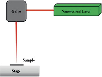
In laser material interactions, Reference Kannatey-Asibu2 the light is absorbed by the material and raises its temperature. An experimental setup for laser processing is shown in Fig. 2. If the laser energy density is high enough, it can cause melting and vaporization. Most laser processing techniques are based on thermal effects. The amount of laser light absorbed can be calculated from the optical constants of the material at a given laser wave length. The thermal effects can be calculated using the heat equation.
Laser setup with a galvanometer that can control laser scanning in 2D directions for transfer, doping, and ablation processes.

Optical and thermal modeling
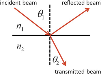
In laser processing of materials, when the laser light is incident on the material surface (as shown in Fig. 3), a portion of the laser light is reflected, a portion is absorbed, and in some cases it may be partially transmitted. The amount of light reflection can be calculated using the optical constants n, k of the material, where n is the refractive index and k is related to absorption. For normal incidence, the surface reflection ( R ) and transmission ( T ) are given by 3 :
 $${\rm{Normal}}\,{\rm{incidence}},\,R = {{{{\left( {{n_1} - {n_2}} \right)}^2}} \over {{{\left( {{n_1} + {n_2}} \right)}^2}}};\,T = {{4{n_1}{n_2}} \over {{{\left( {{n_1} + {n_2}} \right)}^2}}}\quad .$$
Light reflection and refraction at the interface.

When light is incident at an angle, the polarization state of the incident light must be considered. For S-polarized light:
 $${R_{\rm{S}}} = {{{{\left( {{n_1}\cos {\theta _1} - {n_2}\cos {\theta _2}} \right)}^2}} \over {{{\left( {{n_1}\cos {\theta _1} + {n_2}\cos {\theta _2}} \right)}^2}}};\,{T_{\rm{S}}} = {{4{n_1}{n_2}\cos {\theta _1}\cos {\theta _2}} \over {{{\left( {{n_1}\cos {\theta _1} + {n_2}\cos {\theta _2}} \right)}^2}}}\quad .$$
For P-polarized light:
 $${R_{\rm{P}}} = {{{{\left( {{n_2}\cos {\theta _1} - {n_1}\cos {\theta _2}} \right)}^2}} \over {{{\left( {{n_2}\cos {\theta _1} + {n_1}\cos {\theta _2}} \right)}^2}}};{\rm{\ }}{T_{\rm{P}}} = {{4{n_1}{n_2}\cos {\theta _1}\cos {\theta _2}} \over {{{\left( {{n_1}\cos {\theta _2} + {n_2}\cos {\theta _1}} \right)}^2}}}\quad .$$
For electrically conducting media the index will be complex,
 $\tilde n$
= n + ik, where k
1 = 0 for the incident media and k
2 = k and reflectance for normal incidence will be given by
 $$R = {{{{\left( {{n_2} - {n_1}} \right)}^2} + {k^2}} \over {{{\left( {{n_2} + {n_1}} \right)}^2} + {k^2}}}\quad .$$
From tabulated n and k values, surface reflectance can be calculated. For normal incidence on metals with conductivity σ and incident light frequency ω it can be approximated as Reference Born and Wolf4 :
 $$R = 1 - 2\sqrt {{{2{\varepsilon _0}\omega } \mathord{\left/ {\vphantom {{2{\varepsilon _0}\omega } \sigma }} \right. \kern-\nulldelimiterspace} \sigma }} \quad .$$
For Cu metal, σ = 6.7 × 10⁷ (Ω m)−1 and ω = 7 × 10¹⁴ so R = 0.97. The light absorption is given by Beer's law: I(z) = I 0e−αz where absorption coefficient α = 4πk/λ, I 0 is the incident light intensity and z is the material thickness. For laser processing, the calculation of surface reflectivity is important as it determines the amount of light coupled into the material.
The following equation describes the thermal behavior of the material under laser irradiation:
 $${{\partial H} \over {\partial t}} = \nabla \cdot\left( {k\nabla T} \right) + S\quad ,$$
where T is the temperature, H is the enthalpy, k is the thermal conductivity of the material, and S is the energy deposited by the laser heating source. The source term can be written as Reference Kannatey-Asibu2 :
 $$S = {I_0}\left( t \right)\left( {1 - R} \right)\alpha {{\rm{e}}^{ - \alpha z}}\exp \left( {{{ - {r^2}} \mathord{\left/ {\vphantom {{ - {r^2}} {{a^2}}}} \right. \kern-\nulldelimiterspace} {{a^2}}}} \right)\quad ,$$
where α is the light absorption coefficient, R is the surface reflectance, I 0 is the laser intensity, r is the radial distance, a is the laser beam radius, and z is the light penetration depth. The solution of the nonlinear thermal equation requires numerical methods. There are commercial codes like COMSOL, ANSYS, Fluent, etc. that can provide the rise in temperature and its distribution. From the laser wave length, power, pulse duration and repetition rate, beam size, it is possible to calculate various parameters of interest.
Advances in high power lasers
Recently, significant progress has been made in high-power laser technology in terms of bringing down the cost per photon, availability of very high continuous wave (CW) and pulsed power lasers, and high wall plug efficiency. 5 Some of the key high-power laser types include: diode lasers, fiber lasers, solid state lasers, and disk lasers. Also, significant progress has been made in laser beam delivery systems using optical fibers.
Diode lasers
Diode lasers are based on direct band gap semiconductors like GaAs with a p–n junction, and output wavelengths are in the range of 785–1060 nm. A single junction can generate watts of optical power and by arranging them to form bars or arrays it is possible to achieve kilowatts of optical power. The electrical to optical power conversion efficiency is very high (>30%) and they are highly reliable with lifetimes of over 50,000 h. Though the beam quality of high-power diode lasers is relatively poor, they are available with fiber delivery. Diode lasers can be CW or pulsed with modulation rates of up to 50 kHz. 5
Fiber lasers
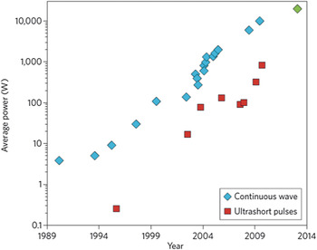
Fiber lasers are produced by coupling optical fiber and semiconductor lasers. 6 The beam from a diode laser is coupled into optical fibers containing rare earth doped ions to generate the light which remains inside the fiber. The fiber laser provides high beam quality (M 2 < 1.5, where M 2 is the beam quality factor, which compares the laser produced beam to an ideal Gaussian laser beam with M 2 = 1), and high optical powers (over 20 kW) at relatively low cost. Fiber lasers are compact, need little maintenance, have high wall plug efficiency, and exhibit long operational life. They are extensively used in various applications such as material processing, scientific research, and medical applications, and can be easily integrated for robotics applications. With Q-switch technology, the fiber lasers can provide CW as well as pulsed operation with pulse width in the range of 1–400 ns. The peak power can be in megawatts (MW) and pulse energy over 50 mJ. Figure 4 shows the evolution of fiber laser technology. Reference Jauregui, Limpert and Tunnermann7
Evolution of the average output power of nearly diffraction limited fiber lasers (emitting either a CW or ultrashort pulses) over the past 25 years. Reference Jauregui, Limpert and Tunnermann7

Optical beam delivery systems
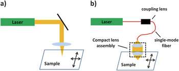
For material processing, the laser beam needs to be focused on the object. The beam can be delivered in two ways: one by free space optics using mirrors and lenses and second by fiber optics. A fiber optic beam delivery is commonly used to provide a collimated beam which can be focused with an external lens on the object as shown in Fig. 5. Fiber beam delivery systems use flexible cables. Laser beams can be focused to 10–20 µm in size, allowing the generation of very high power densities. A laser beam is coupled into the single mode or multimode fiber and beam can be delivered away from the laser source. The output of the laser beam is collimated by a lens and then focused by another lens on the materials to be laser processed.
(a) Free space delivery system and (b) fiber optic beam delivery system.

Laser applications for crystalline silicon solar cells
Introduction
While lasers are currently used by some manufacturers during the processing of crystalline silicon solar cells, the most widespread application of laser technology in the field of photovoltaics (PVs) is the scribing of thin-film solar cells to make large-area, series-connected PV modules (Section “Laser processing for thin film solar cells”). Most thin-film solar cell manufacturers utilize laser scribing for at least part of the interconnection process as the thin-film cells are patterned and series-connected into large-area monolithic modules.
Some laser processes for crystalline silicon solar cells, such as laser edge isolation (Section “Laser edge isolation”) and laser grooving for selective emitter formation (Section “Laser marking, grooving, and cutting”), were technically successful, but have generally been replaced by less expensive alternatives. A laser marking process is currently being utilized by some crystalline silicon solar cell manufacturers for single wafer identification to assist in quality control and process improvement (Section “Laser marking, grooving, and cutting”).
However, new laser technology is actively being investigated by a number of prominent research organizations for the processing of crystalline silicon solar cells. Reference Bogue8–Reference Booth17 Lasers are being used to form both emitter and ohmic contacts for crystalline silicon solar cells using processes such as laser doping (Section “Laser doping”), laser-fired contacts (LFCs) (Section “Laser-fired metal contacts”), laser transfer processes (Section “Laser transfer”), and laser ablation of dielectric passivation layers (Section “Laser ablation of dielectric passivation layers”). In addition, several organizations are utilizing laser drilling of vias (holes) in silicon wafers for metal-wrap-through (MWT) and emitter-wrap-through (EWT) back-contact solar cells (Section “Laser drilling”). Also, lasers are being used to form low-reflectivity microtextured surfaces (Section “Light trapping by laser microtexture”) and to form thin crystalline silicon films by laser crystallization of amorphous silicon films (Section “Other laser processing: annealing, sintering, crystallization, defect repair”).
Laser edge isolation
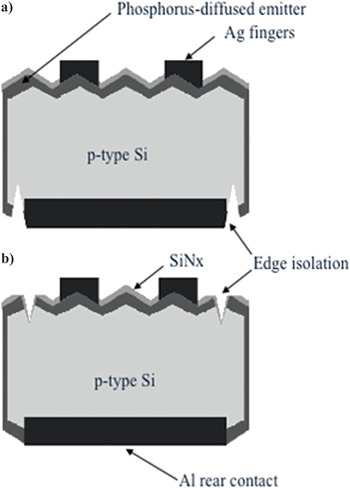
The p–n junction in most crystalline silicon solar cells is formed by diffusing phosphorus into a p-type wafer at temperature of ∼850 °C using POCl3 gas as a dopant source. This process usually results in the creation of a leakage path (or shunt) from the front surface emitter to the rear surface base contact due to diffusion of phosphorus into the edges of the wafer and some wrap-around of diffused phosphorus onto the rear surface. A pulsed laser can be used to scribe an isolation groove around the outer periphery of the top or rear surface (see Fig. 6), effectively removing the shunt path. Reference Hauser, Hahn, Spiegel, Feist, Breitenstein, Rakotoniaina, Fath and Bucher18 This is usually accomplished using a Q-switched Nd:YAG or Nd:YVO4 laser operating in the infrared wave length to scribe a narrow isolation groove or trench near the edge of the emitter on the top surface of the wafer as shown in Fig. 6(b). The isolation groove is about 10–30 μm deep and 40–80 μm wide and is placed as close to the edge of the wafer as possible to maximize the solar collection area. Reference Dunsky19
Schematic of silicon solar cells with laser isolation grooves on (a) the rear surface and (b) on the front surface. Reference Carlson10

However, in recent years, many manufacturers are replacing laser edge isolation with a single-sided wet etching process since although the etching process requires the handling of hazardous materials, it appears to be more cost effective. Reference Hofmann, Schmidt, Kohn, Rentsch, Glunz and Preu20
Laser doping
The depth of p–n junctions in silicon solar cells is typically less than a micrometer, and laser-induced diffusion is ideally suited for forming shallow p–n junctions in silicon. Fairfield and Schwuttke Reference Fairfield and Schwuttke21 were the first to demonstrate laser doping of silicon when they used a laser to create a p–n junction in silicon in 1968. In their work, a polished silicon wafer was coated with phosphorus and scanned with a pulsed laser beam.
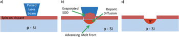
In an example of more recent laser-doping work, Reference Ventura, Schunck, Muller, Barthe, Vetrella, Pirozzi and Salza22 a spin-on-dopant solution is first spin coated on a silicon surface. The coated silicon surface is then exposed to laser illumination, and above a certain laser fluence or energy density, the silicon surface can be melted. The emitter dopant from the spin-on-dopant film will diffuse into the molten silicon to form the junction. The schematic of the process is shown in Fig. 7. The advantage of this approach is that the selective doping can be achieved with a direct laser write process without requiring photolithography. Also, in the laser doping process, only the silicon surface is heated, so it minimizes the incorporation of impurities and reduces the thermal budget. However, for large area applications of laser doping, the throughput needs to be optimized with larger beam size using high-power lasers or multiple laser beams.
Laser doping process: (a) Step 1: laser pulse irradiation; (b) step 2: molten pool formation and dopant diffusion; (c) junction formation.

Laser-fired metal contacts
High-performance solar cells with efficiencies as high as 21.7% Reference Schneiderlochner, Preu, Ludemann and Glunz23 have been fabricated by scientists at Fraunhofer ISE using a laser firing process, which is a variant of laser doping. Reference Hofmann, Saint-Cast, Suwito, Seiffe, Schmidt, Kambor, Gautero, Kohn, Nekarda, Leimenstoll, Wagenmann, Erath, Catoir, Wolke, Janz, Biro, Grohe, Rentsch, Glunz and Preu24 The laser firing process involved forming localized p+ contacts by first depositing a passivation layer on the rear surface of a silicon wafer followed by the deposition of a layer of aluminum. The Al layer was then fired through the passivation layer using a Q-switched Nd:YAG laser with a wave length of 1064 nm. The laser pulse locally disrupts the dielectric passivation layer, melts the underlying Si, and allows Al to diffuse into the molten Si forming a localized p+ contact. The rear surface passivation layers in these high-performance cells consisted of ~70 nm of amorphous silicon (a-Si:H) covered with ~100 nm of SiO x . Both layers in the stack were deposited by plasma-enhanced chemical vapor deposition (PECVD). Reference Schneiderlochner, Preu, Ludemann and Glunz23
LFCs have also been made using other dielectric passivation layers such as thermally-grown silicon dioxide Reference Schneiderlochner, Preu, Ludemann and Glunz23 ; PECVD silicon nitride (SiN x :H) Reference Schneiderlochner, Preu, Ludemann and Glunz23 ; PECVD silicon carbide (SiC x :H) Reference Hofmann, Kambor, Schmidt, Grambole, Rentsch, Glunz and Preu25 ; PECVD silicon oxide (SiO x :H) Reference Hofmann, Kambor, Schmidt, Grambole, Rentsch, Glunz and Preu25 ; stacks of PECVD SiO x :H, SiN x :H, and SiO x :H Reference Hofmann, Kambor, Schmidt, Grambole, Rentsch, Glunz and Preu25 ; PECVD aluminum oxide (AlO x ) Reference Saint-Cast, Kania, Billot, Weiss, Hofmann, Gautero, Kohn, Biro, Rentsch and Preu26 ; and atomic layer deposited (ALD) AlO x capped with PECVD AlO x . Reference Saint-Cast, Kania, Billot, Weiss, Hofmann, Gautero, Kohn, Biro, Rentsch and Preu26 LFCs have also been made with different forms of Al. Most LFCs have been made using evaporated Al Reference Schneiderlochner, Preu, Ludemann and Glunz23 or sputtered Al, Reference Nekarda, Reinwand, Hartmann and Preu27 but laser firing has also been performed using screen-printed Al paste or Al foil, Reference Nekarda, Hörteis, Lottspeich, Wolf and Preu28 and high efficiency (>20%) solar cells have been made using all these forms of Al.
While most of the LFC research has been performed using pulsed nanosecond Nd:YAG lasers operating at a wave length of 1064 nm, other pulsed nanosecond lasers such as ytterbium fiber lasers Reference Panek, Drabczyk, Kulesza and Zięba29 and Nd:YVO4 (Ref. Reference Fischer30) have been used. LFCs have also been formed using millisecond single-mode fiber lasers. Reference Raghavan, Blecher, Palmer, Reutzel and DebRoy31
In the vast majority of the published research, laser firing has been used to make ohmic base contacts for solar cells by firing Al into p-type Si wafers. However, solar cells have also been made by laser firing Al into n-type Si wafers and forming localized emitter contacts. Reference Glunz, Schneiderlöchner, Kray, Grohe, Hermle, Kampwerth, Preu and Willeke32,Reference Granek, Hermle, Fleischhauer, Grohe, Schultz, Glunz and Willeke33 Solar cell conversion efficiencies as high as 19.4% were obtained by laser firing Al through a thermal oxide on the rear surface of 100 Ω cm n-type Si wafers. However, the efficiency fell significantly to ~13.5% when 1 Ω cm n-type Si wafers were used. The difference in performance is due to injection-dependent recombination in a laser-induced damaged region surrounding the localized laser-fired emitters. Reference Granek, Hermle, Fleischhauer, Grohe, Schultz, Glunz and Willeke33 Simulations indicated that the damaged region extended ~5 μm beyond the laser-fired emitter region and that the minority carrier lifetime was reduced to ~0.3 μs within the damaged region. The effective lifetime is almost an order of magnitude greater in the 100 Ω cm silicon wafer since the device operates in the high-injection regime, and the recombination rate within the laser-induced damaged region is reduced by almost one order of magnitude. Reference Granek, Hermle, Fleischhauer, Grohe, Schultz, Glunz and Willeke33
LFCs have recently been made using materials other than aluminum. Antimony (Sb) was laser doped into n-type crystalline silicon by Takahashi et al. Reference Takahashi, Matsumoto, Murakami and Hayashi34 in 1985 to form a low resistance ohmic contact, but unlike the laser-firing process developed by Fraunhofer, there was no dielectric passivation layer on the surface of the silicon wafer. More recently, Song et al. Reference Song, Balaji, Kim, Choi, Ryu, Park, Ju, Lee, Lee, Lee, Lee and Yi35 laser fired Sb through a thermal oxide into n-type Si to form localized back-surface field contacts, and they fabricated solar cells with efficiencies as high as 17.2%. In even more recent work, He et al. Reference He, Hegedus, Das, Shu, Bennett, Zhang and Birkmire36 laser fired Al/Sb stacked layers through either silicon nitride or p-type amorphous silicon to make ohmic contacts to n-type Si, and they demonstrated efficiencies as high as 16.9% in interdigitated back-contact silicon heterojunction solar cells.
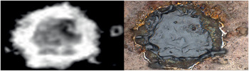
Interdigitated back-contact solar cells with efficiencies >18% were fabricated by laser firing a silver paste on the top of a dopant paste through a dielectric into n-type Si. Reference Sidhu, Bennett, Hmung, Ren, Zou, Carlson, Dong, Li, Lu, Song, Tao, Xia, Yang and Xing37 These back-contact solar cells exhibited good values of the open-circuit voltage (632 mV) and the short-circuit current density (39.7 mA/cm2), but the fill factors were limited to values ≤0.72 due to high series resistance. Imaging with a high-resolution, mid-IR thermal camera showed that resistive losses were occurring due to current crowding at both the laser-fired n+ and p+ contacts. Figure 8 shows both a thermal image and an optical microscope image of a laser-fired p+ contact. The thermal image shows nonuniform resistive heating under bias. The nonuniformities appear to be associated with variations in the topography and reflectivity of the Ag paste. In addition, most of the Ag paste has been removed from the central region of the laser-fired emitter due to laser ablation.
A thermal image (on the left) and an optical microscope image (on the right) of a localized laser-fired emitter made by laser firing a Ag paste over a dopant paste through an ALD AlO x /PECVD SiN x passivation stack.

The LFC process developed by Fraunhofer ISE is being commercialized by Hanwha Q-Cells for multicrystalline Si solar cells with passivated rear point contacts, and conversion efficiencies well above 18% have been demonstrated in a continuously running pilot line. Reference Kloter, Buss, Hussack, Kowalzik, Peters, Schutze, Stegemann and Muller38
Laser transfer
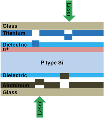
In the laser transfer process, a thin film on a substrate is transferred to the silicon surface. The laser-transferred film can be used to form a p–n junction or highly doped regions in silicon for metal contacts with low contact resistance. The laser-transferred film can also be used for patterning metal contacts on silicon solar cells. Figure 9 shows the laser transfer process using pulsed lasers. Reference Wang, Carlson and Gupta39 One of the advantages of the laser transfer process is that the transfer can be achieved selectively so that a photolithographic process is not required. The film transfer process can be achieved through a passivation dielectric layer, where the transferred film can make electrical contact to a silicon surface or can dope the silicon. Hoffmann et al. Reference Hoffmann, Röder and Köhler40 demonstrated that an antimony film could be laser transferred through an 80 nm silicon nitride layer and could form a selectively doped n+ layer in silicon.
Schematic of laser transfer process for contact formation on both the front and rear sides of a silicon solar cell. Reference Wang, Carlson and Gupta39

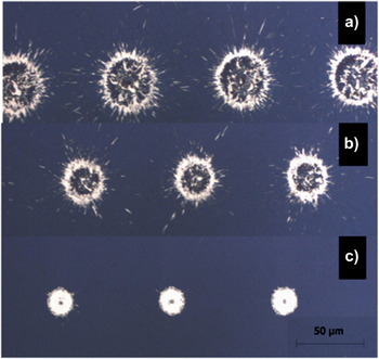
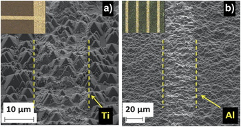
When a laser beam is incident on a thin film on a substrate, part of the light is absorbed by the film. The absorbed laser light energy raises the temperature of the film at the interface with the substrate and can cause melting and vaporization. The vapor pressure keeps rising since the vapor is contained in a small volume until a threshold value is reached where the surface tension cannot hold the molten region on the substrate. Then the metal film is transferred to the silicon surface due to the forward pressure generated at the metal film substrate interface. The vaporized metal in conjunction with the laser beam can locally melt silicon and can form an alloy with the molten silicon to generate ohmic contacts. Typical morphology of the transferred metal contacts is shown in Figs. 10 and 11. Reference Wang, Carlson and Gupta39 When high levels of dopants such as phosphorus are transferred, the dopant diffuses into p-type silicon to form a p–n junction or highly doped regions are formed for ohmic metal contacts in n-type silicon. For example, a thin film of a-Si doped with phosphorus deposited by CVD on a glass substrate can be laser transferred to silicon. Due to melting of silicon by the laser transfer process, a junction will be formed in silicon in a very short interaction time (typically on the order of a few tens to a few hundreds of nanoseconds) due to the fast diffusion of phosphorus in molten silicon.
Microscope images of transferred metal spots created by single laser pulses with different energy densities: (a) 1.1 J/cm2, (b) 0.90 J/cm2, and (c) 0.69 J/cm2. Reference Wang, Carlson and Gupta39

Scanning electron microscope (SEM) images of laser-transferred metal contacts on Si solar cell: (a) Ti contacts and (b) Al contacts. The insets are optical images of the transferred metal contacts. Reference Wang, Carlson and Gupta39

Laser ablation of dielectric passivation layers
Solar cells with efficiencies as high as 21.4% have been fabricated by using laser ablation of the rear dielectric passivation layer to form openings for localized contacts. A Nd:YVO4 laser operating at a wave length of 355 nm (pulse duration = 30 ns) was used to locally ablate a rear surface thermal SiO2 passivation layer over the boron- and phosphorus-diffused regions before applying the interdigitated finger metallization in an EWT solar cell. Reference Hermann, Engelhart, Merkle, Neubert, Brendemühl, Meyer, Harder and Brendel41
Das et al. Reference Das, Tous, Hernández, Jaffrennou, Ngamo, John, Posthuma, Baert and Poortmans42 also used a UV (355 nm) nanosecond Nd:YVO4 laser to ablate 80 nm of silicon nitride on the front surface of a textured Si surface with a 60 Ω/sq emitter to form openings for both point and line electroplated Ti/Cu contacts. They demonstrated conversion efficiencies as high as 18.55% using line contact ablation on full-size solar cells. Laser ablation can cause laser-induced damage at high-energy densities, but Correia et al. Reference Correia, Lossen, Wald, Neckermann and Bähr43 showed that nanosecond lasers could remove dielectrics such as SiO2 and silicon nitride from the surface of silicon wafers with phosphorus-diffused emitters with no significant laser-induced damage and minimal redistribution of the emitter dopant.
Hernández et al. Reference Hernández, Tous, Allebé, Philipsen, Schlenker, John, Baert and Poortmans44 used a UV (355 nm) nanosecond Nd:YVO4 laser to open contact vias in the silicon nitride antireflection coating on the front surface of cells made on p-type CZ-Si wafers. They also laser ablated openings in a rear surface oxide/nitride dielectric stack and then formed localized base contacts by depositing aluminum and firing. They obtained conversion efficiencies as high as 19.4% by contacting the emitter with a thin layer of Ti.
Laser drilling
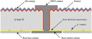
Lasers have also been used to drill arrays of small holes through wafers in the fabrication of MWT and EWT back-contact solar cells. In both types of cells, laser-drilled holes are used as vias to carry the current collected by the emitter on the front surface to busbars on the rear surface of the cell. In some cases, an emitter surface may also be formed over a portion of the rear surface of the Si wafer. In the MWT solar cell, a relatively small number of laser-drilled holes (~16 per wafer) are filled with metal and used to carry the photocurrent from a fine grid pattern on the front surface to busbars on the rear surface (see Fig. 12). In the EWT solar cell, a relatively large number of laser-drilled holes (∼15,000–25,000 holes per wafer) are formed and an emitter surface is formed on both the front surface and on the walls of the vias. In this case, there is no front surface grid and the conductivity of the emitter surface on the walls of the vias is sufficient to carry the collected front surface current to the busbars on the rear surface.
Schematic of a MWT solar cell.

Lee et al. Reference Lee, Lim, Kim, Moon, Seo, Lee and Cho45 used a single-mode Q-switched UV (355 nm) laser with a pulse duration of 40 ns for drilling holes for MWT silicon solar cells. Mingirulli et al. Reference Mingirulli, Grohe, Dohrn, Hofmann, Schubert, Roth, Biro and Preu46 used both a Nd:YAG laser (1064 nm wave length) with pulse durations in the range of 60–90 μs and a Yb:YAG laser (1030 nm wave length) with a pulse duration of 1 μs to drill holes in Si wafers for EWT silicon solar cells.
Lamers et al. Reference Lamers, Tjengdrawira, Koppes, Bennett, Bende, Visser, Kossen, Brockholz, Mewe, Romijn, Sauar, Carnel, Julsrud, Naas, de Jong and Weeber47 fabricated MWT solar cells on p-type multicrystalline Si wafers and demonstrated efficiencies as high as 17.9%. They laser drilled 16 holes in each wafer for the MWT connections that carried photocurrent from the fine grid pattern on the front surface to the busbars on the rear surface. Their final processing step involved using a laser to form an isolation trench around each hole and also around the edge of the cell. Drews et al. Reference Drews, Clement, Spribille, Thaidigsmann, Linse, Gutscher, Werner, Reitenbach, Ould Chighali, Wolf, Zimmer, Nekarda, Haedrich, Tranitz, Eitner, Wirth, Wilson, Biro and Preu48 fabricated MWT solar cells in a pilot line with efficiencies as high as 19.3% using a cell structure similar to that shown in Fig. 12.
Hermann et al. Reference Hermann, Engelhart, Merkle, Neubert, Brendemühl, Meyer, Harder and Brendel41 fabricated EWT cells (92 cm2) on float-zone Si with efficiencies as high as 21.4%. In addition to using lasers to drill the vias, they also used a picosecond Nd:YVO4 laser (wave length 532 nm) to ablate the rear silicon dioxide layer and form localized selective emitter contacts as well as localized contacts to the back-surface field regions.
Laser marking, grooving, and cutting
Laser ablation processes have been used by solar cell manufacturers to mark solar cells for identification, Reference Wanka, Rychtarik, Muller, Geissler, Kappe, Spallek, Vom Bauer, Ludwig and Wawer49 to form grooves in solar cells for selective emitters Reference Wenham and Green50 and to cut silicon ribbons into wafers. Reference Hanoka51
Solar cell manufacturers such as Q-Cells have used laser marking for single wafer identification, which improves quality control and assists in process improvement. Reference Wanka, Rychtarik, Muller, Geissler, Kappe, Spallek, Vom Bauer, Ludwig and Wawer49 Both Nd:YAG lasers (1064 nm) and Nd:YVO4 lasers (1064 nm) have been used to create dots ~100 μm in diameter and 10–30 μm deep (using 20–50 ns laser pulses) for marking silicon wafers.
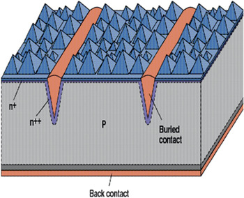
The laser-grooved buried contact solar cell was invented at the University of New South Wales Reference Wenham and Green50 and was commercialized by BP Solar in 1995. Reference Bruton, Heasman, Nagle, Cunningham, Mason, Russell and Balbuena52 Either a high-power Nd:YAG laser or a Nd:YVO4 laser operating in the infrared laser scribed grooves through both the antireflection layer and the shallow emitter of a textured p-type Si wafer (see Fig. 13). The grooves were typically about 30 μm wide and about 35 μm deep. After laser grooving, an additional phosphorus diffusion was used to form a heavily-doped selective emitter in the grooves. The rear surface and the grooves were then plated with Ni, Cu, and Ag. Efficiency as high as 18.3% was achieved in full-size Saturn cells (147.5 cm2) and efficiency over 20% was obtained in small area cells. Reference Bruton, Mason, Roberts, Hartley, Gledhill, Fernandez, Russell, Warta, Glunz, Schultz, Hermle and Willeke53 Manufacturing of the laser-grooved buried contact solar cell ceased in 2008 due to relatively high manufacturing costs compared to conventional screen-printed silicon solar cells.
A laser-grooved buried contact solar cell. Reference Bruton, Heasman, Nagle, Cunningham, Mason, Russell and Balbuena52

Lasers have also been used in production to cut silicon ribbons into wafers and to also mark the wafers for identification. Evergreen Solar developed a process to grow silicon ribbons using strings of refractory material, and they also developed an automated laser-cutting system to cut the silicon ribbon into wafers for cell processing. Reference Hanoka51 However, Evergreen Solar ceased commercial production of solar cells in 2011.
Light trapping by laser microtexture
The silicon surface of a typical smooth wafer reflects about 30% of sunlight due its high refractive index in the visible spectral region. For solar cells, surface light reflection needs to be minimized to achieve higher current density and hence higher solar cell efficiency. A quarter wave thick layer of a material such as Si3N4 or TiO2 on the top of a silicon surface can reduce the surface reflectance through its antireflection properties. These antireflection coatings are only effective at one given wave length. The solar spectrum is broad from the UV region to the near-infrared region, so antireflection coatings are not very effective for broad wave length sources.
Anisotropic chemical etching of silicon surfaces to generate surface microtexture has been used for light trapping applications. The chemically etched surface in combination with an antireflection layer has been shown to reduce the surface reflection to below 5%.
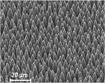
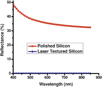
The silicon surface can also be microtextured to reduce surface reflection by pulsed laser processing. Under certain laser processing conditions, self-organized cone type microtexture can be formed on a silicon surface as shown in Fig. 14. The microtextured silicon (also called black silicon) shows very low reflectance (~1%) over broad spectral range as shown in Fig. 15. Reference Nayak, Iyengar and Gupta54 Solar cells with efficiency of over 16% have been demonstrated using laser microtextured silicon surfaces. Reference Nayak, Iyengar and Gupta55 The throughput of laser microtexturing process still requires improvement in order for this process to be cost effective.
SEM image of laser-microtextured Si surface. Reference Nayak, Iyengar and Gupta54

Light reflection from polished bare silicon and laser-microtextured silicon surface. Reference Nayak, Iyengar and Gupta54

Other laser processing: annealing, sintering, crystallization, defect repair
Alemán et al. Reference Alemán, Streek, Regenfuss, Glunz and Willeke56 used lasers to produce electrical contacts to the emitter of silicon solar cells by sintering metal powders. They spread metal powders such as silver, molybdenum, and tungsten on the top of the silicon wafer, and then used a laser beam to sinter the powder forming an electrical finger pattern contact to the emitter. After removing the nonsintered powder, they electroplated silver to increase the conductivity of the contacts. The electroplated fingers were 40 μm wide and 18 μm thick. They demonstrated conversion efficiencies of ~14.5% in small (1 cm2) p-type Si solar cells by laser sintering tungsten particles to a 50 Ω/sq emitter.
Lasers have also been used to repair defects present in the surface region of silicon solar cells. Abbott et al. Reference Abbott, Trupke, Hartmann, Gupta and Breitenstein57 used a Nd-YAG laser (1064 nm, 200 ns pulses) to ablate grooves to locally isolate shunted regions in industrial silicon solar cells. They were able to improve the performance of a shunted industrial screen-printed solar cell from a conversion efficiency of 9.6 to 13.3% by laser isolating shunts.
Lasers have been used to crystallize thin amorphous silicon films on glass to form a seed layer for the epitaxial growth of thicker Si films (>10 μm) for thin crystalline silicon solar cells. Nd:YAG lasers have been used in the CW mode to grow relatively large crystals (tens of micrometers wide and >100 μm long), Reference Andrä, Bergmann and Falk58 but the scanning speeds were not adequate for commercialization. In other works, Reference Nayak, Eaton, Selvan, McLeskey, Gupta, Romero and Ganguly59,Reference Andrä, Bochmann, Falk, Gawlik, Ose and Plentz60 the laser scanning speed was increased by first heating the a-Si coated borosilicate glass to 600 °C, and then scanning with a CW diode laser operating at a wave length of 806 nm. This approach allowed the scanning rate of a line-focused (30 mm × 0.1 mm) laser beam to be increased to several cm/s. Reference Andrä, Bochmann, Falk, Gawlik, Ose and Plentz60
Andrä et al. Reference Andrä, Höger, Bergmann, Gawlik, Plentz, Ose, Falk, Burghardt and Schippel61 used both a CW diode laser and a diode-pumped disk laser (512 nm, pulse duration 250–600 ns) to crystallize thin boron-doped a-Si films (60–400 nm thick) at 600 °C on borosilicate glass coated with silicon nitride. After increasing the thickness of the thin silicon films using epitaxy, they fabricated silicon solar cells with open-circuit voltages over 500 mV and short-circuit current densities as high as 20 mA/cm2.
Laser processing for thin film solar cells
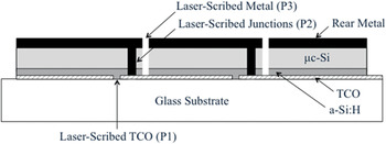
Lasers are widely used in the manufacturing of thin film solar cells. Reference Schoonderbeek, Schutz, Haupt and Stute62–Reference Slaoui, Chowdhury, Prathap, Said-Bacar, Bahouka and Mermet65 Laser scribing of thin film solar cells was first used to fabricate monolithic PV modules by performing three laser scribes to connect amorphous silicon (a-Si:H) solar cells in series. Reference Hank66,Reference Carlson and Pankove67 This process used a frequency-doubled pulsed Nd:YAG laser (532 nm) to first scribe a transparent conductive oxide (TCO) on a glass substrate into a series of thin conductive strips (the P1 scribe), ~1 cm wide (see Fig. 16). After depositing the thin film semiconductor junction (or junctions), the laser power density was adjusted to ablate only the semiconductor layers (P2 scribe) in a thin strip adjacent to the scribe in the tin oxide. After the rear contact metal (e.g., aluminum) was deposited, a laser scribe was performed with the light incident through the glass substrate to remove a thin strip of both the semiconductor materials and the rear metal contact (P3 scribe) completing the interconnection process. The PV module is then typically completed by laminating the laser-scribed panel to another sheet of glass using an encapsulant such as ethylene vinyl acetate (EVA) and then electrically connecting a junction box to the rear and mounting the panel in a frame.
Schematic of a laser-scribed tandem junction (a-Si:H/μc-Si) PV module. The a-Si:H and μc-Si layers consist of p–i–n junctions, where the interfacial region between the junctions functions as a tunnel or recombination junction. Reference Carlson10

The laser scribing process automatically connects all the thin strip solar cells in series as the metal rear contact of one cell is electrically connected to the tin oxide front contact of the adjacent cell. This allows the fabrication of a monolithic PV module that can be scaled up in size without increasing the thickness of any of the deposited layers. Some laser scribing systems consist of a high-power laser combined with optics that splits a single beam into 4 or 8 parallel laser beams allowing high-throughput processing. In addition to Nd:YAG lasers, some laser scribing systems use Nd:Vanadate lasers (10–60 ns pulse durations) operating at the fundamental (1064 nm) or first harmonic (532 nm) wave length with repetition rates up to 200 kHz. 68 High-speed scribing (400 cm/s) can be performed with galvo-based technology while linear axis drives are slower, but can provide higher accuracy.
The laser scribes are typically on the order of 20–40 µm in width and the spacing between the scribes may also be on the order of 30–40 µm leading to an interconnection region of about 120–200 µm in width. Reference Carlson and Arya69 Thus, for 1-cm-wide solar cell strips, only about 1.2–2.0% of the module area is lost due to the interconnection.
While CdTe and CIGS thin film PV modules have also been processed using laser systems similar to those mentioned above, the P2 and P3 scribes in CdTe modules have also been performed using picosecond fiber lasers. Reference Baird, Gerke, Wieland and Paudel70 In this case, both the CdS/CdTe scribe (P2) and the rear Cu/Au contact scribe (P3) were performed using a 30 ps laser (wave length of 532 nm) operating at a repetition rate of 200 kHz.
CIGS modules have generally been processed using a nanosecond laser (1064 nm wave length) to scribe the Mo electrode (P1 scribe), which is typically deposited on glass, while the patterning of the semiconductor material (CIGS/CdS) (plus an intrinsic ZnO layer) and the top transparent conducting oxide (ZnO) have typically been performed by mechanical scribing. However, successful laser scribing of the CIGS/CdS/i-ZnO and the conductive ZnO layers has been performed using a programmable fiber laser. Reference Rekow, Murison, Panarello, Dunsky, Dinkel, Nikumb, Pern and Mansfield71 The 1064 nm laser allowed the laser pulse duration to be varied from ~2 ns to several hundreds of nanoseconds and each pulse could be arbitrarily programmed to generate a specific temporal profile. Good quality P2 and P3 scribes were obtained using square temporal pulses with pulse durations in the range of 2–5 ns and with pulse spot overlaps ranging from 10 to 40%. While there were some losses associated with the fabrication of the mini-modules, the best efficiencies were ~10% for the mini-modules made by all laser scribing and also for those made with mechanical scribing.
Recently, some investigators are using lasers to anneal thin film PV material or to modify the properties of the PV materials. AlSaggaf et al. Reference AlSaggaf, Alarousu, Boulfrad and Rothenberger72 are trying to develop Cu(In,Ga)Se2 (CIGS) solar cells by using pulsed Nd:YAG lasers to anneal a screen-printed CIGS ink on a polyethylene terephthalate (PET) substrate. Another team has been using a scanning CW Nd:YAG laser (1064 nm) to anneal electrodeposited CuInSe2 and has achieved efficiencies of 1.6%. Reference Meadows, Regesch, Schuler, Misra, Simonds, Scarpulla, Gerliz, Gütay and Dale73 In other work involving CdTe solar cells, Simonds et al. Reference Simonds, Palekis, Van Devener, Ferekides and Scarpulla74 used a KrF excimer laser with 25 ns pulse duration and a wave length of 248 nm to chemically modify the surface of CdTe producing a Te-rich surface that provides an ohmic back contact to the CdTe solar cell.
Laser processing for dye sensitized solar cells and organic solar cells
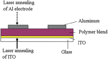
Lasers can be used for the manufacturing of organic solar cells. Reference Kim, Pique, Kushto, Auyeung, Lee, Arnold and Kafafi75–Reference Kim, Kushto, Arnold, Kafafi and Pique77 In Ref. 79, the authors showed that the required thermal annealing step in the fabrication of high efficiency organic solar cells could be achieved using laser annealing process. Thermal annealing is required to optimize the surface morphology to increase efficiency. The laser annealing process avoids the intermixing of different layers and the heating of the substrate can be avoided. Figure 17 shows the schematic of organic solar cell design and application of laser annealing process. Reference Okraku, Gupta and Wright78
Schematic of organic solar cell device showing laser annealing of indium tin oxide (ITO) and aluminum. Reference Okraku, Gupta and Wright78

Laser processing applications for solar thermal and thermophotovoltaics
Solar thermal
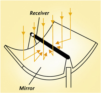
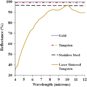
The solar thermal systems generate electric power by absorbing the sunlight to generate heat and then heat is converted into electric power. The key element in solar thermal systems is the solar receiver, which captures the sunlight and transfers the heat energy to flowing fluid, as shown in Fig. 18. 79 The solar receivers are fabricated with a multilayer approach such that solar light is efficiently absorbed but infrared radiation from the heated receiver is minimized to minimize the radiated thermal loss. The authors in Ref. Reference Ungaro, Gray and Gupta81 have demonstrated a high efficiency solar receiver by laser sintering of tungsten nanoparticles on a stainless steel substrate. Through the control of laser processing parameters, the morphology of the sintered nanoparticle layer is governed such that high solar absorptance can be achieved with low thermal emittance. Figure 19 shows the infrared reflectance spectra of laser-sintered layer on stainless steel substrate. The efficiency of solar thermal systems increases with higher operating temperatures as governed by the Carnot cycle limit. So, solar thermal receiver must operate at temperatures higher than 500 °C and preferable greater than 650 °C.
Schematic of solar receiver in a solar thermal system. 79

Measured reflectance for gold, stainless steel, tungsten, and laser-sintered tungsten. Reference Shah and Gupta80

Thermophotovoltaics
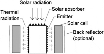
The efficiency of semiconductor solar cells is lowered by the thermalization of high-energy photons (with energies greater than the band gap) and the transmission of low-energy photons (with energies less than the band gap). The solar cell efficiency can be enhanced by absorbing the broad solar spectrum and emitting the radiation into a narrow spectral range to match the band gap of semiconductor solar cell. Thermophotovoltaics are based on this approach and Fig. 20 shows the operation of a thermophotovoltaic system. The concentrated sunlight is absorbed by the receiver and the emitter generates the infrared radiation in a narrow spectral range to match the solar cell band gap. High-power lasers can be used to fabricate solar receivers and emitters. A laser microtextured surface described previously under light trapping structures section can be an efficient solar receiver. The morphology of the emitted surface can be controlled by laser processing to cause the IR emission in a narrow spectral range.
Schematic of thermophotovoltaic system. Reference Ungaro, Gray and Gupta81

Laser processing for thermoelectrics, fuels cells, and other renewable
Energy sources
Electric power is generated in thermoelectrics due to charge carrier flow under the generated temperature gradients. The figure of merit is given by the dimensionless value Reference MacDonald82 :
 $$ZT = {{{S^2}\sigma } \over k}T\quad ,$$
where σ is the electrical conductivity; S is the Seebeck coefficient; k = k e + k L is the thermal conductivity, which contains contributions from electron (k e) and lattice (k L) thermal conduction Reference Nolas, Sharp and Goldsmid83,Reference Kittel84 ; and T is the absolute temperature. The Seebeck coefficient characterizes the thermopower of the material, which describes the voltage developed when a temperature gradient is present. Optimizing ZT is a significant challenge as improving one parameter often adversely affects another. For instance, according to the Wiedemann-Franz law, Reference Franz and Wiedemann85 the electrical and thermal conductivity of metals are proportional to each other, making it difficult to reduce k without also reducing σ.
Recently, it was shown that the thermal conductivity could be strongly reduced through nanostructuring of the material. Reference Bux, Blair, Gogna, Lee, Chen, Dresselhaus, Kaner and Fleurial86 A promising approach involves nanocrystalline materials with grain sizes of a few tens of nanometers, in which enhanced phonon scattering at grain interfaces leads to a strong reduction of the thermal conductivity without negatively affecting the electrical conductivity. Reference Wang, Lee, Lan, Zhu, Joshi, Wang, Yang, Muto, Tang, Klatsky, Song, Dresselhaus, Chen and Ren87–Reference Ma, Hao, Poudel, Lan, Yu, Wang, Chen and Ren91 These “nanograined” materials behave like simultaneous “electron crystals” and “phonon glasses”. Reference Snyder and Toberer92
The nanograined material based films have been prepared by DC hot pressing where grain growth occurs and quantum confinement does not play a role. The pulsed laser sintering method can avoid the grain growth and hence quantum effects could be utilized for the enhancement of thermoelectric power. Reference Stoib, Langmann, Matich, Antesberger, Stein, Angst, Petermann, Schmechel, Schierning, Wolf, Wiggers, Stutzmann and Brandt93
Laser processing can provide manufacturing advantage for fuel cells. Laser drilling and laser sintering are being evaluated for alkaline fuel cell (AFC) applications. 94–Reference Scotti, Trusheim, Kanninen, Naumenko, Shulz-Ruhtenberg, Snitka, Kallio and Franssila96 The AFC converts hydrogen into electric power. Laser-drilled holes perforate the metal substrate for gases to permeate. Currently, over 4000 holes per second can be drilled in thin metal substrates. The laser sintering of powder on a substrate is an alternative method to achieve porous substrate for gas permeability.
Conclusions
Laser processing is very likely to play a greater role in renewable energy applications in the near future due largely to the continuing advances made in improving the power, versatility, and cost effectiveness of laser-processing systems. In particular, processes such as laser doping or firing of localized contacts in silicon solar cells have the potential to produce high-performance solar cells at lower costs. Laser-processing systems for contact formation are more energy efficient than belt furnaces and require relatively small amounts of space. Moreover, the cost of these systems has been steadily decreasing as relatively high-power, low-cost fiber laser systems become readily available for commercial applications.
Large R&D efforts are underway at many organizations around the world developing improved thin film solar cells utilizing materials such as CdTe, CIGS, organic semiconductors, perovskites, etc., and laser-scribing processes are being used to form monolithic thin film modules in most cases.
The throughput of laser processing systems has increased significantly as laser power has increased, high-speed galvo scanning systems have become available and parallel processing via beam splitting has become practical. In modern PV factories, it is desirable for a specific manufacturing tool or system to be able to process silicon solar cells at a rate of about 1 wafer/s. Laser systems under development should be able to process wafers at these speeds for the formation of localized contacts since scientists at Fraunhofer ISE Reference Jager, Oesterlin, Kimmerle and Preu97 have estimated that laser doping of selective emitters could be performed in ~1 s per wafer by using a diffractive optic element to split a laser beam into 70 parallel beams.
It is clear that high-power laser processing of materials is important for renewable energy applications and it has already been accepted for manufacturing of solar cells. New laser-based processes such as laser transfer, laser doping, LFCs, etc. are being developed further for their incorporation into manufacturing processes.
Acknowledgments
M.C. Gupta would like to thank the NSF, I/UCRC program and NASA Langley Professor program for the financial support. We also thank Keye Sun for his help in the preparation of this article.