Introduction
In recent years, antenna structures incorporating metasurfaces (MS) have rapidly gained attention in antenna research due to their unique ability to manipulate and focus electromagnetic waves, as well as their capacity to enhance key properties such as bandwidth, gain, directivity, electromagnetic wave absorption, and electromagnetic cloaking [Reference Shrivastava, Singh, Samantaray, Khan, Gautam and Singh1, Reference Samantaray and Bhattacharyya2]. Researchers have indeed utilized MS to simultaneously enhance gain and improve isolation in multiple-input multiple-output (MIMO) antennas. For wideband applications, the authors [Reference Nkimbeng, Heesu and Ikmo3] proposed an MS-based antenna structure operating in the 3.75–6 GHz band. The antenna structure consists of a 4 × 4 array of unit cells that enhance the gain and a corner-truncated rectangular patch, which is responsible for achieving circular polarization. Similarly, in [Reference Samantaray, Bhattacharyya and Srinivas4], a fractal patch antenna was designed using a partially grounded plane embedded with MS to enhance gain. Consistent with prior research utilizing a single dielectric, the MS structure in this design not only improves gain but also reduces the radar cross-section (RCS). In [Reference Guo, Ding and Vandenbosch5], an MS-based approach is also proposed for broadband RCS reduction in circularly polarized patch antennas. It leverage the principles of destructive interference for RCS reduction and employs the corner truncation method to achieve circular polarization. In [Reference Douhi, Labihi, Eddiai, Lakrit, Achaby and Al-Gburi6], This study demonstrates the strong potential of a PVDF-HFP/BCZT (PVDF-HFP stands for Poly(vinylidene fluoride-co-hexafluoropropylene), while BCZT refers to Barium Calcium Zirconium Titanate) composite as a flexible, high-performance substrate for microwave antennas in wearable technologies. The incorporation of BCZT particles significantly enhanced the composites dielectric properties, thermal stability, and crystallinity, enabling the design of a wideband wearable antenna that performs reliably when integrated into body-worn systems. The use of conductive fabric ensured both user comfort and mechanical flexibility without compromising electrical performance. Furthermore, SAR testing confirmed compliance with international safety standards, reinforcing the antenna’s suitability for practical wearable applications. Similarly in [Reference Douhi, Boumegnane, Chakhchaoui, Eddiai, Cherkaoui and Mazroui7], this study presents a wideband, low-profile, and flexible antenna based on a PMMA-PVDF-HFP-PZT (PMMA-PVDF-HFP-PZT stands for Poly(methyl methacrylate)-Poly(vinylidene fluoride-co-hexafluoropropylene)-Lead zirconate titanate) composite and silver-based ink, tailored for wearable wireless applications. The antenna demonstrates a broad operational bandwidth of 132.16%, a peak gain of 2.76 dBi at 2.92 GHz, and a high radiation efficiency of up to 80% across 1.26–6.17 GHz, making it well-suited for high data rate and reliable communication links. Its performance remains stable under physical deformation, with minimal frequency detuning observed during bending tests. Additionally, SAR values remain within international safety limits, further supporting the antenna’s viability for body-worn use. These findings highlight the antenna’s potential for integration into wearable medical devices, such as contactless doctor badges, enhancing hygiene while enabling efficient, non-invasive communication.
In [Reference Douhi, Eddiai, Idiri, Cherkaoui and Mazroui8–Reference Douhi, Eddiai, Cherkaoui and Mazroui10] antennas are wideband, low-profile, and flexible, integrating metamaterial structures and textile materials for wearable applications. They demonstrate excellent performance across various frequency bands, offering enhanced gain, stable radiation characteristics, and compliance with SAR safety limits, making them ideal for wireless body area networks (WBAN). The incorporation of e-textile conductive materials and a slotted ground plane enhances efficiency and mechanical resilience, ensuring reliable operation even under structural deformations and body loading. These attributes establish the antennas as a promising solution for future wireless and biomedical applications. The significance of this work is to enhance the gain of the antenna, enabling it to capture signals from distant sources. The research demonstrates significant miniaturization compared to previous work, wideband performance, and high radiation efficiency of up to 92.8%. The main challenges in this design include minimizing losses to improve efficiency and addressing stacking difficulties. To overcome these challenges, an MS is placed on a partially grounded plane, which helps reduce losses and eliminates the stacking difficulty associated with positioning the MS at a precise height above the antenna to enhance gain.
In this work, we present the design of a compact, high-gain, LHCP antenna inspired by a metasurface. The antenna consists of a circular patch with a radius of 6.5 mm and a partial ground plane. A  $4 \times 4$ array of unit cells, exhibiting negative permittivity within the frequency range of 7–13.5 GHz, is employed. This array qualifies as a double-negative (DNG) metamaterial, as both its permittivity and permeability are negative within the same frequency range. The DNG metamaterial is strategically placed on the partial ground plane of the microstrip antenna to enhance gain while significantly reducing the overall antenna size, which measures 27 mm × 27 mm × 1.6 mm. The design procedure and key antenna parameters are discussed in detail, step by step, in the following sections.
Design of the antenna prototype
The proposed antenna structure consists of a radiating patch, a partially grounded plane, and an MS is composed of a 4 × 4 array of unit cells. The design process begins with an in-depth analysis of a single unit cell, focusing on its key properties, such as permeability, permittivity, refractive index, and impedance. Notably, the results reveal a negative refractive index within the frequency range of 7–13.5 GHz. This frequency band is targeted for the antenna’s operational bandwidth because, within this range, the unit cell exhibits metamaterial-like behaviour. By strategically placing the metasurface behind the antenna, the back-radiated power is redirected forward, resulting in constructive interference that enhances radiation. This effect results in a significant gain improvement. The design of the unit cell and the microstrip antenna are discussed in the following subsections.
Design of unit cell
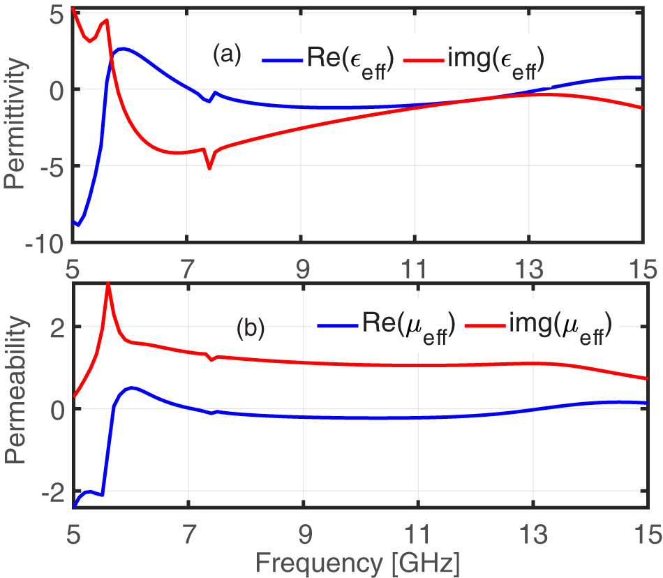
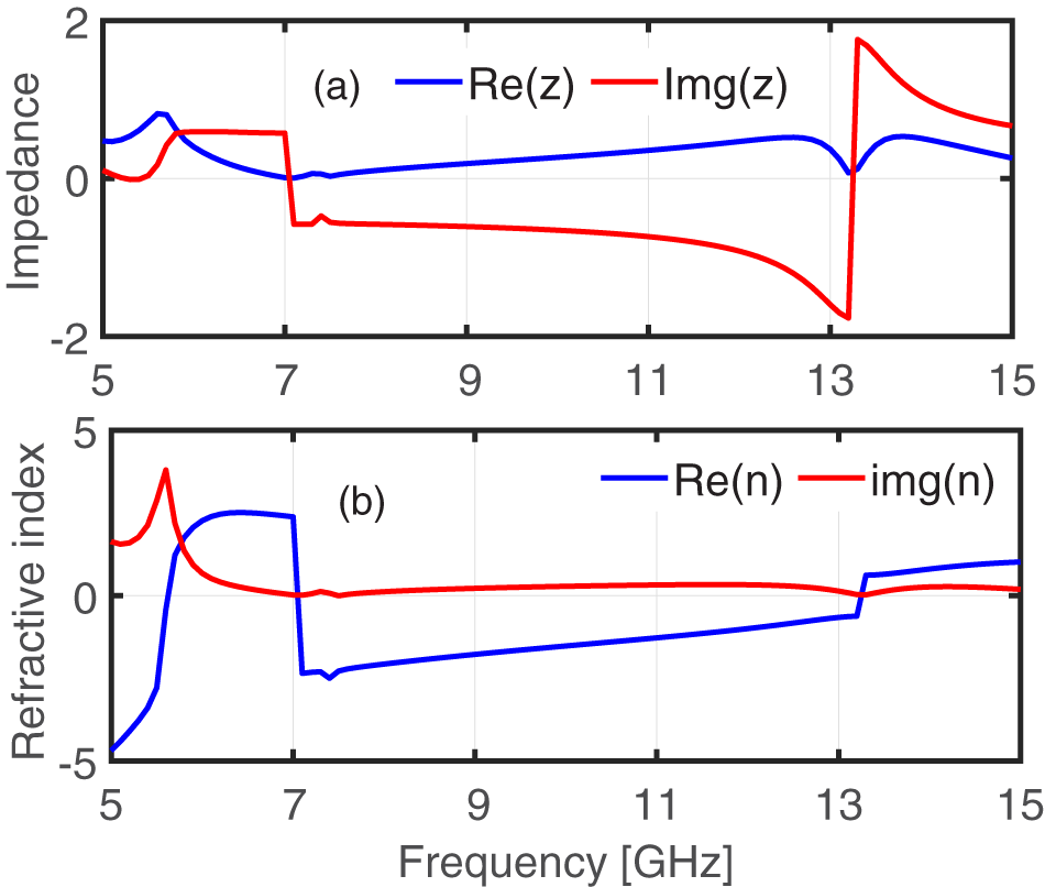
The top and bottom views of the unit cell structure are shown in Fig. 1(a) and (b), respectively. The unit cell has overall dimensions of 6 mm × 6 mm × 1.6 mm and is etched on an FR4 substrate with a permittivity of 4.4 and a loss tangent of 0.02. The design includes a slotted circular annular ring that encloses a concentric circular element. The scattering parameters for this configuration (|S 11| and |S 11|) are computed using HFSS software, which employs a Floquet port to excite the unit cell. These values are then substituted into equations (1)–(4) [Reference Smith, Vier, Koschny and Soukoulis11] to determine the critical parameters of the proposed structure, such as effective permittivity, permeability, impedance, and refractive index. The calculations are performed using a MATLAB code [Reference Numan and Sharawi12], and the results are shown in Figs. 2 and 3 for a single unit cell. Fig. 2 illustrates the real and imaginary parts of the effective permittivity and permeability. While Fig. 3 presents the real and imaginary parts of the effective impedance and refractive index. The real parts of the effective permittivity and permeability are negative over the frequency range of 7–13.5 GHz, identifying the unit cell as a double-negative (DNG) metamaterial. The negative permittivity and permeability also lead to a negative refractive index over this frequency band, making the structure suitable for metasurface applications. The electric field distribution of the unit cell structure is shown in Fig. 4(a). It is observed that the electric field reaches its maximum on the right and left sides of the unit cell, while it is minimal on the top side and within the inner circular element. As a result, the high electric field around the annular ring facilitates coupling between adjacent unit cells, as denoted by Cc [Reference Samantaray and Bhattacharyya13] and illustrated in Fig. 4(b). This coupling primarily arises from the time-varying electric field across the annular ring, which induces a time-varying magnetic field. This magnetic field excites the adjacent unit cell, resulting in a time-varying current. The capacitance between the annular ring and the circular element is minimal compared to the capacitance resulting from the slot cut in the annular ring. This is denoted by Ceq, while the inductance due to the current flow in the annular ring is represented as Leq [Reference Baena, Bonache, Martin, Sillero, Falcone, Lopetegi, Laso, Garcia-Garcia, Gil, Portillo and Sorolla14]. In addition to this, the resistive component has been ignored in Fig. 4(c). Thus, the equivalent circuit diagram for the unit cell structure is formed by combining the inductance and capacitance components, as illustrated in Fig. 4(c). The resonant frequency of this structure is given by: f 0=  $\dfrac{1} {2\pi \sqrt{L_{eq} C_{eq}}}$. Furthermore, when the unit cell is used in an array configuration, as shown in Fig. 4(d), the equivalent circuit includes Cx and Cy, which represent the coupling capacitances between the unit cell and its adjacent unit cells along the x- and y-directions of the centred unit cell, respectively. The details of the antenna design and its corresponding parameters have been discussed in the following sections.
Design of unit cell and its parameters. (a) Top view, (b) bottom view, (c)  $|S_{11}|$ and
 $|S_{21}|$ of unit cell, and (d) simulation of unit cell applying Floquet Port by using HFSS. [R 1 = 1.1 mm, R 2 = 2.43 mm, R 3 = 1.75 mm, L 1 = 0.68 mm, L 2 = 0.5 mm, L 3 = 3 mm.]

Unit cell’s real and imaginary part of (a) effective permittivity and (b) effective permeability.

Unit cell’s real and imaginary part of (a) effective impedance and (b) effective refractive index.

Unit cell’s (a) electric field distribution, (b) coupling between adjacent unit cells, (c) equivalent circuit model, (d) MS and (e) equivalent circuit of MS [2].

 \begin{align}
z&= \sqrt{\dfrac{(1+S_{11})^{2} -{S_{21}}^{2}} {(1-S_{11})^{2} -{S_{21} }^{2}} }
\end{align}
 \begin{align}
n &= \frac{1}{kd} {\cos^{-1} \left(\frac{1}{2 S_{21}}\right) \left(1-{S_{11}}^{2}+{S_{21}}^{2}\right)}
\end{align}
 \begin{align}
\mu_{eff} &= n\times z
\end{align}
 \begin{align}
\epsilon_{eff} &= \frac{n}{z}
\end{align}
Where, ϵeff = effective permittivity, µeff = effective permeability,  $z =$ effective impedance, and
 $n =$ effective refractive index of unit cell.
 \begin{align}
Z_{1}&= j\omega L_{1}+ \frac{1}{j\omega C_{1}}
\end{align}
 \begin{align}
Z_{2}&= \frac{1}{R_{1}}+j{\omega}C_{2}+\frac{1}{j\omega L_{2}}\nonumber\\
&= \frac{j\omega L_{2} + j\omega C_{2}(j\omega L_{2} R_{1})+ R_{1}} {j\omega R_{1} L_{2}}
\end{align}
 \begin{align}
Z_{3}&= \frac{1}{j\omega C_{3}}
\end{align}
 \begin{align}
Z_{4}&= \frac{1}{R_{2}}+j\omega C_{4} +\frac{1}{j\omega L_{3}}\nonumber\\
&= \frac{j\omega L_{3} +j\omega C_{4}(j \omega L_{3} R_{2})+ R_{2}} {j \omega R_{2}L_{3}}
\end{align}
 \begin{align}
{Z_{5}}&= \frac{1}{j\omega C_{3}}
\end{align}
 \begin{align}
Z_{in}&= Z_{1} +Z_{2} + Z_{3} + Z_{4} + Z_{5}
\end{align}
Design of the radiating patch with MS
Fig. 5 illustrates the step-by-step design process of the proposed antenna. In Fig. 5(a)–(i), a circular patch is connected to a microstrip feed line, with a partial ground plane placed on the bottom side of the antenna. In Fig. 5(a)(ii), the ground plane remains the same as in Fig. 5(a) – (i), but a stub is added just above the feed point on the top side. In Fig. 5(a)(iii), the top side remains unchanged from the previous structure, but the ground plane is loaded with MS. The S 11 responses of structures used in Fig. 5(a) are shown in Fig. 5(b) by the green, blue, and red traces, respectively. Although the variation in bandwidth between Fig. 5(b)(i) and Fig. 5(b)(ii) is not significant, the depth of the S 11 response in Fig. 5(b)(iii) is noticeably improved compared to the structure in Fig. 5(b)(ii). Therefore, the final structure chosen is Fig. 5(iii).
(a) Step by step design of proposed antenna (i) without stub on the front side and MS on bottom side, (ii) with stub on front side and without MS on the bottom side, and (iii) With stub on front side and MS on bottom side and (b) S11 parameters for (a).

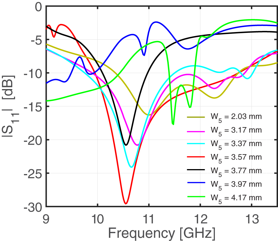
The radiating patch of the antenna consists of a circular element with a radius of 6.5 mm, coupled to a microstrip feed line measuring 11.18 mm × 3 mm. The opposite side of the radiating element features an array of unit cells and a partially grounded plane of dimensions 27 mm × 1 mm. A horizontal stub, with dimensions of 2.5 mm × 10 mm, is placed 2.5 mm above the bottom part of the antenna. The complete antenna structure has sizes of 27 mm × 27 mm × 1.6 mm, and its dimensions are illustrated in Fig. 6, which utilizes FR4 dielectric material. As the unit cell array expands from 1 × 1 to 4 × 4, the antenna gain increases. This is because, when we gradually increase the number of unit cells from a 1 × 1 to 4 × 4 array on the MS, the convergence of the incident electromagnetic (EM) wave in a particular direction also increases. Therefore, we select the MS with a 4 × 4 array of unit cells. However, a 5 × 5 array cannot be used due to space constraints. Fig. 7 depicts the variation of the gap between the ground plane and the lower row of MS (W 5). As W 5 increases from 2.03 mm to 3.57 mm, the depth of the resonance frequency increases and shifts from right to left. The bandwidth also increases with W 5, reaching its maximum at W 5=3.57 mm. Beyond this value, the bandwidth decreases drastically from W 5 = 3.57 mm to W 5=4.17 mm. Therefore, the optimal value of W 5 is chosen as 3.57 mm, as it provides the maximum bandwidth and resonance depth. In the next section, we discuss the simulated and measured parameters of the proposed prototype.
Designed antenna prototype with proper dimensions (a) top view, (b) bottom view, (c) fabricated top view, and (d) fabricated bottom view. [R = 6.5 mm, W 1 = 27 mm, W 2 =11.18 mm, W 3 = 2.5 mm, W 4 = 6 mm, W 5 = 3.57 mm, L 1 = 10 mm, L 2 = 27 mm, L 3 = 2.1 mm, L 4 = 6 mm, width of ground plane = 1 mm.]

Response of S 11 of proposed antenna when varying W 5.

Discussion of results
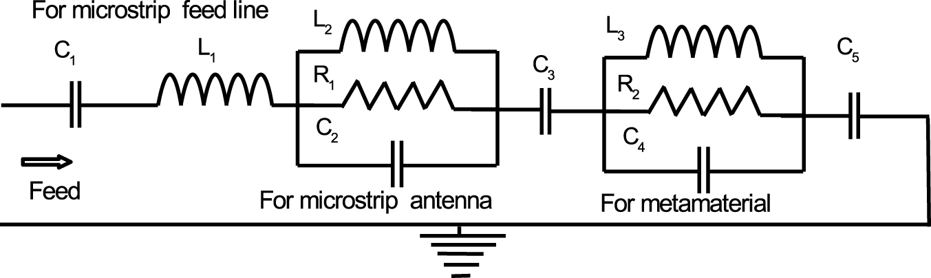
The MS-inspired antenna has been fabricated using the photo etching method, and its parameters have been tested in an anechoic chamber with the KEYSIGHT N5224B PNA Microwave Network Analyzer. Fig. 8 depicts the image of the Network Analyzer while measuring the S11 parameter of the proposed antenna. The designed prototype operates in two frequency bands: one from 7 to 7.6 GHz and another from 9.7 to 13 GHz. The first band is not shown in any figures in this paper because, in this region, the prototype exhibits low gain, and our primary objective is to enhance gain in the X-band frequency range. The simulation of the antenna prototype has been performed using High Frequency Structure Simulator (HFSS) software, whereas the equivalent circuit diagram of the designed prototype, modelled using Advanced Design System (ADS) software through an iterative method, is shown in Fig. 9. Modelling an antenna prototype using an equivalent circuit provides a simplified yet effective way to analyze and optimize its performance. This approach translates the complex electromagnetic behavior of an antenna into familiar circuit elements such as resistors, inductors, and capacitors. The circuit model helps engineers understand the impedance characteristics of the antenna without requiring full-wave electromagnetic simulations. It offers an intuitive way to analyze key antenna parameters, including resonance, bandwidth, and impedance matching. Full-wave electromagnetic simulations (e.g., using HFSS or CST) can be computationally expensive and time-consuming. In contrast, circuit models provide a faster alternative for preliminary analysis, significantly reducing computational costs in the early design stages. The feed line with stub structures is represented as a series combination of L 1 and C 1. The equivalent circuit for the patch includes the first tank circuit, comprising L 2, C 2 and R 1, followed by C 3, which represents the capacitance between the patch and the MS. The second tank circuit represents the MS, where C 4 accounts for Cx, Cy, and Ceq. Finally, the gap W 5 between the partial ground plane and the lower array of the MS introduces C 5, as shown in Fig. 9.
Measured S 11 parameter of proposed antenna.

Equivalent circuit of proposed antenna. [L 1 = 599.74pH, L 2 = 382.94pH, L 3 = 100.03pH, C 1 = 2.47pF, C 2 = 614.20fF, C 3 = 36.4 pF, C 4 = 2.63 pF, C 5 = 9.21 pF, R 1 = 40 Ohm, R 2 = 59.99 Ohm.]

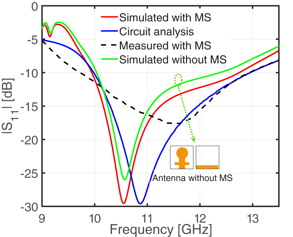
Fig. 10 compares the simulated, measured, and equivalent circuit responses of the S 11 parameter for the designed prototype. The measured bandwidth is 3.3 GHz (from 9.7 to 13 GHz), while the simulated bandwidth is 2.75 GHz (from 10 to 12.75 GHz), and the bandwidth from circuit analysis is 3 GHz (from 10 to 13 GHz). Additionally, the maximum S 11 dips for the measured, simulated, and circuit analysis results are −18, −29, and −29 dB, occurring at 11.5, 10.5, and 10.85 GHz, respectively. Comparing the S 11 parameter of the proposed antenna with that of the antenna without MS reveals that the bandwidth of the antenna without MS is narrower by 0.35 GHz ((10–12.75 GHz)–(10–12.4 GHz)) compared to the antenna with MS. Furthermore, the depth of S 11 is also smaller for the antenna without MS. All the relevant results of the proposed antenna are shown in Table 1. The proposed antenna has been designed using the FR4 dielectric material. The difference between the simulated and measured results may occur due to fabrication tolerances. This could be attributed to soldering between the microstrip feed line and the SMA connector or copper loss in the metallic portion of the designed antenna prototype above and below the FR4 dielectric material during polishing. Additionally, the shift may be caused by the insertion loss of the SMA connector, leading to discrepancies between the frequency responses in the simulated and measured results as shown in Fig. 10.
Simulated and measured S-parameters and circuit responses of the designed antenna.

Some important parameters of the proposed antenna

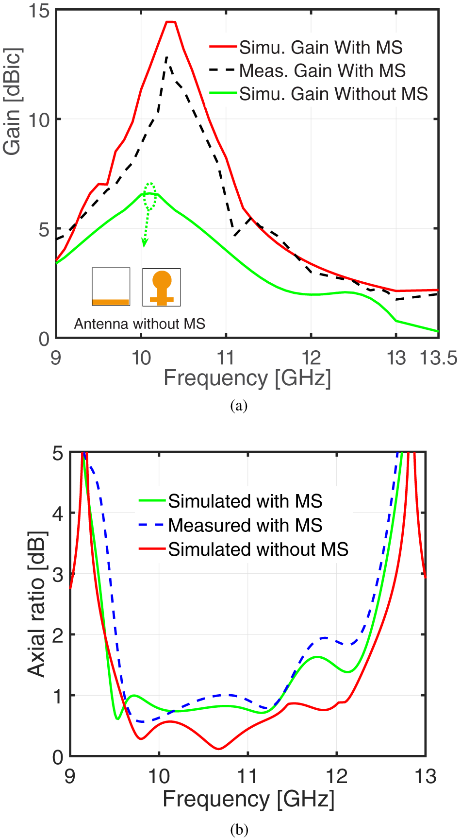
Fig. 11(a) shows the measured and simulated gains of the prototype antenna, compared with those of a conventional antenna (an antenna without MS). The maximum measured gain of the designed prototype is 12.8 dBic at 10.3 GHz, while the simulated gain reaches 14.4 dBic at the same frequency. In contrast, the maximum gain of the conventional antenna is 6.6 dBic at 10.1 GHz. The measured gain increases significantly from 10 to 11 GHz, after which it drops to 2.2 dBic at 13 GHz. Similarly, the simulated and measured axial ratio bandwidths of the prototype antenna with MS are 9.45–12.52 and 9.3–12.47 GHz, respectively, whereas the simulated result for the prototype antenna without MS is found to be 9.4–12.7 GHz, as illustrated in Fig. 11(b). Notably, the simulated and measured 3 dB axial ratio bandwidths are nearly identical. The circular polarization of the proposed antenna is solely due to the circular patch, not the MS. Fig. 12 depicts the surface current distribution on the radiating element and MS at various frequencies, including 10, 11, 12, and 13 GHz. At 13 GHz, the maximum current density (CD) is observed at the top-left section of the circular patch and on the ground plane. In contrast, at 12 GHz, the highest CD occurs on either side of the lower part of the microstrip feed line. The current density on the MS structure decreases sequentially at frequencies of 13, 10, 12, and 11 GHz. Fig. 13 shows the laboratory set-up used for measuring the antenna’s radiation pattern and scattering parameters. The Antenna Under Test (AUT) is positioned in front of a calibrated reference horn antenna with known gain, at a minimum distance of  $d = \frac{2D^2}{\lambda}$ inside an anechoic chamber. Here, D denotes the largest dimension of the AUT, d is the separation between the AUT and the reference antenna, and λ is the operating wavelength. To measure the YZ-plane radiation pattern, the AUT is fixed at
 $\phi = 0^\circ$ and rotated from
 $\theta = 0^\circ$ to 180∘ (vertical scan), as shown in the upper left and lower right parts of Fig. 13. For the XY-plane radiation pattern, the AUT is fixed at
 $\theta = 90^\circ$ (horizontal scan) and rotated from
 $\phi = 0^\circ$ to 360∘, as depicted in the upper right and lower left sections of Fig. 13.
(a) Gain of the designed antenna and (b) axial ratio of proposed antenna.

Surface current density of proposed prototype at (a) 10 GHz, (b) 11 GHz, (c) 12 GHz, and (d) 13 GHz.

Pictures of the set-up while measuring the parameters of a designed antenna in the lab.

Fig. 14 presents the normalized 2D field patterns of the intended prototype at frequencies of 10.4 and 12 GHz. The red and blue colour traces represent the left-handed circular polarization (LHCP) and right-handed circular polarization (RHCP) radiation patterns, respectively. In both the XZ- and YZ-planes, LHCP dominates, except at angles θ = 60∘, and 210∘ in the XY-plane at 10.4 GHz, and at θ = 60∘ and 270∘ in the same plane at 12 GHz.
Two-dimensional radiation parameters of designed antenna at (a) 10.4 GHz and (b) 12 GHz.

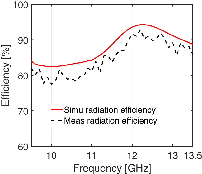
Fig. 15 shows the vector current density (VCD) at a frequency of 11.4 GHz at t = 0, T/4, 2T/4, and 3T/4. The resultant VCD at t=0 is almost horizontal toward the right-hand side, as shown in Fig. 15(a). Similarly, for t = T/4, 2T/4, and 3T/4, the resultant VCD points vertically downward, toward the left-hand side, and vertically upward, respectively, as shown in Fig. 15(b)–(d). Thus, the resultant VCD rotates according to the left-hand rule. This type of rotation in the VCD confirms that the polarization is Left-Handed Circular Polarization (LHCP). Two main types of parameters are presented: simulated and measured in the lab. Notably, some tolerable differences exist between the simulated and measured values of the antenna parameters, largely due to ambient effects, faulty soldering, and other fabrication-related imperfections. Fig. 16 shows the radiation efficiency of the proposed antenna. From same figure, we observe that the maximum simulated efficiency is 94.2%, whereas the maximum measured efficiency is 92.8%, recorded at 12.3 and 12.2 GHz, respectively.
Vector current density (VCD) at a frequency of 11.4 GHz for different times.

Simulated and measured radiation efficiency values of the proposed antenna.

Table 2 compares the present work with several recent studies from the literature, spanning references [Reference Baena, Bonache, Martin, Sillero, Falcone, Lopetegi, Laso, Garcia-Garcia, Gil, Portillo and Sorolla14–Reference Wu, Ji, Li, Liu, Zhang, Zhang and Kong20]. As noted in references [Reference Baena, Bonache, Martin, Sillero, Falcone, Lopetegi, Laso, Garcia-Garcia, Gil, Portillo and Sorolla14–Reference Baba, Hashmi, Esselle, Marin and Jan17], all the high-gain antennas discussed are linearly polarized (LP). Among these, the antenna with the smallest profile size (1.16λ 0) achieves a moderate gain of 9.3 dBi [Reference Baena, Bonache, Martin, Sillero, Falcone, Lopetegi, Laso, Garcia-Garcia, Gil, Portillo and Sorolla14], while the antenna with the highest gain (18.8 dBi) has the largest profile size, measuring 3.1λ 0 [Reference Sharma, Gangwar, Kanaujia, Dwari and Kumar16]. Among the circularly polarized (CP) antennas [Reference Ameen and Chaudhary18–Reference Wu, Ji, Li, Liu, Zhang, Zhang and Kong20], the antenna in [Reference Ameen and Chaudhary18] has the smallest size (0.27λ 0) and the lowest gain of 4.74 dBic, while [Reference Wu, Ji, Li, Liu, Zhang, Zhang and Kong20] reports the maximum gain of 13 dBic, with the largest profile size measuring 1.4λ 0. In comparison, the proposed high-gain LHCP antenna achieves a maximum gain of 12.8 dBic and has a moderate size of 0.88λ 0. Among all the papers mentioned in Table 2, apart from our design, the antenna described in [Reference Wu, Ji, Li, Liu, Zhang, Zhang and Kong20] stands out as the best because, offering CP, a high gain of up to 13 dBic, and a moderate size of 1.4λ. However, when comparing our designed antenna with [Reference Wu, Ji, Li, Liu, Zhang, Zhang and Kong20], it is observed that the gain is slightly lower by 0.2 dBic, while the dimensions are significantly smaller (37% less) than those in [Reference Wu, Ji, Li, Liu, Zhang, Zhang and Kong20]. Therefore, it is concluded that our proposed antenna is superior to all the antennas listed in Table 2.
Comparative study of the proposed antenna with some other high-gain antennas

Conclusion
A LHCP, double-negative metamaterial-inspired (DNG-MS), miniaturized microstrip antenna has been developed to enhance gain performance. The antenna achieves an impedance bandwidth of 3.3 GHz (9.7–13 GHz) and a 3 dB axial ratio bandwidth of 3.02 GHz (9.45–12.47 GHz). The VDC pattern confirms that the antenna exhibits left-handed circular polarization (LHCP). By integrating the MS structure on a partial ground plane, the gain significantly increases from 6.6 dBic, achieved by a conventional antenna, to 12.8 dBic. By observing Table 2, it can be concluded that achieving such high gain in a miniaturized LHCP antenna is the key novelty of our design. The prototype antenna operates within the upper X-band and lower Ku-band, making it highly suitable for marine applications. To further advance this work, future studies may explore the integration of tunable or reconfigurable metamaterials to achieve dynamic gain control and beam-steering capabilities. Additionally, implementing multilayer metamaterial superstrates with varying unit cell geometries could lead to further enhancement in gain performance.
Competing interests
The author(s) declare none.

Manoj Kumar Shrivastava was born in East Champaran, Bihar, India, in 1974. He received his B. Tech. degree in Electronics Engineering from the Institute of Engineering, Pulchowk Campus, affiliated with Tribhuvan University, Nepal, in 2002. He later earned his master’s degree in Electronics Engineering from IIT (BHU), Varanasi, India, in 2012. Currently, he is pursuing a Ph.D. at the Indian Institute of Information Technology (IIIT) Guwahati, India. His research interests include ultra-wideband (UWB) antennas, circularly polarized metamaterial-based antennas, and cloaking using metamaterials.

Ripudaman Singh received the B.E. degree (Hons.) in electronics and communication engineering from the University of Rajasthan, Jaipur, India, in 2009, and the M.Tech. and Ph.D. degrees in electronics and electrical engineering from the Indian Institute of Technology Guwahati, Guwahati, India, in 2012 and 2018, respectively. He is currently an Assistant Professor with the Department of Electronics and Communication Engineering, Indian Institute of Information Technology Guwahati. From May 2020 to December 2020, he was a Postdoctoral Fellow with the Electrical and Computer Engineering Department, National University of Singapore, Singapore. His research interests include wireless sensor networks, distributed algorithms, antenna design and performance modelling of communication systems.

Diptiranjan Samantaray received the B.Tech. degree in Electronics and Telecommunication Engineering from the Biju Patnaik University of Technology, Rourkela, India, in 2009, the M.Tech. Degree in Electronics and Communication Engineering from the Indian Institute of Technology, Kharagpur, India, in 2015, and the Ph.D. degree in Microwave Engineering from the Indian Institute of Technology (Banaras Hindu University), Varanasi, India, in 2022. Currently, he is working as an assistant professor in the Department of Electronics and Communication Engineering, Faculty of Technology, University of Delhi. His areas of interest lie in electromagnetic, antennas, and metamaterials. In his teaching and research experience, he has authored or co-authored many technical papers in international journals and conference proceedings. Dr. Samantaray served as the founding treasurer of the IEEE Photonics Society Student Branch Chapter and the chairperson of the IEEE MTT-S Student Branch Chapter, IIT (BHU), Varanasi, India.

Anil Kumar Gautam received the B.E. degree in electronics and communication engineering from the BT Kumaon Institute of Technology, Almora, India, in 1999, and the Ph.D. degree in electronic engineering from Indian Institute of Technology (BHU) Varanasi, India, in 2007. In 2000, he joined the Department of Electronics and Communication Engineering, G B Pant Institute of Engineer- ing and Technology, Pauri Garhwal, India, as an Assistant Professor and appointed as Associate Professor in 2009. He has also worked as Professor and Dean at School of Information and Communication Technology, Gautam Buddha University, Greater Noida, India from 2016 to 2018. He is currently working as Professor at Department of Electronics and Communication Engineering, G B Pant Institute of Engineering and Technology, Pauri Garhwal, India. Dr Gautam is a Senior member of IEEE. He has delivered many expert talks in FDP, workshops and STCs. He has supervised his 33 M. Tech and 08 Ph.D. theses and currently supervising his one Ph.D. theses in microstrip antenna. He has authored or co-authored more than 125 SCI research papers published in the refereed international journals, such as the IEEE Transactions on Antenna and Propagation, IEEE Antenna and Wave Propagation Letters, Microwave and Optical Technology Letters, Springer, and so on. He has authored 13 books in electronics engineering with a focus on digital electronics, antenna, and microwave engineering. His current research interests include design and modelling of active microstrip antenna, microstrip antennas with defected Ground structure, ultrawide bandwidth antennas, and reconfigurable antennas, reconfiguration Antenna array, and circular polarized antenna. Dr Gautam has also served as Dean (Academic), Dean of school of ICT, Head of the Department, Registrar G B Pant Institute of Engineering and Technology, Pauri Garhwal, India in 2016. He was a Chairman of the Board of Study, School of Information and Communication Technology, and a member of the Board of Management and Academic Council, Gautam Buddha University. He is also an Active Member of the Board of Study, Academic Council, and many other academic committees of GBPEC, Pauri Garhwal. He is also a member of the BOS, Hemwati Nandan Bahuguna Garhwal University, Srinagar, India, and Uttarakhand Technical Uni- versity, Dehradun, India. He was a Nodal Officer, TSP and SCSP Grants by the Government of Uttarakhand and executed several projects under these grants. He is a member of Editorial Board of the International Journal of RF and Microwave Computer-Aided Engineering. He is also in reviewers’ panel for the IEEE Transactions on Antenna and Propagation, IEEE Antenna and Wave Propagation Letters, IET Microwaves, Antennas and Propagation, Wireless Personal Communications (Springer), the International Journal of Electronics, the International Journal of Microwave and Wireless Technologies, the International Journal of Antenna and Propagation, and so on. He is a Senior Member of IEEE and member various other technical societies also. He is also recipient Education Leadership Awards 2018, awarded by Dewang Mehta National Education Awards, India. His paper entitled “Tapered Fed Compact UWB MIMO-Diversity Antenna with Dual Band-Notched characteristics has been awarded First prize of ‘Governor’s Award 2019 for best Research Paper by Governor, State of Uttarakhand.

Amit Kumar Singh received the Ph.D. degree from IIT (BHU), Varanasi, in 2010. He has been working as an Associate Professor with the Electronics Engineering Department, IIT (BHU), since 2012. He has published and co-authored over 70 journal articles and conference papers. His research interests include the areas of design of millimetre frequency antennas, feeds for parabolic reflectors, dielectric resonator antennas, microstrip antennas, EBG, artificial magnetic conductors, soft and hard surfaces, antennas for RFIDs, phased array antennas, and computer-aided design for antennas.