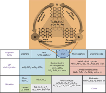
Nanomaterials provide an excellent sensing platform for various bio-sensors because they can be easily fabricated, chemically modified, and can be integrated into microfluidic chips or point-of-care devices. Reference Yang, Asiri, Tang, Du and Lin1,Reference Pumera2 Here a brief account of two-dimensional (2D) nanomaterials (various types of 2D materials are shown in Fig. 1) platform with graphene as the “prime-material” and protein-as the basic biomolecule is discussed to understand the importance of bio–nano interfaces in various applications including biosensors, electronics, and drug carriers. We conclude with a brief overview of beyond-graphene 2D materials, in the form of atomically-thin molybdenum disulfide (MoS2) as an attractive platform for next-generation label-free biosensors.
A spectrum of 2D materials is shown. The class of boron–carbon–nitrogen is expanded in the inset, showing the possibilities of engineering the band gap of graphene by similarly sized heteroatom doping. Reference Ci, Song, Jin, Jariwala, Wu, Li, Srivastava, Wang, Storr, Balicas, Liu and Ajayan3,Reference Geim and Grigorieva4 Reproduced with permission from Nature Publishing Group. Reference Geim and Grigorieva4

Graphene, a 2D material with exotic physico-chemical properties such as ultra-thinness (∼0.5 nm), high surface area (2630 m2/g), enormous carrier mobility (200,000 cm2/V s), good electrical conductivity (∼107 S/m), large mechanical strength, high thermal, and chemical stability, has attracted researchers in all fields due to the amenabilities in tuning its properties for various applications. Reference Georgakilas, Otyepka, Bourlinos, Chandra, Kim, Christian Kemp, Hobza, Zboril and Kim5 Above all, the electronic properties of graphene are highly sensitive to the changes in its environment. Reference Qiyuan, Shixin, Zongyou and Zhang6 Control over the electronic and electro–chemical properties of graphene by doping or by controlling defects has opened a new avenue for graphene based electronic and electrochemical sensors. Reference Vineesh, Alwarappam and Narayanan7 Controllability in the electronic properties by size and shape confinement effects also leads to interesting optical properties, and these have been used in various fields including multimodality imaging. Reference Kundu, Yadav, Shelke, Narayanan, Vajtai, Ajayan and Pillai8
Ease of functionalization of graphene brings the opportunity to bind bio-molecules to graphene surface via covalent and noncovalent bonding. Reference Georgakilas, Otyepka, Bourlinos, Chandra, Kim, Christian Kemp, Hobza, Zboril and Kim5 This property of graphene along with others has been utilized in controlled drug delivery, Reference Yang, Zhang, Ma, Huang, Wang and Chen9–Reference Li, Huang, Liu, Wang, Song, Zhou and Zhang11 targeted imaging, Reference Cong, He, Lu and Yu12,Reference Miao, Tongay, Petterson, Berke, Rinzler, Appleton and Hebard13 biosensors, Reference Chen, Tang and Li14,Reference Min, Kim, Cho and Kim15 immunosensors, Reference Loo, Bonanni, Ambrosi, Poh and Pumera16–Reference Hou, Cui, Xu, Gao, Huang and Tang18 etc. The capability of graphene to adsorb biomolecules via π–π stacking or electrostatic interaction opened the possibility for making various sensors. But, for the successful use of these bio–nano interfaces in bio–nanotechnology, understanding the interface interactions is highly demanding. For example, understanding the bonding between the basic biomolecule–protein and graphene will play significant role in many fields such as biocompatible hybrid materials, nanomedicine, biomimetic sensors and protein separation and purification strategies. Reference Nair, Wu, Jayaram, Grigorieva and Geim19 Moreover, studying the interactions of graphene and protein in different environments such as water, will also help to unravel the interface phenomena. These investigations may extend from colloidal scale to molecular level. Reference Zboril, Karlicky, Bourlinos, Athanasios, Steriotis, Stubos, Georgakilas, Safarova, Jancik, Trapalis and Otyepka20–Reference Zhang, Zhou, Xie, Zeng, Zhang and Peng22
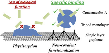
Single layer graphene with its mechanical flexibility, transparency, conductivity, and outstanding surface area offers its applicability in lab-on-a-chip analysis systems, Reference Crevillen, Avila, Pumera, Gonzalez and Escarpa23,Reference Crevillen, Pumera, Gonzales and Escarpa24 field effect transistor (FET) integrated microfluidic systems Reference Sudibya, He, Zhang and Chen25,Reference He, Sudibya, Yin, Wu, Li, Boey, Huang, Chen and Zhang26 for point-of-care devices, wireless biosensors, etc. Biomacromolecules such as proteins were also interfaced with graphene, Reference Chen, Tang and Li14,Reference Yi, Park, Singh, Lee, Kim and Kim27 but the number of reports on the functionality of proteins after functionalization is limited. Reference Lee, Joung, Kim and Park28,Reference Kodali, Scrimgeour, Kim, Hankinson, Carrol, Heer, Berger and Curtis29 This is due to the fact that graphene interacts with the hydrophobic components of biomolecules and alter their conformation and disrupt the biological activities. These structural changes can completely denature the protein upon adsorption on graphene surface, and hence graphene–biomolecules interface should be considered seriously. Loss of biological function of a protein by the loss of specific binding is demonstrated in Fig. 2.
The loss of specific function of Concanavalin A protein by a nonspecific binding with single layer graphene and its functioning after a specific binding. Reproduced with permission from American Chemical Society. Reference Alava, Jason Mann, Théodore, Benitez, William, Parpia and Craighead30

The structure distortion of an adsorbed protein may depend on various factors—orientation of graphene, number of layers and energetics of the equilibrium between folded and denatured states. Reference Haynes and Norde31,Reference Roach, Farrar and Perry32 A few studies have been reported on these aspects of protein–graphene interfaces, and the study using a quartz crystal micro balance to characterize the immobilization of a protein on single layer graphene, Reference Alava, Jason Mann, Théodore, Benitez, William, Parpia and Craighead30 cryo-transmission electron microscope based studies to look in to the graphene–protein interface and small angle neutron scattering studies Reference Green and Hersam33,Reference Gurusaran, Rai, Qian, Weiss, Urban, Li, Ma, Narayanan, Ajayan, Sekar, Viswanathan and Renugopalakrishanan34 are name a few.
Recent studies indicate that water will play a crucial role in the assembly of proteins on a solid substrate by regulating the interactions between binding partners and conformations of proteins. Reference Thirumalai, Reddy and Straub35 Graphene–protein assembly will be affected by the noncovalent interactions and heterogeneous and dynamic hydration environments. Reference Zhang, Wu, Guo and Zhang36 Hence, understanding the interactions between graphene, protein, and water play a key role in bio–nano interfaces. But, the properties and structure of water regulated graphene–protein interfaces are not well characterized or explored till to date.
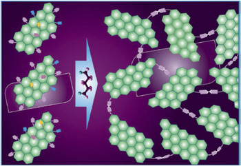
One of the possibilities for exploring the graphene–protein interfaces experimentally is by creating nonplanar interfaces. This can be achieved by making different geometries of single layer graphene. One of the hot topics of present graphene research is on the development of 3-dimensional (3D) (an example is shown in Fig. 3) graphene monoliths for various applications. Reference Georgakilas, Otyepka, Bourlinos, Chandra, Kim, Christian Kemp, Hobza, Zboril and Kim5 The applications of these 3D monoliths may extend from microelectronic, biosensors to energy devices. Reference Hashim, Narayanan, Romo-Herrera, Cullen, Hahm, Lezzi, R Suttle, Kelkhoff, Munoz-Sandoval, Ganguli, Roy, Smith, Vajtai, Sumpter, Meunier, Terrones, Terrones and Ajayan37–Reference Wang, Sun, Routh, Kim, Huangb and Chen40
Schematic of a 3D graphene network developed from single layer graphene. Reference Vineesh, Alwarappam and Narayanan7

Such a 3D morphology may help the interface studies by using a microscopic approach. The 3D structure will also provide the high surface area as in the case of single layer graphene. Efficient bio-sensing has been reported using a 3D graphene nano ribbon (GNR) electrodes and the efficiency of 3D electrodes were compared with 2D electrodes. Reference Vineesh, Alwarappam and Narayanan7 Better and efficient sensing of bio-analytes such as dopamine and ascorbic acid were observed from these modified electrodes. An electrochemical sensing platform was used for checking the efficacy of these electrodes. These studies reveal that high surface area of the electrodes provides a linear diffusion assisted detection mechanism for bio-analytes. The conjugation of proteins into these 3D graphene electrodes, and studies on their interfaces and orientation are not yet explored.
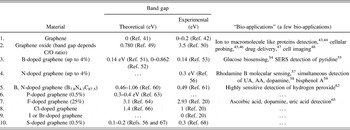
“Heteroatom doping” is another open platform for graphene based sensors, where the functionalities and specificities of the sensors can be tuned by the nature and amount of dopants. Reference Hashim, Narayanan, Romo-Herrera, Cullen, Hahm, Lezzi, R Suttle, Kelkhoff, Munoz-Sandoval, Ganguli, Roy, Smith, Vajtai, Sumpter, Meunier, Terrones, Terrones and Ajayan37 Various heteroatom doped graphenes (a partial list is shown in Table I) were studied for their sensing capabilities toward various bio-analytes. Reference Yang, Zhou, Wu, Cao, Li, Liu and Zhu62,Reference Shao, Zhang, Engelhard, Li, Shao, Wang, Liu, Aksay and Lin69,Reference Guo, Xiao, Liu, Liu, Guo, Gong, Wang and Liu70 Moreover, the presence of defects in graphene will also help for certain graphene based sensors. In all these cases, adsorption of the bio-analytes and the electron transfer kinetics between graphene and biomolecules get modified thereby enabling an augmented sensing capability. Reference Kumar, Min, Bashirzadeh, Barati Farimani, Bae, Estrada, Kim, Yasaei, Park, Pop, Aluru and Salehi-Khojin71,Reference Jeong, Lee, Choi, Lee, Kim, Lee, Lee, Kim and Choi72 The basal plane of the graphene is found to be inert unless it is doped by heteroatoms or defects. On the other hand, the edges are found to be highly reactive. Preferential exposure of the edges by selective vertical growth or preferential arrangement of vertically aligned graphene is also found to be responsible for efficient sensing properties of graphene. Reference Yu, Wang, Lu, Chen, Bo and Chen73,Reference Shang, Papakonstantinou, McMullan, Chu, Stamboulis, Potenza, Dhesi and Marchetto74 Moreover, conjugation of nanoparticles such as gold into graphene also helped the selective and efficient detection of biomolecules. But, detailed studies on the interfaces of graphene and biomolecules is still lacking and this needs to be addressed using various alignments of graphene or by doped graphene, both theoretically and experimentally.
List of a few graphene–bio-interfaces reported.

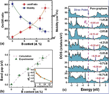
Recently, Terrones et al. reported a density functional theory based study on the effects of external electric field, heteroatoms and defects in graphene in the interaction among dopamine and graphene. Reference Ortiz-Medina, López-Urías, Terrones, Rodríguez-Macías, Endo and Terrones75 This study revealed that the interactions between biomolecules and graphene can be tuned externally, leading to the development of biosensors based on doped graphene. Selective binding of aminoacids to graphene by doping was also theoretically proven via ab initio calculations by Claudio Cazorla. Reference Cazorla76 Hence engineering the graphene by doping opened new avenues in sensors and electronics. Starting from zero band gap pristine graphene (G), one can resort to doping by different atoms to open the band gap of pristine graphene by several eV. Tang et al. have shown the tunable band gaps and transport properties of B-doped graphenes through controllable doping by reaction with the ion atmosphere of trimethylboron decomposed by microwave plasma. Reference Tang, Yin, Yang, Bo, Cao, Wang, Zhang, Bello, Lee, Cheng and Lee77 They argued that the B atoms are substitutionally doped and homogeneously distributed into graphenes without any segregation of B domains. Boron content can be well tuned by adjusting the ion reaction time. The FETs designed using B-doped graphene showed a distinct p-type field-effect behavior with on/off ratios higher with the increase of B content, which augers well for a series of tunable p-type electrical properties. This capability of doping graphenes with predictable transport properties would significantly promote the development of graphene-based FET devices (Fig. 4), and it will benefit the graphene based FET sensors such as bio-analyte sensors.
Tunable electronic properties by of graphene devices by boron doping - (a), (b) tuning the on/off ratio and band gap of graphene, (c) variation in density of states (DOS) upon doping. Reproduced with permission from American Chemical Society. Reference Tang, Yin, Yang, Bo, Cao, Wang, Zhang, Bello, Lee, Cheng and Lee77

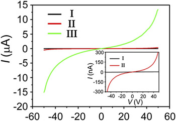
Another highly researched layered material which is analogous to graphene is h-boron nitride (BN), with larger band gap (∼6 eV) and better thermal stability and biocompatibility. Recent work is focused on the band gap variability of BN nanosheets enabling the transition from insulator to metallic material (Fig. 5). Another application was to use BN as an insulating layer from graphene and the copper substrate to facilitate cell growth. Reference Parra, Montero-Silva, Henríquez, Flores, Garín, Ramírez, Moreno, Correa, Seeger and Häberle78 There is an increasing interest in the use of BN-graphene hybrid structures for electronic and optoelectronic applications. Reference Gao, Song, Du, Nie, Chen, Ji, Sun, Yang and Liu79 It was noted that fluorinated BN nanosheets showed current propagation to tens of microamps providing new opportunities in designing and fabricating nanodevices. Reference Xue, Liu, He, Xu, Jiang, Hu and Hu80
Current–voltage (I–V) characteristic curves of bulk BN (I), the exfoliated (II), and fluorinated (III) boron nitride nanosheets (BNNS), respectively; an inset showing the amplified view of the I–V curves (I and II). Reproduced from Springer Publishing Group. Reference Xue, Liu, He, Xu, Jiang, Hu and Hu80

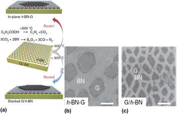
Recent work has focused on the development of both in-plane (h-BN–G) and stacked (G/h-BN) heterostructures containing graphene and h-BN, in the interest of combining their complementary properties for use in a broad range of applications. Varying the concentration of h-BN in h-BN–G is a promising method to tune the graphene band gap. Reference Gao, Song, Du, Nie, Chen, Ji, Sun, Yang and Liu79,Reference Wang, Zhao, Liu and Liu81 It was shown that a novel temperature-triggered reaction route (Fig. 6) in chemical vapor deposition (CVD) process helped to achieve the selective growth of h-BN–G and G/h-BN heterostructures on Cu foils. Reference Gao, Song, Du, Nie, Chen, Ji, Sun, Yang and Liu79
(a) Schematic illustration of the temperature-triggered switching growth between in-plane h-BN–G and stacked G/h-BN heterostructures, defined as Route 1 and Route 2, respectively. (b) SEM image of a sample synthesized by Route 1, showing discrete hexagonal graphene islands embedded in h-BN. (c) Scanning electron microscope (SEM) image of a sample synthesized by Route 2, showing triangular and rhomboidal graphene islands grown on h-BN. The scale bars in b and c are 2 μm. Reproduced with permission from Nature Publishing Group. Reference Gao, Song, Du, Nie, Chen, Ji, Sun, Yang and Liu79

Graphene-based devices on h-BN substrate also exhibit high performance owing to the atomically flat surface of h-BN and its lack of charged impurities. Several computational studies have been reported. A recent paper studied the electric properties, the microscopic dipole polarizabilities and first hyperpolarizabilities of purposely chosen h-BN/graphene nanosized molecular hybrids comprising h-BN segments of increasing size. Reference Karamanis and Pouchan82 The reported quantum chemical computations reveal that size modifications of a h-BN segment confined in a given graphene host may induce dramatic electronic property variations which vary in a rather surprising manner as a function of the graphene host. It was noted that these changes could result in strong nonlinear optical effects that could be used for sensing.
It was shown that computations indicate possible transition from insulating to metallic state of an oxidized BN nanosheet by tuning surface oxygen adsorption by charge injection. Reference Guo and Guo83 Also the insulating nature of BN nanosheets was used to study tunable metal to insulator transitions in double layer graphene heterostructures. Reference Ponomarenko, Geim, Zhukov, Jalil, Morozov, Novoselov, Grigorieva, Hill, Cheianov, Falko, Watanabe, Taniguchi and Gorbachev84
It was noted that in super thin BN cases, the resistivity dramatically drops down to 4.2 × 10² Ω m (compared to 1013 Ω m of commercial pyrolytic BN bulk materials), indicating the electrical properties of super thin BN are dominated by the quantum tunneling effect. Reference Feng, Li, Sajjad, Aldalbahi and Chu85 Also, a recent study showed that atomically thin BN nanosheets can be used as substrates for noble metal particles (Au) for surface enhanced Raman spectroscopy (SERS). Reference Cai, Li, Yu, Liu, Huang, Chen, Watanabe and Taniguchi86 They reported that the Au/BN hybrid enables reusable SERS substrates that can withstand multiple thermal regeneration cycles.
The carrier transport in boron nitride–embedded graphene (BNG) is studied using density functional theory coupled with the Boltzmann transport equation. Reference Wang, Zhao, Liu and Liu81 Under a phonon scattering mechanism, the intrinsic carrier mobility of BNG at room temperature is tunable from 1.7 × 10³ to 1.1 × 105 cm2/(V s) when the band gap is between 0.38 and 1.39 eV. Some specific BNG materials even show ultrahigh mobility up to 6.6 × 106 cm2/(V s), and the transport polarity (whether it is electron or hole transport) can be tailored by the application of a uniaxial strain. The wide mobility variation of BNG is attributed to the dependence of the effective mass and the deformation potential constant on the carbon concentration and width. The results indicate that BNG can have both a large on/off ratio and high carrier mobility and is thus a promising material for electronic devices. Some of these results were confirmed by a recent computational study using a semi classical Monte Carlo method. Reference Hirai, Tsuchiya, Kamakura, Mori and Ogawa87 The electron mobility in graphene is calculated for three different substrates: SiO2, HfO2, and h-BN. They estimated the electron mobility in graphene on the h-BN substrate exhibits a high electron mobility of 170,000 cm2/(V s) for electron densities less than 1012 cm−2. Therefore, the authors state that h-BN should be an appealing substrate for graphene devices, as confirmed experimentally.
An intriguing phenomenon of graphene which enables various applications is amenabilities in controlling its band gap and high carrier mobility. But when the band gap of graphene is opened by doping, its carrier mobility drops dramatically. Opening the band gap slightly, making the on/off ratio non-zero, and still retaining its carrier mobility is a bottleneck. Wang et al. have explored the underlying mechanisms of armchair graphene nanoribbons under phonon scattering by combining first-principles calculations and a tight-binding analysis. Reference Wang, Zhao, Yang, Liu and Liu88 The challenge in making graphene based bio-electronic sensors is with high mobility and large on/off ratio simultaneously limits the development of graphene biosensors. A considerable band gap of up to ∼0.25 eV can be opened up in bilayer graphene by creating a potential difference between the two layers, and thereby breaking the inherent symmetry, if the two layers can be aligned along a certain (Bernal or AB) orientation. Recently, controlled CVD synthesis of wafer-scale AB-stacked bilayer graphene and high-performance transistors have been demonstrated, showing record ON/OFF transistor switching ratio and carrier mobility [as high as 3450 cm2/(V s), which is comparable to that of exfoliated bilayer graphene]. Reference Liu, Krämer, Sarkar, Li, Ajayan and Banerjee89
The understanding and controlling the protein–nanomaterial interfaces will be crucial for designing functional protein–nanomaterial conjugates which will be useful in sensors, fuel, and solar cells. Graphene interacts strongly with proteins and ribonucleic acid (RNA), potentially altering their conformation and disrupting their biological activity. Alva et al. have reported immobilization of Concanavalin A onto a self-assembled monolayer of multivalent tripodal molecules on single-layer graphene Reference Alava, Jason Mann, Théodore, Benitez, William, Parpia and Craighead30 and demonstrated using a quartz crystal microbalance (QCM) to show that tripod-bound Concanavalin A retains its affinity for polysaccharides containing α-d-glucopyrannosyl groups as well as for the α-d-mannopyranosyl groups located on the cell wall of Bacillus subtilis. QCM measurements indicate that adsorption of Concanavalin A onto graphene is accompanied by near-complete loss of these functions which require that interactions with the graphene surface induce deleterious structural changes to the protein. The above studies suggest that other proteins might also be denatured upon adsorption onto graphene which requires that graphene–biomolecules interface must be considered carefully.
Ghoshdastider et al. have reported molecular dynamic (MD) studies of interaction between graphene and glucose oxidase (GOx), Reference Ghoshdastider, Rongliang, Trzaskowskib, Mlynarczykb, Misztab, Gurusaran, Viswanathan, Renugopalakrishn and Filipek90 which has been later used for the design of microfluidic chip for glucose sensing. Reference Viswanathan, Narayanan, Aran, Fink, Paredes, Ajayan, Filipek, Miszta, Tekin, Inci, Demirci, Li, Bolotin, Liepmann and Renugopalakrishanan91 They reported 100 ns all-atom MD simulations of GOx dimer in contact with a single graphene sheet, 7 nm × 7 nm in size, in water environment. The sheet was placed at different sides of the GOx dimer in each simulation. The GOx structure stabilized at about 50 ns, however, the movement of graphene continued until the optimal contact was established around 70 ns. A direct contact of graphene with protein may be potentially hazardous and lead to unfolding of protein. Nevertheless, a close contact between protein and graphene is necessary for obtaining a direct electron transfer from the enzyme active site. Ghoshdastider et al. have examined different shapes of graphene and quantified their ability to wrap the enzyme, GOx dimer. Such an encapsulation leads to the achievement of a high surface contact with graphene, however, the preservation of structure and function of enzyme are challenging and depends on the enzyme shape and location of the substrate binding pocket. The MD simulations revealed that a very tight wrapping of the enzyme is possible but it generates structural changes in the protein, including partial impairment of its catalytic function because of relocation of catalytic residues and cofactor.
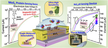
Recently, a novel FET biosensor platform has been demonstrated (Fig. 7) where 2D atomically layered semiconducting membranes made of molybdenum disulphide (MoS2), another extensively researched 2D material, belonging to the class of transition metal dichalcogenides serve as the channel. Reference Sarkar, Liu, Xie, Anselmo, Mitragotri and Banerjee92 Initial investigation has shown that the MoS2-FET biosensors can lead to ultra-high sensitivity, which can surpass that of FET biosensors based on graphene by more than 74-fold. More specifically, a MoS2-based pH sensor achieving sensitivity of 713 for a pH change by 1 unit along with efficient operation over a wide pH range (3–9) was demonstrated. Ultrasensitive and specific protein sensing was also achieved with a sensitivity of 196 even at 100 fM concentration.
Schematic view of an atomically-thin MoS2 based FET biosensor highlighting its ultra-high sensitivity for both protein and pH sensing that beats the sensitivity of graphene based FET biosensors by over 74-fold, its planar platform that promises high-volume/low-cost manufacturability, and its scalability to very small channel lengths that can eventually lead to single molecule detection. Reproduced with permission from American Chemical Society. Reference Sarkar, Liu, Xie, Anselmo, Mitragotri and Banerjee92

The atomically thin nature of MoS2 membranes (mono- or few-layers) with their pristine surfaces lead to excellent electrostatic control and the presence of a finite band gap helps in suppressing the leakage currents, both these factors in combination are instrumental in increasing the sensitivity and reducing the minimum detection limit of the MoS2-FET biosensors. The excellent electrostatics of the MoS2-FETs also allow ultra-low voltage and low off-state-leakage (and hence low power) operation that is desirable for hand-held, battery operated point-of-care biosensors as well as for deployment of such sensor arrays in remote locations. Moreover, similar to graphene, MoS2 offers a planar platform, which can greatly facilitate processing of highly integrated and multiplexed MoS2-FET based sensor architectures. Additionally, it was established through theoretical analysis that MoS2 is greatly advantageous for biosensor device scaling without compromising its sensitivity, which is beneficial for single molecular detection. MoS2 is also highly flexible and transparent and can offer new opportunities in advanced diagnostics and medical prostheses. All these outstanding features make MoS2 a highly promising material for next-generation label-free FET biosensors.
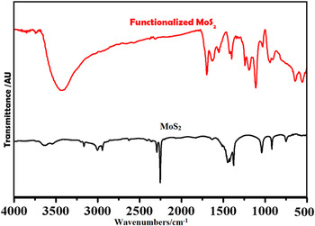
Though MoS2 has been proven as a potential material for various bio-sensing applications, interactions between MoS2 and bio-molecules need to be studied and modified. In one of the theoretical studies, MoS2 is found to be exhibiting van der Waals interactions between a model protein, villin headpiece (HP35)—a commonly used protein for folding studies. Reference Zhou93 The interactions resulted in a robust denaturation of HP35, with protein secondary structure severely destroyed within a few 100 nm simulations. Here also the water molecules play a key role in the adsorption and denaturation process. But these issues can be addressed by suitably modifying the interactions between MoS2 and biomolecules. One such change can be brought by surface modification of MoS2 via oxygen functionalities. Surface functionalized MoS2 resulted from one such functionalization approach Reference Zhou, He, Yang and He94 is shown in Fig. 8. The Fourier transform infrared (FTIR) spectra shown in the Fig. 8 clearly indicate the incorporation of oxygen functionalities [e.g., –OH (∼3400 cm−1) stretching, ester bond (1720 cm−1) etc.] in MoS2. But a detailed study on the interaction between biomolecules and functionalized MoS2 needs to be conducted to unravel these effects.
FTIR spectra of MoS2 and functionalized MoS2.

I. CONCLUSION
New chemical sensor systems are being developed at an incredible fast pace due to the emergence of new smart materials including carbon-based platforms, capable of amplifying electrical signals from charge transfer probe molecules, engineered for specific applications. The emerging 2D nanomaterials have been proposed as key components in sensing since they confer distinctive advantages over conventional transducers. In particular, the characteristic electronic and optical properties of carbon and noncarbon 2D materials are potentially significant in sensing. The unique chemical and physical properties of graphene, its functional derivatives and other 2D materials offer opportunities to functionalize and append probe proteins, micro RNA, viruses, antibodies for use in sensing. These materials have unique properties, including the potential for transduction mechanisms that make them attractive for in vitro and in vivo sensors that can be used for health monitoring and disease therapy outcomes. Clinical applications include continuous glucose monitors, bacteria, virus detection, to name a few. Biosensing is of paramount importance in improving the quality of human life. Biosensors are able to detect a wide range of molecular species with enhanced sensitivity and selectivity, typically in pico molar range with applications in security, point-of-care analyses of diseases, and environmental safety. Here a brief account on the importance of various 2D materials–biomolecule interfaces is provided. In addition, recent demonstration of MoS2 FET as an attractive platform for next-generation label-free biosensors is highlighted. An understanding of bionano materials interface is important for the development of these 2D nanomaterials based new generation biosensors.
ACKNOWLEDGMENTS
K.K.T. and T.N.N. acknowledge TIFR-Centre for Interdisciplinary Sciences (TCIS), Hyderabad, India for the financial support. V.R. and S.V. acknowledge Rothschild Foundation for support of our research.