I. INTRODUCTION
Molecular self-assembly represents an efficient bottom-up strategy to generate stable and structurally well-defined aggregates in which the molecular building blocks are held by noncovalent interactions under thermodynamic control and supramolecular design rules.Reference Whitesides, Mathias and Seto1, Reference Lehn2 This approach has been used to fabricate desired nanostructures of semiconducting π-conjugated materialsReference Meijer and Schenning3–Reference van Hameren, Schon, van Buul, Hoogboom, Lazarenko, Gerritsen, Engelkamp, Christianen, Heus, Maan, Rasing, Speller, Rowan, Elemans and Nolte8 on surfaces that are tailored for different types of organic electronic devices such as photovoltaicsReference Schmidt-Mende, Fechtenkotter, Mullen, Moons, Friend and MacKenzie9–Reference Neuteboom, Meskers, van Hal, van Duren, Meijer, Janssen, Dupin, Pourtois, Cornil, Lazzaroni, Bredas and Beljonne11 and field-effect transistors.Reference Pisula, Menon, Stepputat, Lieberwirth, Kolb, Tracz, Sirringhaus, Pakula and Mullen12–Reference Jonkheijm, Stutzmann, Chen, de Leeuw, Meijer, Schenning and Wurthner18 For efficient charge transport, the one-dimensional (1D) organization of π-conjugated molecules with long-range ordering is desired. Several strategies have been adapted to produce such organization on surfaces. The most commonly used approach is to transfer the preorganized stacks of π-conjugated materials, formed under equilibrium conditions in solution, to surfaces by solution casting. Such a method usually results in randomly aligned nanowires and all the interactions between the stacks and specific surfaces needed to be considered.Reference Wurthner, Thalacker and Sautter19–Reference Jonkheijm, van der Schoot, Schenning and Meijer26 To achieve surface structure with a high degree of alignment of the 1D stacks, several advanced material processing techniques including surface dewetting,Reference Meijer and Schenning3 zone-casting,Reference Pisula, Menon, Stepputat, Lieberwirth, Kolb, Tracz, Sirringhaus, Pakula and Mullen12 stamp-assisted deposition,Reference Cavallini, Stoliar, Moulin, Surin, Leclere, Lazzaroni, Breiby, Andreasen, Nielsen, Sonar, Grimsdale, Mullen and Biscarini14 thermal treatment,Reference Xiao, Myers, Miao, Sanaur, Pang, Steigerwald and Nuckolls15 flow-induced alignment,Reference Raez, Moralez and Fenniri27 magneticReference Shklyarevskiy, Jonkheijm, Stutzmann, Wasserberg, Wondergem, Christianen, Schenning, de Leeuw, Tomovic, Wu, Mullen and Maan13, Reference Shklyarevskiy, Jonkheijm, Christianen, Schenning, Guerzo, Desvergne, Meijer and Maan28, Reference Lee, Choi, Pate, Chisholm and Han29 and electric field-assisted alignmentReference Messmore, Hulvat, Sone and Stupp30, Reference Sardone, Palermo, Devaux, Credgington, de Loos, Marletta, Cacialli, van Esch and Samori31 have been demonstrated. These approaches involve both kinetic control, such as solvent drying rate and surface diffusivity, during the material deposition and thermodynamic control through supramolecular design rules, which dictate the final supramolecular structure with the lowest free energy.
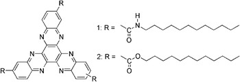
Driven by the need to develop n-type supramolecular nanowires,Reference Schenning and Meijer5, Reference Yip, Zou, Ma, Tian, Tucker and Jen32 our work here has been focused on two rationally designed derivatives of an n-type π-conjugated hexaazatrinaphthylene (HATNA) molecule. HATNA is an electron-deficient discotic molecule with C 3h symmetry and well-defined face-to-face columnar packing in its crystal structure.Reference Du, Bu and Biradha33 HATNA-based materials have been theoreticallyReference Lemaur, da Silva Filho, Coropceanu, Lehmann, Geerts, Piris, Debije, van de Craats, Senthikumar, Siebbeles, Warman, Bredas and Cornil34 and experimentallyReference Lehmann, Kestemont, Aspe, Buess-Herman, Koch, Debije, Piris, de Hass, Warman, Watson, Lemaur, Cornil, Geerts, Gearba and Ivanov35, Reference Kaafarani, Kondo, Yu, Zhang, Dattilo, Risko, Jones, Barlow, Domercq, Amy, Kahn, Bredas, Kippelen and Marder36 shown to have high charge-carrier mobility, making them potential candidates for organic electronic devices. Herein, we report the self-assembling properties of HATNA-1 and HATNA-2 (Fig. 1) in different solutions and their corresponding organization on surfaces. In addition, we exploit the versatility of solvent-vapor annealing (SVA) as a post-treatment method to control the surface organizations of the supramolecular nanowires. SVA is a physical process that facilitates the transformation of organic materials from kinetically trapped states into thermodynamically stable states. This method had been used to control the growth of organic semiconductor crystals,Reference Conboy, Olson, Adams, Kerimo, Zaban, Gregg and Barbara37, Reference Mascaro, Thompson, Smith and Bulovic38, Reference Dickey, Anthony and Loo39 to generate nanowires from π-conjugated molecules and polymers,Reference Datar, Oitker and Zang40–Reference Kim, Jang, Park and Cho43 and to perfect the ordering in block-copolymer thin films.Reference Kim, Misner and Russell44, Reference Xuan, Peng, Cui, Wang, Li and Han45
Molecular structure of HATNAs. HATNA-1 and HATNA-2 are tethered with ester-dodecyl groups and amide-dodecyl groups, respectively.

II. EXPERIMENTAL SECTION
A. Materials
All solvents [high-performance liquid chromatography (HPLC) grade] used in this study except ethanol were purchased from EMC Corp., Camp Hill, PA. The 1-octadecanethiol (ODT) was purchased from Aldrich, St. Louis, MO, and used as received. Absolute (200 proof) ethanol (Aaper Alcohol and Chemical Company, Shelbyville, KY) was used for making thiol solutions for μCP.
B. Substrates
SiO2 (300-nm thermal oxide)/antimony-doped Si substrate was purchased from Montco Silicon (Spring City, PA) and cleaned with acetone and isopropanol before use. Polycrystalline gold substrates were prepared by electron beam evaporation of gold (25 nm thick, 99.999%; Kurt J. Lesker Company, Pittsburgh, PA.) onto Si(100) wafers that had been primed with a layer of titanium (1 nm thick, 99.995%; Kurt J. Lesker Company) to promote adhesion between silicon and gold. Electron beam evaporation (SEC 6000, CHA Industries, Fremont, CA) of gold was performed under high vacuum with pressure of 1 × 10⁻⁶ Torr at a rate of 0.1 nm/s. The root mean square roughness of Au structure is equal to 0.6 ± 0.2 nm and an average grain diameter of 20–40 nm. A typical photolithography procedure was used to prepare the substrate for a bottom contact field-effect transistor. The drain and source electrodes were formed by thermal evaporation of 5 nm of chromium and 40 nm of gold.
C. Instrumentation
Ultraviolet-visible (UV-vis) absorption spectra were recorded using a Perkin-Elmer (Waltham, MA) Lambda 9 spectrophotometer. Digital Instruments Multimode Nanoscope III scanning probe microscope (Veeco, Santa Barbara, CA) installed with etched silicon tips and a typical resonant frequency of 300–350 kHz was used to perform the atomic force microscopy (AFM) studies. Scanning electron microscopy (SEM) images were taken using a JEOL (Tokyo, Japan) field-emission scanning microscope (JSM-7000F) at operating voltage of 10 kV.
D. Microcontact printing
A micropatterned photoresist film, fabricated by photolithography, was used as a master to replicate stamps for microcontact printing. Masters were coated with a self-assembled monolayer (SAM) of (1, 1, 2, 2-tetrahydroperfluorodecyl)trichlorosilane (Sigma-Aldrich, St. Louis, MO) to ensure a clean release of the cured stamp. A typical stamp was made by casting a 10:1 (v/v) mixture of polydimethyl siloxane (PDMS) and curing agent (Sylgard 184, Dow Corning, Midland, MI) against a silanized master in an oven at 60 °C for 20 h. For μCP of ODT on Au substrate, 2 mM of ODT in ethanol was dispersed on the patterned PDMS stamp for 60 s and then dried under a nitrogen stream. The stamp was then allowed to form conformal contact with the Au substrate for 5 s.
E. SVA
The target samples and a glass vial containing 20 mL of solvent were stored together in a sealed glass container (300 cc) for different periods of time. All the samples were allowed to dry in air for at least 2 h before AFM study.
III. RESULTS AND DISCUSSION
A. Self-assembly in solutions
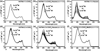
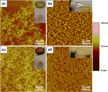
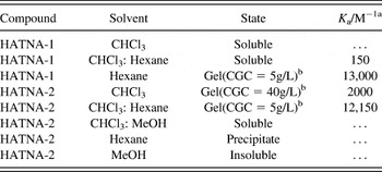
The self-assembling properties of HATNA-1 and HATNA-2 in solutions were studied by concentration-dependent UV-vis absorption experiments. The corresponding average association constant K a at different solvent systems calculated from the concentration-dependent spectral changes using the isodesmic model is summarized in Table I. This method is commonly used to study the self-assembling property of the supramolecular system with linear sequence.Reference Martin46, Reference Wurthner, Thalacker and Sautter47 Chloroform is a good solvent for both the HATNA moiety and its aliphatic substituted derivatives. As a result, HATNA-1 was completely dissolved in CHCl3 [Fig. 2(a)]. When hexane was used as solvent, concentration-dependent spectral changes that derived from the dynamic exchange between monomer and aggregate species were observed. Upon increasing concentrations, all the characteristic peaks decreased in absorbance [Fig. 2(c)]. The decrease of the ratio of peak intensity between the 0–0 (392 nm) and 0–1 (374 nm) transitions and a hypsochromic shift of the main peak from 296 to 292 nm upon concentration increase indicates the formation of H-aggregates.Reference Yip, Zou, Ma, Tian, Tucker and Jen32, Reference Ishi-i, Yaguma, Kuwahara, Taguri and Mataka48 The calculated association constant K a for HATNA-1 in hexane at room temperature is 13,000 M−1. A further increase of the concentration of HATNA-1 in hexane resulted in the formation of a gel. An AFM morphology study of the gel deposited on SiO2/Si substrate revealed that HATNA-1 aggregated into a nanowire network [Fig. 3(a)]. When HATNA-1 was deposited from its dissolved state from CHCl3, an amorphous thin film was formed [Fig. 3(b)].
Concentration-dependent UV-vis measurements of HATNA-1 in (a) CHCl3, (b) CHCl3/hexane(v/v = 1:1), (c) hexane, and HATNA-2 in (d) CHCl3, (e) CHCl3/hexane(v/v = 1:1), (f) CHCl3/MeOH (v/v = 1:1). The concentration varied from 1 × 10⁻⁴ M to 3 × 10⁻⁶ M in all cases.

Tapping-mode AFM images of HATNA-1 spin-coated from (a) hexane, (b) CHCl3, and HATNA-2 spin-coated from (c) CHCl3/hexane (v/v = 1:1), (d) CHCl3 on SiO2/Si. The spin speed and concentration in all the cases were 3000 rpm and 5 g/L, respectively. The thickness of the thin films in (b) and (d) is between 20 and 30 nm.

Solvation states and association constants (K a) of HATNA-1 and HATNA-2 in different solvents.

a K a is calculated using the isodesmic (or equal K) model based on the concentration-dependent UV-vis absorption spectrum.
b Critical gelation concentration (CGC) is the lowest gelator concentration at which gelation is still observed.
With the introduction of amide groups, the 1D self-assembly of HATNA-2 is reinforced because both the coplanar π–π stacking between the disoctic cores and the directional hydrogen bonds between the amide groups of adjacent molecules are favorable for the formation of nanowires. The interactions between the aliphatic side chains play a relatively minor role in the self-assembly of HATNA-2 because the strength of van der Waals force is much weaker than those of π–π stacking and hydrogen bonds.Reference Hoeben, Jonkheijm, Meijer and Schenning6 HATNA-2 could be dissolved in CHCl3 at high concentrations (>50 g/L), however the solution slowly gelled over a few days. The UV-vis absorption study showed that HATNA-2 formed aggregates in CHCl3 with a K a of 2000 M−1 [Fig. 2(d)]. By adding a more polar solvent such as methanol into this CHCl3 solution, it resulted in the breakdown of the aggregations through the weakening of interactions between H-bonding of amides [Fig. 2(f)]. HATNA-2 could be dissolved in hexane when the solution was slightly heated; however, it precipitated out instead of gelling when the solution was cooled to room temperature. A cosolvent of CHCl3/hexane (v/v = 1:1) provided a suitable environment for HATNA-2 to self-assemble, a visually clear gel was formed within an hour when HATNA-2 was cooled from the warmed solution. The concentration-dependent absorption spectral changes of HATNA-2 in CHCl3/hexane were similar to that of HATNA-1 with the main peak blue-shifted by 8 nm from 304 to 296 nm when the concentration was increased from 3 × 10⁻⁶ M to 1 × 10⁻⁴ M, which indicated that HATNA-2 also self-assembled in the form of H-aggregates [Fig. 2(e)]. The AFM studies of HATNA-2 prepared from the gel revealed the formation of a nanowire network. However, the nanowires of HATNA-2 were much less entangled when compared to that of HATNA-1 [Fig. 3(c)]. This difference in morphology was due to the enhancement of the molecular interactions between the directional H-bonding, which increased the stiffness of the nanowires of HATNA-2 and reduced the chance of coiling. Spin casting of the freshly prepared CHCl3 solution of HATNA-2 on SiO2/Si substrate resulted in thin film composed of small grains in which HATNA-2 were self-organized with short-range ordering. Both surface organization of HATNA-1 and HATNA-2 prepared from their good solvents can be considered as kinetically trapped structures that are far from equilibrated.
B. SVA-induced self-assembly on surfaces
Although the self-assembling mechanisms and properties of the supramolecular structures in solution have been extensively studied, the capability of using post-treatment to control the self-organization at their solid phase is comparatively unexplored.Reference Datar, Oitker and Zang40, Reference De Luca, Liscio, Maccagnani, Nolde, Palermo, Mullen and Samori41 Herein, we also studied the effect of SVA on the reorganization of the self-assembled molecules on surfaces. In previous reports,Reference Datar, Oitker and Zang40, Reference De Luca, Liscio, Maccagnani, Nolde, Palermo, Mullen and Samori41 SVA had been used to transform small aggregates of perylene diimide derivatives into millimeter-long fibers with submicron-width through a nucleation and growth process. During the SVA process, the solvent molecules are absorbed by the deposited layer and the substrate, leading to self-healing of imperfect organization in the deposited layer and eventually formed thermodynamically stable crystalline morphologies.Reference De Luca, Liscio, Maccagnani, Nolde, Palermo, Mullen and Samori41 In our study, several parameters were used to manipulate the annealing process in these experiments, including the initial organization of the molecules, the type of solvent vapor used for annealing, and the annealing time to provide a systematic study of the SVA effect on the resulting morphology of HATNA-2. AFM was used to monitor the change of surface organization at different annealing stages to reveal the self-assembling mechanism.
1. Formation of randomly aligned nanowires
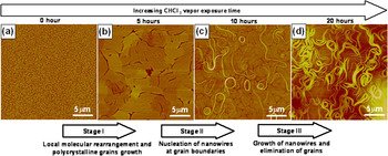
A thin film of HATNA-2 was first prepared by spin coating from its CHCl3 solution on SiO2/Si or Au substrates. As mentioned previously, a poorly organized morphology was formed under this preparation condition. When the thin film was exposed to a saturated vapor of CHCl3 at room temperature, changes of surface morphology were observed. A series of AFM images in Figs. 4(a)–4(d) show the transformation of the surface structures at different stages of SVA. The absorption of CHCl3 vapor by the thin film and substrate imparted physical mobility to the molecules, which led to the slow rearrangement of the kinetically trapped amorphous structure into a more thermodynamically favorable ordered structure. This is presumably the 1D arrangement originating from the directional H-bonding and π–π stacking.
(a–d) Tapping-mode AFM images of HATNA-2 at different CHCl3 vapor annealing stages. The starting thin film was prepared from spin coating a solution of HATNA-2 (10 g/L) in CHCl3 on SiO2/Si at 3000 rpm. The sample was exposed to saturated CHCl3 vapor for a different period of time and then dried in air before imaging.

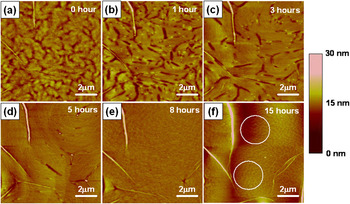
The growth dynamic of the nanowires was investigated by monitoring the morphological changes of HATNA-2 under the same area at different SVA times using AFM [Figs. 5(a)–5(f)]. During stage I of SVA, the film started to absorb the solvent vapor and the original poorly arranged molecules underwent local rearrangement and started to interact with adjacent molecules to form crystalline domains. Within the first hour of SVA, the size of the domains was smaller than 2 μm [Figs. 5(a) and 5(b)]. These domains continued to grow into polycrystalline grains, which were composed of oriented molecules with stacking axis parallel to the surface after a longer annealing time. The typical driving force for grain growth was the reduction of the total area of the energetic grain boundaries.Reference Liu49 This process was evident by the observation of typical grain growing phenomena, including grain-boundary diffusion, elimination, and grain coarsening [Figs. 5(b)–5(d)]. Between 5 and 10 h of annealing, the grains reached a maximum size of several micrometers at which point stage II begins.
(a–f) Tapping-mode AFM images of HATNA-2 at different CHCl3 vapor annealing stages. The starting thin film was prepared from spin coating a solution of HATNA-2 (10 g/L) in CHCl3 on SiO2/Si at 3000 rpm. The AFM images were obtained by scanning the same area of the thin film using a few of the preorganized nanowires as mapping sites. Circles highlight the surface dewetting region of HATNA-2.

During stage II of SVA, the polycrystalline thin film continued to absorb the solvent vapor and the morphology showed a smoothening of grain surfaces and boundaries after ~8 h of annealing [Fig. 5(e)]. The thin film appeared to reach a metastable supersaturation state, which was the precondition for the nucleation and growth of a crystalline phase. After a longer annealing time, the nucleation of the crystalline nanowires of HATNA-2 was observed at the grain boundaries, which were the preferable sites for solid phase nucleation due to their high local energetic nature.Reference Liu49 Two types of nuclei were observed including closed-loop type nanowires formed at the peripheral of single grains and open-end nanowires formed along the boundaries over several grains [Fig. 4(c)].
During stage III of SVA, the nanowire nuclei started to grow by a continuous collection of molecules from the mother phase (the polycrystalline grains) to the surface of the crystalline nanowires. Consequently, some molecules started to dewet from the surface [Fig. 5(f)] and eventually resulted in a surface devoid of grains with only a network of nanowires remaining. The widths of the nanowires were in range of 20–100 nm and the length could be >100 μm based on the AFM [Fig. 4(d)] and SEM studies [Fig. S1 in Supporting Information]. In addition, the nanowires did not readily crossover each other because it was an unfavorable state that creates high-energy interface between two misoriented crystalline phases. This type of morphology was very different from the nanowire networks obtained by the direct transfer of preorganized nanowire stacks from solution to the surface of substrates [Fig. 3(c)]. The similar nucleation and growth of nanowires was also observed when Au substrates were used.
The annealing effect of different solvent-vapor systems on the reorganization of HATNA-2 was also studied and is summarized in Fig. S2 in Supporting Information. Both MeOH and hexane were poor solvents for HATNA-2 in solution-based self-assembly and their corresponding vapors also did not significantly affect the self-assembly of HATNA-2 on the surface. However, the MeOH vapor competed with the amide H-bonding in HATNA-2, which resulted in an even more disorganized morphology while the hexane vapor showed no observable effect on the reorganization of HATNA-2. When the thin film was exposed to the vapor mixtures of CHCl3:MeOH and CHCl3:hexane, only short range reorganization of HATNA-2 were observed. These results suggested that only thermodynamically compatible solvent vapor provides synergic interactions with the self-assembling molecules and transforms the kinetically trapped organization into supramolecular assemblies.
2. Formation of preferentially aligned nanowires
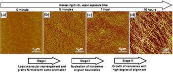
Thin films composed of different preorganizations of HATNA-2 were also used to study the SVA effect. The nanowire network deposited from the gel of HATNA-2 is a stable structure. By exposing this robust structure to CHCl3 vapor, we did not observe an obvious destructive change of the network organization [Fig. S3 in Supporting Information]. However, when the initial thin film was prepared from spin coating of a warm solution of HATNA-2 in CHCl3/hexane (v/v = 1:1) at 60 °C, a smooth surface with a small amount of aggregation was observed [Fig. 6(a)]. This partial aggregation phenomenon in solution was also evident in the temperature-dependent UV-vis study [Fig. S4 in Supporting Information]. When SVA was applied to this thin film, a characteristic morphological change was observed [Figs. 6(a)–6(d)].
(a–d) Tapping-mode AFM images of HATNA-2 at different CHCl3 vapor annealing stages. The starting thin film was prepared from spin coating a solution of HATNA-2 (10 g/L) in CHCl3:hexane (v:v = 1:1) at 60 °C on SiO2/Si at 3000 rpm.

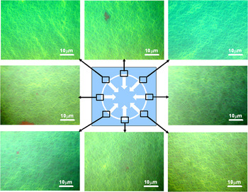
After 5 min of vapor annealing, small grains with preferential grain direction started to develop and the nucleation of nanowires at the grain boundaries also occurred [Fig. 6(b)]. These nanowires continued to grow along the same direction of the grains for longer annealing time and eventually all the grains disappeared leaving well-aligned nanowires on the surface [Figs. 6(c) and 6(d)]. More interestingly, the morphological study of different areas on the substrate revealed that the alignment direction of the nanowires were parallel to the radial direction of the substrate (Fig. 7), which was also the drying direction of the solvent meniscus that moved from the edge toward the center of the substrate during the drying stage of spin coating. We propose that the driving force for the formation of aligned nanowires is originated from the drying-induced prealignment of small aggregates on the substrate during the spin-coating process. A similar spin coating induced arrangement of aggregates has also been reported in another supramolecular system.Reference Yamaguchi, Kimura, Matsuda and Aida50 Because the thin film prepared from a warm CHCl3/hexane (v/v = 1:1) solution contained some partially aggregated HATNA-2, the SVA time required for the nucleation and growth of nanowires was reduced compared to the amorphous one prepared from CHCl3 solution.
Optical images of the aligned nanowires captured from different positions of the substrate. The sample was prepared from spin coating a solution of HATNA-2 (10 g/L) in CHCl3:hexane (v:v = 1:1) at 60 °C on SiO2/Si at 3000 rpm followed by 10 h of CHCl3 vapor annealing. The white arrows in the middle figure show the drying path of the solution during the spin coating. We observed that the nanowires aligned with the same direction as the solvent drying path.

To take this one step further, we prepared the nanowires on SiO2/Si substrate prepatterned with Au electrodes in a bottom contact field-effect transistor configuration, we were able to grow and align the nanowires across the electrodes using the SVA method (Fig. S5 in Supporting Information). However, there was no measurable electrical property obtained from those devices. This may be due to the poor contact or large injection barrier between the Au electrodes (work function = 5.1 eV) and HATNA-2 nanowires [lowest unoccupied molecular orbital (LUMO) = 3.4 eV]. Further improvement between the contact as well as the charge injection properties between the electrodes and the nanowires are needed to fully explore the potential of using these aligned nanowires for supramolecular electronics.
C. Patterning of nanowires
Patterning of organic semiconductor is very important for fabricating high-performance electronic devices. A soft lithographic techniqueReference Xia and Whitesides51 such as microcontact printing has been demonstrated as a simple and effective way to pattern organic semiconductors.Reference Park, Shim and Lee52–Reference Briseno, Mannsfeld, Ling, Liu, Tseng, Reese, Roberts, Yang, Wudl and Bao57 To pattern the nanowires on SiO2/Si and Au substrates, we have used the combined SVA and microcontact printing approaches.
1. Nanowire patterns generated from microcontact printed thin film
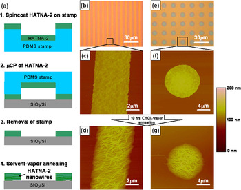
A thin film of molecule HATNA-2 was first spin-coated from its warm CHCl3/hexane (v/v = 1:1) solution onto a patterned PDMS stamp. The stamp was then allowed to form conformal contact with an oxygen plasma-treated SiO2/Si substrate for 30 s to transfer the thin film onto the surface [Fig. 8(a)]. Figures 8(b) and 8(e) are the optical images and Figs. 8(c) and 8(f) are the corresponding AFM morphologies of the thin films printed from the PDMS stamps with 5 μm × 5 μm line features and 10 μm circle feature, respectively. The as-prepared thin film showed a smooth and amorphous surface structure, which was very similar to that obtained from direct spin coating of HATNA-2 on SiO2/Si substrate. A patterned array of nanowires was formed subsequently when the micropatterned thin film was exposed to CHCl3 vapor [Figs. 8(d) and 8(g)]. This technique is also generally applicable to other substrates including Au and glass.
(a) Schematic drawing of the mechanism for patterning nanowires on SiO2/Si substrate. (b, e) Optical images of the patterned thin film of HATNA-2 with 5-μm line feature and 10-μm circle feature, respectively. AFM images of HATNA-2 in line pattern (c) before and (d) after CHCl3 vapor annealing for 10 h and HATNA-2 in circle pattern (f) before and (g) after CHCl3 vapor annealing for 10 h.

2. Nanowire patterns generated from selective surface dewetting
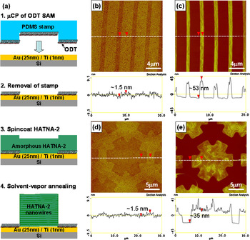
Microcontact printing of a molecular monolayer on a substrate can generate patterned regions with different surface wettability. This patterned substrate has been used to fabricate arrays of π-conjugated polymer thin films through selective surface wetting or dewetting of the polymer during the inkjet printingReference Wang, Zheng, Li, Huck and Sirringhaus58 and dip-coating process.Reference Briseno, Roberts, Ling, Moon, Nemanick and Bao53, Reference Chabinyc, Wong, Salleo, Paul and Street59 When this technique was combined with SVA, an originally amorphous thin film of HATNA-2 could be transformed into a patterned array of supramolecular nanowires [Fig. 9(a)]. This experiment started with the patterning of a monolayer of ODT on an Au surface through microcontact printing to create a patterned surface with different wettability. An amorphous thin film of HATNA-2 with thickness of ~20 nm was then spin-coated from its CHCl3 solution on the substrate, which has different ODT patterns. The morphology of these films almost totally replicates those of the underneath SAM patterns [Figs. 9(b) and 9(d)]. When the samples were further exposed to a saturated CHCl3 vapor, the molecules started to self-organize. Meanwhile, the absorbed CHCl3 started to dewet the low surface energy ODT regions and carried the HATNA-2 onto the Au region, which resulted in a patterned array of nanowires [Figs. 9(c) and 9(e)].
(a) Schematic drawing of the patterning mechanism of nanowires on Au substrate printed with a molecular monolayer template. (b, d) AFM images of the amorphous thin film of HATNA-2 spin-coated from (10 g/L) CHCl3 at 3000 rpm on 1 μm (Au region) × 3 μm (ODT region) line pattern and ODT star pattern, respectively. (c, e) Corresponding AFM images of (b) and (d) after 10 h of CHCl3 vapor annealing.

IV. CONCLUSIONS
In summary, our study shows that in addition to the widely used solution-based self-assembling methods, SVA offers an alternative way to control the organization of supramolecular nanowires on surfaces. The kinetically trapped structures can be transformed into self-assembled nanowire structures through a nucleation and growth mechanism when they are exposed to a compatible solvent vapor. Several parameters including the preordering in the starting materials, choice of solvent vapor, and the annealing time can be tuned to create different supramolecular organizations on surfaces. When combining the SVA and microcontact printing methods, patterned arrays of nanowires can be achieved on different substrates. We believe that this simple material processing approach should be generally applicable to other self-assembled 1D organic semiconducting system to generate desired organization for organic electronic devices.
ACKNOWLEDGMENTS
This work is supported by the National Science Foundation (the NSF-STC Program under Agreement No. DMR-0120967), Air Force Office of Scientific Research (AFOSR) under the Bio-inspired Concept Program. A.K.Y. Jen thanks the Boeing-Johnson Foundation for financial support. H.L. Yip acknowledges the Intel Foundation Fellowship and the Nanotechnology Fellowship sponsored by the University Initiative Fund (UIF) from the Center for Nanotechnology at the University of Washington, a member of the National Nanotechnology Infrastructure Network (NNIN) supported by NSF.