
I. INTRODUCTION
Organic semiconductors have played an integral role in the development of cheap, reliable, and efficient electronic devices. The organic light emitting diodes, organic photovoltaics, and organic field effect transistors (OFETs) have already found their way into the consumer mass market. Reference Brown, Jarrett, de Leeuw and Matters1–Reference Sirringhaus4 Due to their mechanical flexibility, room temperature processing, large area depositions, biodegradability, and low processing costs, organic semiconductors have proven useful in developing novel applications over the past few decades.
This has resulted in various innovations such as flexible displays, Reference Yagi, Hirai, Miyamoto, Noda, Imaoka, Yoneya, Nomoto, Kashara, Yumoto and Urabe5 electronic skin and fabric, Reference Schwartz, Tee, Mei, Appleton, Kim, Wang and Bao6 cheap and disposable RFID tags, Reference Tinivella, Camarchia, Pirola, Shen and Ghione7 anti-counterfeiting banknotes, Reference Zschieschang, Yamamoto, Takimiya, Kuwabara, Ikeda, Sekitani, Someya and Klauk8 as well as biosensors. Reference Liao and Yan9
The trend of miniaturization of complementary metal-oxide-semiconductor (CMOS) electronics has brought about a quasi-ubiquitous electronics revolution. However, a truly-ubiquitous electronic world is yet to be achieved, where electronics are no longer confined to planar surfaces but are allowed to be placed onto any arbitrarily shaped and dynamic surface. Continuing research on improving mechanical reliability in an extreme and repeated flexure, on optimizing the organic fabrication procedures, as well as on reducing processing costs is needed for the widespread adoption of organic electronics. Reference Yang, Yoon, Kim, Hong, Chung, Heo, Park and Ree10 A further trend for truly ubiquitous electronics is also required, in which the organic electronic devices are designed to be highly versatile in their performance. In terms of transistor behavior, OFETs have already consistently achieved a mobility between 0.01 and 10 cm2/(V s), with single crystal 5,6,11,12-tetraphenyltetracene (rubrene) OFETS pushing 40 cm2/(V s). Reference Jurchescu, Popinciuc, van Wees and Palstra11 This performance is comparable or even surpasses that of typical hydrogenated amorphous Si (a-Si:H) thin film transistors (TFTs) used in liquid-crystal displays. Reference Karim, Servati and Nathan12 Here, we have focused our attention on designing an organic thin film transistor (OTFT) for a wide range of operating conditions to allow for high-voltage (HV) applications.
High voltage (>100 V) is not well explored in the area of organic semiconductors and could help enable applications that would not exist otherwise. A high-voltage transistor is one that drives voltages above 100 V across its source and drain while being controlled by a relatively smaller gate to source voltage V GS. The idea behind a high-voltage organic thin film transistor (HVOTFT) is to integrate it with flexible capacitive MEMS actuators, all fabricated on shapeshifting plastic shells or fabrics. With large voltages being driven to a MEMS actuator, microscale and macroscale capacitive actuation can be achieved on surfaces that would normally otherwise be static. Transportation vehicle bodies, high-tech body armor, and consumer goods could all potentially be shapeshifted, under a large electromagnetic force, for cosmetic or practical applications. High-voltage drivers can also be utilized in novel display systems such as ferroelectric liquid crystals, electrophoretic or electro-optic displays, or even tactile MEMS-based braille sheets. Reference Unagami and Kogure13–Reference Kato, Sekitani, Takamiya, Doi, Asaka, Sakurai and Someya16 Digital X-ray imaging is yet another application in which a high-voltage OTFT can be of use. The flat panel detector would be replaced with a flexible “bed sheet” detector with incorporated high-voltage organic thin film transistors (HVOTFTs), which would allow for high-voltage fault detection as well as doubling up as an actual blanket for the patient. Reference Karim, Servati and Nathan12,Reference Zhao, Law, Waechter, Huang and Rowlands17
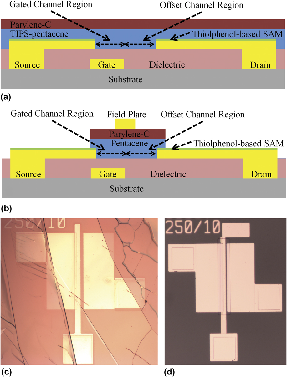
In this work, we have demonstrated high-voltage organic TFTs with gated channel lengths between 5 and 30 μm. HVOTFTs were fabricated with both nonvacuum solution-processed and vacuum-deposited organic semiconductors, with either a high-k or an organic dielectric layer. The high-voltage operation is enabled by designing an offset semiconductor channel region between 5 and 30 μm long that is in series with the gated channel region. The offset channel region accommodates the large potential drop between the source and drain, while the gated channel region accumulates the charge and enables the transistor behavior. HVOTFTs have been made with both 6,13-bis(triisopropylsilylethynyl)pentacene (TIPS-pentacene) and pentacene organic semiconductors, capable of driving voltages up to −150 V and −550 V, respectively. For TIPS-pentacene, mobilities of 0.018 cm2/(V s) have been achieved; however, relatively low I on/I off current ratios were measured. Pentacene HVOTFTs had a lower mobility of 0.00025 cm2/(V s) but with significantly higher I on/I off current ratios on the order of 1 × 10⁶. The reliability of the dielectric layers and the performance of the HVOTFT fabricated on polyimide substrates were analyzed under the flexure. Various fluorinated and nonfluorinated thiolphenol-based surface-assembled monolayers were also used to coat the metal source and drain contacts to improve charge injection into the semiconductor. Finally, a top field plate design was added to help control the hole charge accumulation within the organic semiconductor channel.
II. DEVICE FABRICATION AND EXPERIMENT
A. Device fabrication
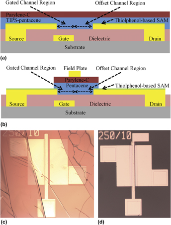
The cross-sectional diagram and the top-down views of the HVOTFTs are shown in Fig. 1. HVOTFTs were fabricated on 100 mm borosilicate glass (Valley Design Corporation, Shirley, Massachusetts) and flexible Kapton PV9101 (Dupont, Circleville, Ohio) polyimide substrates. The patterned wafers were eventually diced into 1 inch squares, allowing for multiple samples to be fabricated with different self-assembled monolayer (SAM), dielectrics, and organic semiconductors. The samples are summarized in Table I, with each having 400 individual devices. The glass substrates were precleaned by a piranha solution for 30 min, while the Kapton substrates were submerged sequentially in acetone and isopropyl alcohol in an ultrasonic bath for 30 min, both followed by a DI water rinse. The glass and Kapton substrates were then heat treated at 100 °C in a convection oven for 1 h for surface dehydration and thermal stability, respectively.
Cross-sectional diagrams of the HVOTFT with the gated and offset channel regions for (a) TIPS-pentacene and (b) pentacene devices. TIPS-pentacene was deposited via a drop-casting method while pentacene was vacuum deposited. Additionally, a field plate was added on top of the parylene-C encapsulation layer for the pentacene devices. (c) Optical micrograph of TIPS-pentacene crystals covering patterned metal contacts. (d) Optical micrograph of a pentacene HVOTFT with a top field-plate.

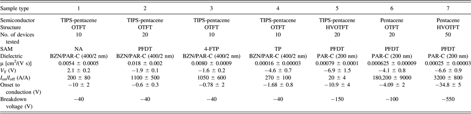
Comparison of the electrical properties of the OTFTs and HVOTFTs.

A bottom gate and bottom contact architecture was adopted to avoid thermal evaporating metal contacts on top of the sensitive organic semiconductor. This would prevent unnecessary damage to the sensitive organic semiconductor. This also allowed for a final drop-cast solution-processing step to fully cover the prepatterned samples with organic semiconductor crystals. Bottom chrome and gold gate metal contacts (10/60 nm) were first e-beam evaporated onto the cleaned substrates at a rate of 2 Å/s and patterned via a photolithography and a chemical wet etch process.
The gate metal contact was topped with a dielectric layer. Devices were primarily made with a single organic dielectric layer of parylene-C (PAR-C, 200 nm, k = 3.15); however, some were also made with a dual dielectric stack consisting of a high-k pyrochlore Bi1.5Zn1.0Nb1.5O7 (BZN, 400 nm, k ∼ 20–30) and PAR-C (2 nm), with an equivalent oxide thickness of roughly 40 nm. The dual dielectric stack was used to increase the charge carrier accumulation at the interface between it and the organic semiconductor while reducing the gate leakage current. The PAR-C is also being used as a passivation layer for the surface dipole moments originating from the high-k BZN. Reference Choi, Kim, Tuller and Akinwande18 The PAR-C dielectric was deposited with a parylene coating equipment (Specialty Coating Systems, Indianapolis, Indiana) via a sublimation (150 °C) and pyrolysis (680 °C) process at a rate of ∼0.5 Å/s, with the deposition occurring at 25 °C. On the other hand, the BZN layer was formed via a reactive RF sputtering process at a rate of ∼0.2 Å/s. A stoichiometric equivalent target (99.9% purity) was used, acquired from AJA International. The reactive sputtering conditions for achieving plasma were 9 parts Ar and 3 parts O2, under 120 W. Vias were patterned into the PAR-C and BZN layers by an O2 plasma asher (1 mtorr, 100 W) and a diluted buffered oxide etch (40:1 DI water:BOE), respectively.
Source and drain gold metal contacts (100 nm) were then deposited by e-beam evaporation at a rate of 2 Å/s and patterned by lift-off. A lift-off process, as opposed to a wet-etch, was used to avoid exposing the surface of the dielectric to harsh etching chemicals. Such etchants could induce surface defects or leave behind residual compounds, which would be detrimental to the interface between the dielectric and the organic semiconductor. The dark field lift-off pattern was created by a triple patterned stack of photoresist, aluminum, and photoresist to allow for good cutting and definition of the source and drain. The source contact was aligned to the gate contact. The drain contact, on the other hand, was aligned in such a way as to not overlap with the bottom gate contact, creating an offset channel region where charges are not being accumulated by the gate contact. This structure enables the high-voltage operation in our HVOTFT by dropping a large portion of the V DS across the offset channel region. The gold source and drain metal contacts were subsequently coated with one of three thiolphenol-based SAMs in an attempt to improve charge carrier injection by altering the metal work function and, thus, reducing the hole injection barrier. The SAMs used are thiolphenol (TP), 4-fluorothiophenol (4-FTP), and 1H,1H,2H,2H-perfluorodecanethiol (PFDT). Samples were first dehydrated on a hotplate at air ambient at 100 °C for 1 h and were then submerged in a 0.1 wt% ethanol solution with the chosen SAM in a multi and precleaned Teflon beaker for 2–3 h. The samples were then rinsed with toluene and DI water. Successful SAM coating of the source and drain contacts was verified by observing the change in the contact angle of water droplets on the surface of the sample.
B. Organic semiconductor deposition
Two different organic semiconductors were used in this study to fabricate HVOTFTs, deposited by either a vacuum or a nonvacuum deposition method. For the vacuum deposition method, pentacene (C22H14, Sigma-Aldrich, St. Louis, Missouri) was thermally evaporated under high vacuum (∼2 × 10⁻⁷ torr) at a rate between 0.1 and 1 Å/s. The desired thickness of the pentacene was 20 nm. For the nonvacuum deposition method, a drop-cast solution process was chosen for its simplicity and quick turnaround. 6,13-Bis(triisopropylsilylethynyl)pentacene (TIPS-pentacene, Sigma-Aldrich) was dissolved at 2 wt% in anisole. The high-boiling point solvent (B.P. = 153.8 °C) was chosen to allow the TIPS-pentacene molecules to slowly crystallize into large grains. The organic solution was prepared by stirring for over 24 h over a hot plate set to 50 °C. The solution was then dropcasted in air ambient onto the patterned samples placed on a hotplate set to 50 °C for 4–5 h. The samples were also angled at ∼4.5° from the horizontal position, allowing the TIPS-pentacene to grow in a semi preferential orientation, along the direction of the slant (perpendicular to the channel length). Crystallization of the TIPS-pentacene occurred at the top of the sample, starting at the evaporation front of the dropped solution. The TIPS-pentacene grew to a thickness between 0.5 and 1.5 μm, depending on the amount of solution drop casted and the location on the sample. Typically, we saw much thicker TIPS-pentacene layers near the bottom of the sample. Although the drop-casting method created semi-random crystal grains, they were relatively large and could cover an area of 1–2 mm2. Our previous X-ray diffraction (XRD) analysis of the grown TIPS-pentacene, which was performed under a parallel beam coupled scan, showed narrow (001) peaks, suggesting the presence of the desired 2D π-stacking on the surface of the sample. Reference Shih and Akinwande19 Grazing incidence XRD measurements suggested that the crystal growth (parallel to the slant of the sample) is done along the a-axis of the triclinic structure of TIPS-pentacene.
Both vacuum and nonvacuum deposited samples were then coated with PAR-C (200 nm), which acted as an encapsulation layer for moisture and chemical protection. The pentacene and PAR-C layers were patterned to create isolated semiconductor channels via a photolithography process and an O2 plasma asher. However, TIPS-pentacene and its PAR-C encapsulation layer were not patterned due to the semiconductor’s nonuniform surface and were therefore difficult to uniformly etch.
C. Field plate addition
In addition, Au metal field plates (100 nm) and contact pads were patterned on top of the parylene encapsulation layer for the pentacene-based HVOTFTs. Unfortunately, field plates were not fabricated onto the TIPS-pentacene HVOTFTs due to the organic semiconductor’s solubility with typical solvents used in standard photolithography. Nonetheless, the field plates were deposited by e-beam evaporation at a rate of 2 Å/s and patterned via a lift-off process similar to the source and drain contacts. Alignment was done in such a fashion that the field plate lay on top of the transition area between the gated and offset channel region. Field plates were used to control the charge distribution within the channel as well as to reduce the peak electric field that appears at the transition of the gated and offset channel regions.
D. Electrical measurement
Electrical measurements were performed using an Agilent 4156C semiconductor parameter analyzer (Agilent Technologies, Santa Rosa, California) and a series of Keithley 237 source measure units (Keithley Instruments, Beaverton, Oregon) for low-and high-voltage tests, respectively. Measurements were done in air ambient and dark conditions. Mobility (μ), threshold voltage (V T), current ratios (I on/I off), and breakdown voltage (V BD) were extracted using a standard CMOS MOSFET model. Breakdown voltages were assessed by incrementally increasing the V DS, while the transistor was being turned on by a relative V GS (between −20 and −40 V). High-frequency C–V measurements were also performed using an E4990A Keysight impedance analyzer (Keysight Technologies, Santa Rosa, California) to help characterize the dielectric layers. Measurements were done on both flat and flexed samples as well as with or without a field plate.
III. DISCUSSION
A. Electrical properties of the OTFT and HVOTFT
In the context of cheap and large area electronics, the TIPS-pentacene organic semiconductor was studied and compared with vacuum-deposited pentacene, with their electrical properties summarized in Table I. The advantages of TIPS-pentacene over pentacene are the ability to perform room temperature solution-processing at atmospheric pressure, to create large crystal grains, as well as to enable large area electronics. Reference Chae, Jeong, Baek, Walker, Song and Seo20,Reference Park, Anthony and Jackson21 The former has the potential to lower processing costs by avoiding high-temperature and lengthy high-vacuum processes. Larger crystal grains, on the other hand, promises improved charge carrier mobility over amorphous deposited pentacene. Although TIPS-pentacene shows many promises, issues arise concerning how to optimize the solution process to form uniform and thin layers of TIPS-pentacene without excessive waste of the organic solution. Reference Diao, Shaw, Bao and Mannsfeld3 Such uniform and thin layers appear to be the basis for high-performing and reliable OFETs. Researchers have engaged in novel solution processes to create uniform organic crystals, such as solution shearing and Marangoni-enhanced self-shearing methods. Reference Diao, Shaw, Bao and Mannsfeld3 Nonetheless, we have demonstrated a TIPS-pentacene HVOTFT fabricated by a simple tilted drop-cast method, allowing us to grow relatively large crystal grains. With the addition of the offset channel region in series with the gated channel region, larger biases were able to be applied across the source and drain, increasing the overall breakdown voltage.
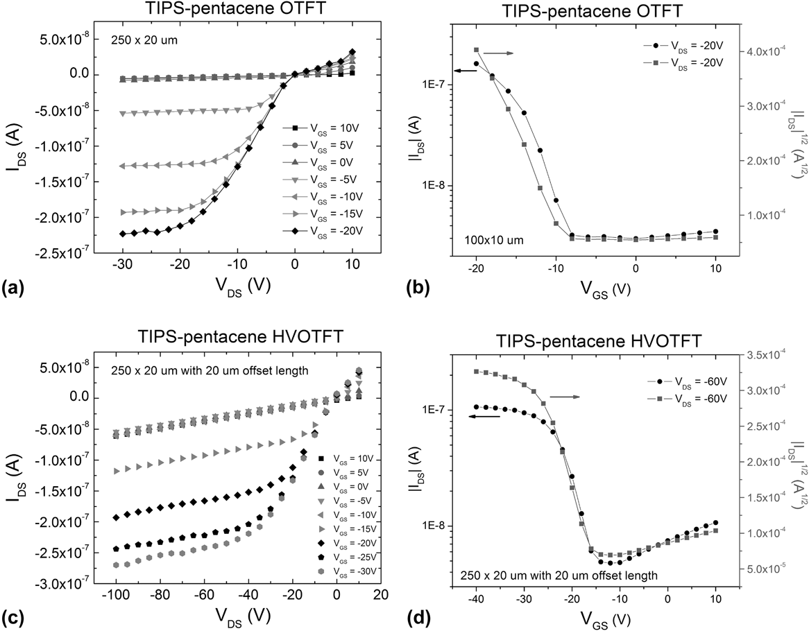
The output and transfer characteristics of the TIPS-pentacene OTFT and HVOTFT are shown in Fig. 2. A large variation in the electrical characteristics from one device to another was observed due to the semi-random crystal orientation inherent from the drop-casting process. However, much care was taken to characterize devices within the same area to minimize variability. Mobility was extracted using the following MOSFET saturation model:
 $$- {I_{{\rm{D}},{\rm{sat}}}} = {{{{\mu _{{\rm{sat}}}} \cdot W \cdot {\varepsilon _0} \cdot \kappa } / {\left( {2 \cdot L \cdot {t_{{\rm{ins}}}}} \right) \cdot \left( {{V_{{\rm{GS}}}} - {V_{\rm{T}}}} \right)}}^2}\quad ,$$
 $${\mu _{{\rm{sat}}}} = {{{m^2}_{{\rm{sat}}} \cdot 2 \cdot L \cdot {t_{{\rm{ins}}}}} / {\left( {W \cdot {\varepsilon _0} \cdot \kappa } \right)\quad ,}}$$
where I D,sat is the drain current, μsat is the saturation mobility, W is the channel width, L is the channel length, t ins is the dielectric thickness, ε0·κ is the dielectric constant, V GS is the gate to source voltage, V T is the threshold voltage, and m sat is the slope of the square root of the drain current versus the gate to source voltage.
(a) Output and (b) transfer characteristics of TIPS-pentacene OTFT. (c) Output and (d) transfer characteristics of TIPS-pentacene HVOTFT.

The mobility of the TIPS-pentacene OTFT with a PFDT SAM coating was 0.0180 cm2/(V s) while that of the HVOTFT was 0.0008 cm2/(V s). The threshold voltage was calculated via a linear extrapolation model and found to be ∼ −1.9 V and −6.8 V for the OTFT and HVOTFT, respectively. Typical I on/I off ratios were found to be on the order of 2 × 10² and 1 × 10² for the OTFT and HVOTFT, respectively. Although the maximum applied bias across the source and drain was relatively low, an increase in the breakdown voltage from −40 to −150 V was observed with the addition of the offset channel region of 30 μm relative to the 20 μm gated channel region. This demonstrates the ability to increase the breakdown voltage by dropping a large portion of the potential across the offset channel region. Nonsaturating electrical characteristics were also observed, particularly for the TIPS-pentacene HVOTFT. This is largely attributed to a space-charge limited current (SCLC) enhanced by the Frenkel effect Reference Smith, Gowers, Shih and Akinwande22,Reference Wang, Fine, Basu and Dodabalapur23 or other short channel effects such as channel length modulation or self-heating. The high-voltage applied across the source and drain contacts induces a strong electric field (0.1–1 MV/cm) such that short channel effects could take place. Although the current output and thus power output is relatively low, it is possible that further increases in mobility could lead to significant self-heating effects which could cause the output current to increase with V DS.
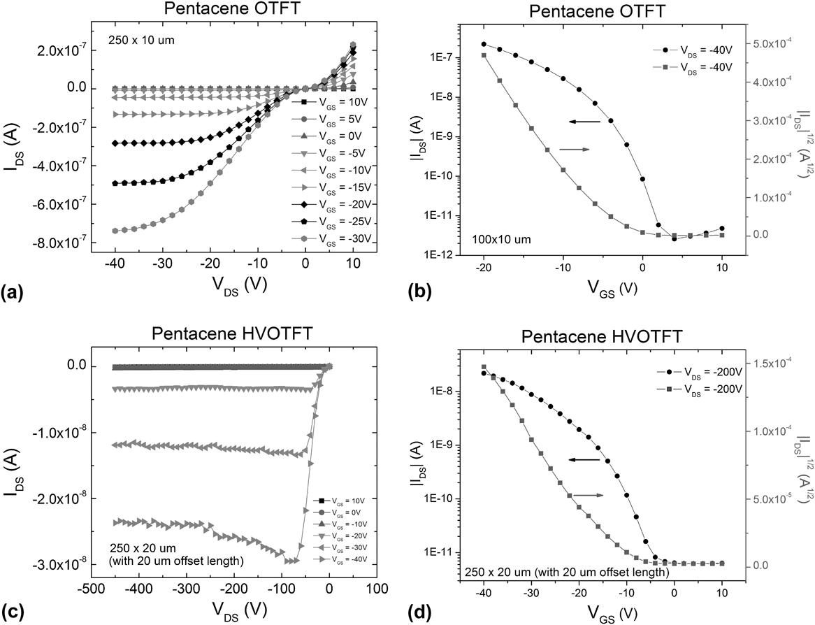
Electrical measurements were also performed on the pentacene OTFT and HVOTFT, shown in Fig. 3. The I–V characteristics were well behaved between pentacene devices as the semiconductor channel is well defined in thickness and surface area. Mobility was found to be 0.0063 cm2/(V s) and 0.0002 cm2/(V s) for the OTFT and HVOTFT, respectively. The threshold voltage shifted negatively, going from −4 to −6.5 V with the addition of the offset channel region. Finally, the I on/I off was measured to be 1.8 × 10⁶ and 3.2 × 10³ for the OTFT and HVOTFT, respectively. Most importantly, however, the breakdown voltage was significantly increased with the added 30 μm offset channel region relative to a 20 μm gated channel region. The breakdown voltage went from ∼ −100 to −550 V. Furthermore, the output I–V characteristics were well behaved with saturating output currents. This is attributed to a more robust fabrication process as well as potential interface states at the dielectric/semiconductor interface which can help reduce the SCLC. Reference Wang, Fine, Basu and Dodabalapur23
(a) Output and (b) transfer characteristics of pentacene OTFT. (c) Output and (d) transfer characteristics of pentacene HVOTFT.

B. Comparing performances between the OTFT and HVOTFT
Comparing both the TIPS-pentacene and pentacene organic semiconductors, the pentacene devices showed significantly higher current I on/I off ratios and breakdown voltages, but with lower mobilities. These results can be explained by the differences in their device designs. There is a lack of transistor isolation as well as a nonuniform and thick (0.5–1.5 μm) semiconductor channel for TIPS-pentacene devices. Furthermore, multiple overlapping crystal grains were usually grown over the channel region, creating line defects. Without proper definition of the semiconductor channel, the devices are susceptible to large leakage currents in the bulk of the organic semiconductor. It is believed that if there is transistor isolation as well as thin TIPS-pentacene layers (below 100 nm), improved current I on/I off ratio and breakdown voltages can be obtained. Nonetheless, higher mobility was achieved with TIPS-pentacene devices and is attributed to the poly-crystalline nature of the organic semiconductor versus the amorphous pentacene. A higher mobility in TIPS-pentacene is expected due to its higher packing density and orbital overlap. Currently, our tilted drop-casting method grows semi-random oriented crystal grains along the direction of the slant. Further work is needed to improve the crystallinity as well as its orientation. It has been suggested in other works that the orientation of the a and b triclinic crystal axis of TIPS-pentacene relative to the transistor channel can be optimized to dramatically increase the charge carrier mobility. Reference Wade, Steiner, Niedzialek, James, Jung, Yun, Bradley, Nelson and Kim24
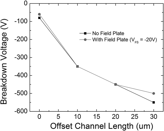
The addition of the offset channel region in the HVOTFT has shown to be effective in increasing the max V DS allowed before breakdown occurs. In fact, increasing the offset channel region length from 10 to 30 μm proved effective in even further increasing the breakdown voltage, as shown in Fig. 4. Apart from increasing the breakdown voltage, the offset channel region reduces the current I on/I off ratio and mobility while making the threshold voltage and the onset to conduction shift to more negative values.
The breakdown voltage acts as a function of the offset channel length for pentacene TFTs. Increased offset channel lengths allows the HVOTFT to handle larger V DS.

I on/I off ratios are reduced in HVOTFTs compared to OTFTs due to a lack of charge carrier control within the organic semiconductor layer. It is plausible that the drain to source bias is largely affecting how and where the hole carriers appear. In the standard OTFT, the bottom gate contact accumulates a thin layer of hole charges at the interface with the dielectric. However, for HVOTFTs, the drain to source bias can introduce charge carriers within the bulk of the organic semiconductor, where there is no gate contact. This, in summary, can lead to detrimental leakage paths and an increased I off current.
Overall, the mobility of the HVOTFTs compared to OTFTs was one to two orders of magnitude smaller. This is attributed to the fact that the offset region acts as a limiting resistor and impedes charge mobility as well as charge injection throughout the channel. Potential multiple gate designs can help introduce more charges within the channel while maintain high-voltage capabilities.
Threshold voltages tended to become more negative with the addition of the offset channel region. Previous work has shown that O2 plasma-treated PAR-C introduced interface traps (Q it), effectively positively shifting the threshold voltage. Reference Smith, Gowers, Shih and Akinwande22 In this case, however, the addition of the offset channel region created a longer channel region that required an additional gate to source biasing to accumulate charges along the entire interface between the organic semiconductor and dielectric.
The onset to conduction, defined as the value of V DS needed to begin achieving high output current I D, was shifted negatively not only when the offset channel region was present but also particularly when V DS was increased beyond −100 V. Typical onset to conduction values shifted from V DS = −1 to −15 V after being subjected to a high drain to source bias, regardless of the gate to source bias. The delayed onset to conduction is indicative of increased charge injection barriers, most likely occurring in the organic semiconductor near the transition between the gated and offset channel regions. Large electric fields originating at the transition region may induce trap-like states, effectively impeding charge injection.
C. Improved charge injection via surface assembled monolayer coating
It has been shown previously that surface assembled monolayers (SAMs) are effective in improving the charge injection from the metal contacts into the organic semiconductor layer. Reference Kim, Meihui, Battaglini, Lang and Horowitz25 Efficient charge injection is primarily limited by the energy barrier height at the interface between the metal contact and the organic semiconductor. Energy barrier height engineering can be achieved by depositing a SAM onto the metal contact which alters the value of the metal work function φM. The length of the SAM molecule and the direction of its dipole moment affect how charge injection is varied. Reference Kim, Meihui, Battaglini, Lang and Horowitz25 Specifically, the hole barrier height is increased when the dipole moment points from the metal to the semiconductor. Likewise, the hole barrier height is decreased when the dipole moment points from the semiconductor to the metal. Previous reports have documented an increase in mobility of pentacene (HOMO level of φHOMO = 4.9 eV) field effect transistors with fluorinated thiolphenols coating the Au contacts (dipole moment pointing from the semiconductor to the metal) and a decrease in mobility with nonfluorinated thiolphenols coating Au contacts (dipole moment pointing from the metal to the semiconductor). Reference Kim, Meihui, Battaglini, Lang and Horowitz25
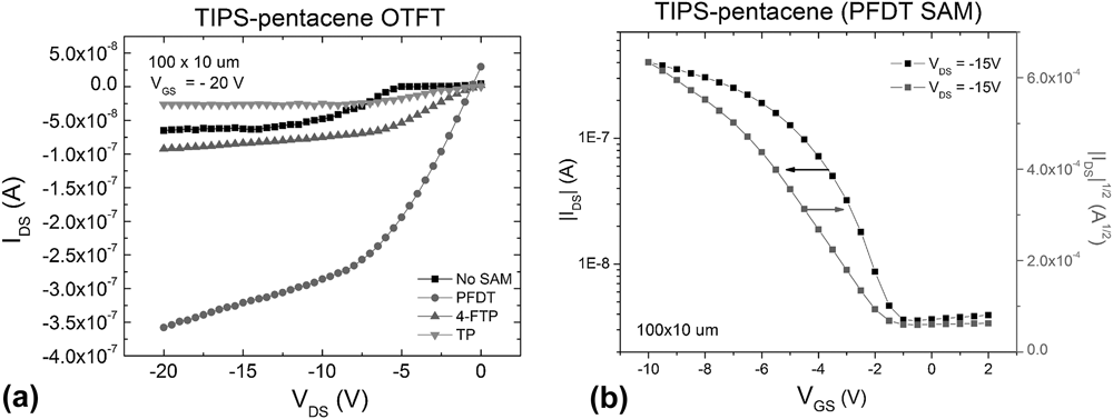
Here, we have deposited one of three types of SAMs on the source and drain Au contacts of our TIPS-pentacene OTFTs. Au has a work function of φAu = 4.6 eV while TIPS-pentacene has a HOMO level of φHOMO = 5.3 eV. This results in a hole injection barrier of ∼0.7 eV. Reference Kim, Meihui, Battaglini, Lang and Horowitz25,Reference Marmon, Battaglini, Lang, Horowitz, Hwang, Kahn, Amato and Calas26 The SAMs used are thiolphenol (TP), 4-fluorothiophenol (4-FTP), and 1H,1H,2H,2H-perfluorodecanethiol (PFDT). The effects of the SAMs were observed by measuring the output characteristics of the devices and comparing them to those of a nontreated sample, as shown in Fig. 5. The main observation made from the electrical measurements is that the current output has increased significantly for devices treated with PFDT compared to nontreated samples. Particularly, PFDT samples showed an increase of mobility by an order of magnitude, going from 0.005 cm2/(V s) for nontreated samples to 0.018 cm2/(V s). The increased charge mobility is attributed to the increased work function of the PFDT coated Au by 0.9 eV. Reference Marmon, Battaglini, Lang, Horowitz, Hwang, Kahn, Amato and Calas26 4-FTP samples also showed a slight increase in mobility up to 0.008 cm2/(V s). TP-treated samples, on the other hand, exhibited a significant decrease in the current output, with its mobility decreasing to 0.0016 cm2/(V s). This is in agreement with the charge injection barrier model.
(a) Output and (b) transfer characteristic of TIPS-pentacene OTFTs made with different SAMs coatings on the metal source and drain contacts. It is shown that the addition of PFDT, a fluorinated thiolphenol, increased the output current and mobility by one order of magnitude.

D. Flexible OTFTs and HVOTFTs
In taking closer steps toward a truly ubiquitous electronic world, HVOTFTs need to be fabricated on arbitrary and flexible substrates. This would enable the ability to drive large voltages, supplying energy to flexible devices for potential micro- and macro-scale actuation. Our previous work reported a flexible pentacene-based HVOTFT with minimal changes to the I–V characteristics. Here, we report a flexible TIPS-pentacene HVOTFT fabricated on a Kapton polyimide substrate.
C–V measurements were first performed to assess the reliability of the BZN and PAR-C individually under flexure. Cross capacitors of area between 400 and 2500 μm2 were measured, and the dielectric constant k was extracted using:
 $$C = {{k \cdot {\varepsilon _0} \cdot A} / d}\quad ,$$
 $$k = {{C \cdot d} / {\left( {A \cdot {\varepsilon _0}} \right)}}\quad .$$
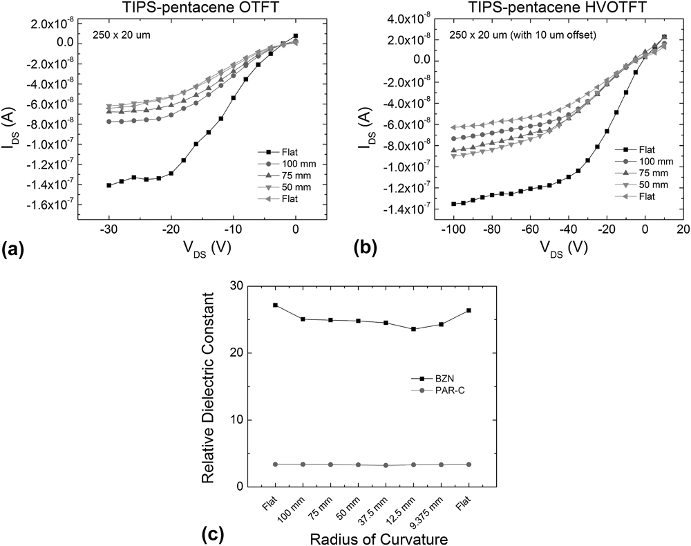
As shown in Fig. 6(c), the dielectric constant decreased marginally during flexure; however, upon relaxation, the dielectric was able to recover. Minimal to no delamination of the dielectric layers was observed.
(a) Output characteristics of a flexible TIPS-pentacene OTFT under various flexure. (b) Output characteristics of a flexible TIPS-pentacene HVOTFT under various flexure. (c) The dielectric constant for PAR-C and BZN remains relatively constant under flexure.

Electrical measurements were performed on the TIPS-pentacene HVOTFTs, progressing from a flat sample to a gradually more curved sample. Radii curvatures used are 8, 6, and 4 inches. The sample was then brought back to a flat configuration for comparison. Flexure was performed parallel to the channel length. As seen from Figs. 6(a) and 6(b), the overall current output and mobility decreased with subsequent bending of the sample. For OTFT devices, mobility decreased, initially sharply and then gradually from ∼6 × 10⁻⁴ to 3.8 × 10⁻⁴ cm2/(V s) while the threshold voltage became more positive, shifting from ∼ −3 to −1 V. For HVOTFT devices, the trend was similar. Mobility decreased from ∼2 × 10⁻⁴ to 1 × 10⁻⁴ while the threshold voltage became more positive, going from ∼ −5 to −3 V. Although not perceivable by optical micrographs, it is believed that microcracks perpendicular to the bending direction, and thus the channel length, are being induced during flexure, which would reduce the overall mobility. Such defects would also act as trap carriers, allowing for intermediate states to hold charges, potentially reducing the threshold voltage. Moreover, the adhesion of the thick TIPS-pentacene to the patterned substrate appeared to be slightly compromised with each bending of the sample. It is believed that adhesion can be improved with a more uniform and thin layer of TIPS-pentacene.
E. Field plate analysis
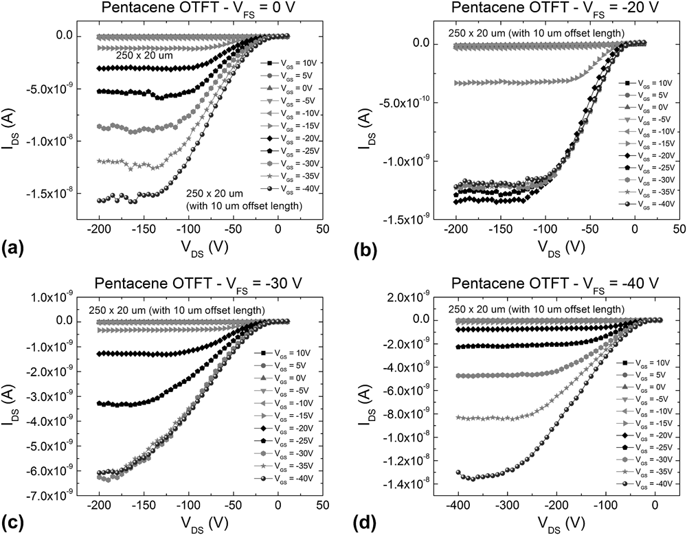
The effects of an additional field plate along with the bottom gate were studied. The top field plate with a length of 5–20 μm parallel to the channel was aligned to be overlapping the transition area between the offset and gated channel regions. The idea behind the field plate was to, one, help populate trap states created by the large stress bias and improve the onset to conduction and, two, to help reduce the large electric field peak that occurs at the channel transition region by introducing an oppositely directed electric field. It has been suggested that the large electric field peak present at the transition region is the cause for dielectric breakdown in the HVOTFTs. Reference Shaw, Hack and Martin28,Reference Martin, Yap, Hack and Tuan29 Due to the solubility of TIPS-pentacene with most solvents as well as its nonuniform surface inherent to drop-casting, only pentacene-based HVOTFTs were fabricated with a field plate. Output characteristics for the HVOTFTs with field plates were initially measured with the field plate floating and then shorted to the source contact. The presence of the field plate in such states did not appear to have any significant effect on the transistor behavior, which was comparable to those of transistors made without field plates. However, when the field plate was subsequently biased, the conductivity of the channel was primarily determined by the field plate to the source potential V FS and not by the bottom gate to the source potential. At a positive V FS, the entire channel was turned off, regardless of the V GS. At a negative V FS, the conductivity of the channel could be controlled by V GS up until the equivalent value of V FS. Additional gate to source biasing beyond that of the field plate to the source did not increase the current output. In other words, V FS dictated the highest conductivity of the channel and acted as a current limiter, as seen in Fig. 7. The effects of the field plate were also reversible in that returning the field plate back to a floating state or to any intermediate bias value brought back the original output characteristics of the transistor. However, with continuing stress via increased V DS, there was a delayed onset to conduction and an overall lower current output. This is again explained by stress-induced trap states at the transition between gated and offset regions, preventing charge injection from the offset to gated channel regions. Further measurements are needed to assess if such stress-induced conductivity changes are reversible or not.
Output characteristics of pentacene-based HVOTFTs with field plates biased at (a) V FS = 0 V, (b) V FS = −20 V, (c) V FS = −30 V, and (d) V FS = −40 V. The field plate potential limits the output current to the equivalent V GS value even if V GS is biased more negatively than the field plate. Changes to the onset of conduction in V DS were also observed with subsequent measurements due to the increasing stress applied.

The breakdown was also assessed for HVOTFTs with fabricated field plates. The field plate to source potential was held at −20 or −40 V, while the gate to source potential was varied between +10 and −40 V at −10 V intervals. V DS was swept from +10 to increasingly more negative values until the breakdown occurred. Interestingly, when −40 V was applied to V FS, the breakdown voltage was generally lower (more positive) by 100–200 V than that of HVOTFTs without field plates. With the field plate biased at −20 V, however, breakdown voltages were comparable. Samples after breakdown were observed under an optical microscope. It appeared that the origin of the breakdown was primarily along the edge of the field plate and the offset region. This suggests that, one, the electric field peak within the channel was not reduced in an effective manner and that, two, a secondary electric field peak was generated between the field-plated region and the offset channel region, inducing another source for breakdown. Other device design configurations are potentially needed to help mitigate such an electrical breakdown. A secondary gate design was also used, in which this gate sat at the bottom of the structure and near the drain side. In such a case, a triple channel region was formed between the source and drain: a gated region, an offset region, and a secondary gated region. The secondary gate was implemented to help introduce additional charges and to increase the current output; however, large potential differences between the drain contact and the secondary gate resulted in an early breakdown well below the values of the single-gated HVOTFT.
Although currently no field plates have been made with TIPS-pentacene devices, a combination of thinner and smoother TIPS-pentacene deposition as well as a shadow mask process will be needed to continue with such device fabrication. Further iterations are needed to improve the breakdown voltage by addition of a field plate.
IV. CONCLUSIONS
We have demonstrated a flexible and solution-processed high-voltage OTFT based off of the organic semiconductor TIPS-pentacene with a breakdown voltage of −150 V. The HOVTFTs and its dielectric layers were also able to sustain their electrical performance under flexure. Such a device could help enable, among others, flexible MEMS applications requiring a wide range of operating voltages for capacitive actuation. We have also shown a well-behaved HVOTFT with vacuum-deposited pentacene that can drive voltages up to −550 V. Although breakdown voltages for the pentacene HVOTFTs are larger than those of the TIPS-pentacene HVOTFTs, further improvements in the crystal growth, thickness uniformity, and device design can help improve the breakdown performance of the TIPS-pentacene devices. Particularly, we believe thinner and patterned TIPS-pentacene will make its electrical performance more reliable as well as comparable to that of the pentacene devices. Nonetheless, TIPS-pentacene devices with a fluorinated thiolphenol (PFDT) SAM coating exhibited much higher mobilities than those of pentacene devices and are promising for making high-output current and high-voltage transistors. We have also shown that the breakdown voltage can be engineered as a function of the offset channel length, to the detriment of I on/I off current ratios. With increased stress on the channel due to a large drain to source bias, charge trap states are created, resulting in impeded charge injection from the offset channel region to the gated channel region. This leads to a delayed onset to conduction. Field plates were designed in the context of reducing the delayed onset to conduction as well as increasing the breakdown voltage. Initial measurements have shown that field plate designs effectively altered the output characteristics of the channel and limited the conductivity to a set value. However, it is yet to be seen if the field plate can help mitigate early breakdown by reducing the electric field peak within the channel. Further field plate investigation is needed.
ACKNOWLEDGMENTS
The authors would like to thank Dr. Melissa Smith and Dr. Annie Wang for their great insight and guidance in the project, Kurt Broderick, Dennis Ward, and Gary Riggott for all their technical assistance and training done at the Microsystems Technology Laboratories, Whitney Rochelle Hess for her help setting up the surface-assembled monolayer experiment and keeping the lab safe, as well as Dr. Charlie Settens and the Center for Materials Science and Engineering for their assistance in XRD measurements.