I. INTRODUCTION AND HISTORY OF PIEZORESISTANCE
To properly understand how and why the electrical resistance of solids changes with the applied mechanical stress, and to fully understand just how different the apparent effects in nanostructures are compared to the bulk case, it is useful to begin by considering the simple undergraduate formula for the resistance:
 $$R = \rho {l \over A}\quad ,$$
where ρ is the resistivity, l is the length, and A is the surface area of a parallelepiped conductor. If this conductor is subject, for example, to a uniaxial tensile stress parallel to its length axis, then the length will increase to l + Δl, whereas the surface area will be reduced because of Poisson's effect from A = w 2 to (w − v∆l)2, where v is Poisson's ratio. In the limit of small strains,  $\varepsilon = {{\Delta l} \mathord{\left/ {\vphantom {{\Delta l} l}} \right. \kern-\nulldelimiterspace} l} \,\,\lt \lt\, 1$, the resulting relative resistance change because of the modified sample dimensions is approximately
 $(1 + 2v){{\Delta l} \mathord{\left/ {\vphantom {{\Delta l} l}} \right. \kern-\nulldelimiterspace} l}$. This yields a measure of the piezoresistance (PZR) called the gage factor, the relative resistance change per unit strain, given by
 $$G = {{\Delta R} \over R}{1 \over \varepsilon } \approx 1 + 2v\quad .$$
For most solids, 0.3 < v < 0.5 so that the geometric PZR is typically expected to lie in the range 1.6 < G < 2. In reality, this range corresponds to the minimum possible gage factor because ρ itself also changes with the applied mechanical stress. Strictly speaking, the PZR is defined as the change in ρ with the applied stress. A more physical definition of the PZR which does not depend on the sample dimensions is the π-coefficient, defined with respect to the applied stress (X) as
 $$\pi = {{\Delta \rho } \over \rho }{1 \over X}\quad .$$
When the geometric changes to a conductor because of the applied stress are negligible, the π-coefficient of Eq. (4) is related to G in Eq. (2) through Young's modulus, Y, because (at least in scalar form) X = Yε.
At the beginning of the 20th century, the observation of a resistance change over and above the geometric change described above was difficult to explain. The fact that ρ varies with the applied stress is not predicted from Drude's classical model of electron motion. In this case, the momentum relaxation time associated with the carrier mobility, τm, varies because of the applied pressure as the inverse of the charge carrier density—in the case of electrons, denoted n. As such the resistivity,
 $$\rho = {1 \over {n{\mu _{\rm{n}}}q}} = {{m^*} \over {n{q^2}{\tau _{\rm{m}}}}}\quad ,$$
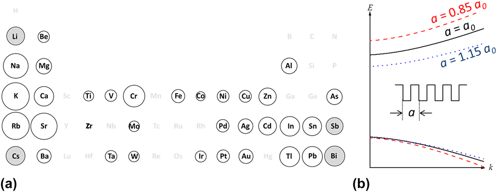
no longer changes with stress (or in the case of the earliest measurement, hydrostatic pressure). Here, q is the absolute value of the electronic charge. Although the first measurements date back well into the 19th century, Bridgman was the first to systematically study PZR in a large selection of metals subject to hydrostatic pressure.Reference Bridgman1 He found PZR coefficients ranging from slightly less than 1 × 10⁻¹¹ Pa−1 (in some of the transition metals), up to about 70 × 10−11 Pa−1 (in the alkali metals). Here, the modern sign convention is followed: compressive stresses are negative, whereas tensile stresses are positive. A positive PZR coefficient under hydrostatic pressure (i.e., a negative stress) implies that for the majority of elements shown in white circles in Fig. 1(a), the resistance drops with the increasing pressure. Figure 1(a) summarizes Bridgman's complete works on the measured pressure coefficients of resistance (for pressures <1 GPa) across the periodic table.Reference Bridgman2 For each element in this figure, the radius of the circle around each symbol is proportional to the decimal logarithm of the measured PZR coefficient (i.e., log10π) so that, for example, the piezoresponse of sodium under hydrostatic pressure is a factor of 10 larger than that of paladium. The clear-cut tendencies across the rows (and within the columns) of the periodic table demonstrate that the PZR is an electronic structure phenomenon. Interestingly, some metals such as bismuth, antimony, lithium, and cesium, compounds of which are currently of interest for their unusual electronic properties,Reference Fu, Kane and Mele3 exhibit anomalous behavior where the resistance increases with pressure (shaded gray circles). A correct explanation of PZR phenomena, therefore, requires a quantum mechanical description. (Bridgman motivates his work by suggesting that the limitations of Drude's classical description of electron motion, and the need for a different (quantum) theory, would have been revealed earlier if more attention had been paid to measurements of resistance under pressure dating from the second half of the 19th century. Instead, a definitive demonstration of this had to wait until the more difficult measurement of the specific heat of solids at low temperatures in the early 20th century.)
(a) A graphical representation of the measured piezoresistance (PZR) coefficients (here under hydrostatic pressure) of a large number of metallic elements (from Refs. Reference Bridgman1 and Reference Bridgman2). The radius of the circle around each element is proportional to the logarithm of the measured coefficient. Unshaded circles correspond to the usual negative coefficients (i.e., a reduction in resistance with increasing pressure), whereas the gray-shaded circles correspond to anomalous increases in resistance with increasing pressure. Grayed-out elements correspond to materials that were not measured. The trends across the rows (and in the columns) of the periodic table demonstrate that PZR is an electronic structure phenomenon requiring a quantum mechanical description. (b) The effect of applied mechanical stress on electronic structure demonstrated by plotting the dispersion relations obtained from the one-dimensional Kronig–Penney model. With respect to the nominal zero stress case (solid black line), 15% tensile strained (dotted blue line), and 15% compressive strained (dashed red line) cases exhibit a stress-induced change in the band gap, the effective masses, and the density-of-states. According to Eq. (4), each of these changes can, in principle, contribute to a stress dependence of the resistivity, ρ.

Armed with the tools of quantum mechanics, it is immediately clear from even the simplest one-dimensional models of the crystal potential that mechanical stress should modify ρ. Consider the Kronig–Penney model in which a non-interacting electron moves in a periodic one-dimensional array of square potential wells spaced by the lattice parameter, a = a 0. The potential wells represent the atoms of the one-dimensional lattice. As is well known, an analytical solution to Schrodinger's equation exists in this case, and the dispersion relationship between energy, E, and wavevector k, is given byReference Wolfe4
 $$\cos (ka) = \cos \left( {\alpha a} \right) + {m \over {\hbar^2 \alpha }}\sin \left( {\alpha a} \right)\quad ,$$
where  $\alpha ^2 = 2mE/ \hbar^2$ and m is the free electron mass. A band gap in the electronic structure described by Eq. (6) is shown in Fig. 1(b) (black solid curve). If a is now reduced from its initial, unstressed value (a 0) to 0.85a 0 to simulate a compressive stress resulting in a 15% strain, the dispersion relations are modified according to the dashed red lines in Fig. 1(b). This figure also shows (dotted blue lines) the effect of an increase of a to 1.15a 0 of its initial value which simulates an applied tensile stress resulting in 15% strain. The dependence of Eq. (6) on a results in a band gap dependence on stress, an effective mass dependence on stress, and also a dependence of the density of states,
 $2\pi g = {{dk} \mathord{\left/ {\vphantom {{dk} {dE}}} \right. \kern-\nulldelimiterspace} {dE}}$, on stress. It is then clear that the mobility μn = μn(X) depends on the applied stress because of the change in both the effective mass and in the momentum relaxation time,
 $\tau _{\rm{m}} \propto {1 \mathord{\left/ {\vphantom {1 g}} \right. \kern-\nulldelimiterspace} g}$, with stress. Moreover, the carrier concentration also becomes stress-dependent, n = n(X), through its dependence on g and on the band gap. Thus, even ignoring changes to the electron dynamics induced by stress, it is clear that
 $${\rm{\rho = \rho }}\left( X \right) = {1 \over {n\left( X \right){{\rm{\mu }}_{\rm{n}}}\left( X \right)q}}\quad .$$
II. PZR IN BULK SILICON
Perhaps the most extreme, non-Drude-like case considered by Bridgman was that of the crystalline semiconductors, germanium and silicon.Reference Bridgman2 Even a qualitative description of the observed behavior was difficult because “the resistance is susceptible to dislocations” and the “non-hydrostatic nature of the pressure,” that is, the crystalline nature of the material. Although he was unable to draw any concrete conclusions regarding the properties of these materials, he did note that, in the case of silicon, the sign of the π-coefficient changed depending on whether the crystal was doped n-type or p-type. In fact, these observations came only 2 years before the classic experimental work of Smith that revealed the PZR effect in germanium and silicon in qualitative detail.Reference Smith5 The results obtained by Smith were particularly striking in that, for silicon under the appropriate conditions, the measured π-coefficients were more than twice as large as those measured in the alkaline metals potassium and rubidium [see Fig. 1(a)], although they were found to decrease with increases in the doping density sufficiently large to push the semiconductor into the degenerate regime.Reference Tufte and Stelzer6
Smith suspended small weights from monocrystalline boules of silicon and germanium. By doing this for a variety of crystal orientations and for current flow either parallel or perpendicular to the applied, uniaxial tensile stress, he was able to estimate the π-coefficients for all configurations and to show that, in general, it is a tensor quantity.Reference Smith5 He also showed, like Bridgman, that the dopant type significantly modifies the PZR. Although he offered only a phenomenological description of the effect, the microscopic description of the phenomenon in n-type silicon, where the electronic structure is relatively simple, was rapidly accomplished.Reference Herring and Vogt7 To understand this co-called charge-transfer model, it is useful to consider the case of a uniaxial compressive stress applied along the <100> direction in bulk n-type silicon. The longitudinal PZR (i.e., when an electrical current is flowed parallel to the direction of the applied stress) will be considered.
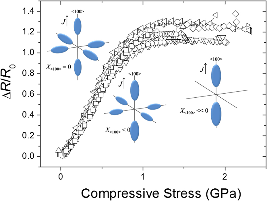
Under zero applied stress, the conduction band minima of silicon are approximately 83% of the distance to the Brillouin zone boundary along the ΓX or {100} crystal directions. Consequently, the iso-energetic surfaces are no longer spheres but degenerate ellipsoids of which there are six. These ellipsoids are characterized by two effective masses; the parallel and transverse effective masses that correspond to the major and minor axes of the ellipsoids, respectively. When a compressive uniaxial stress is applied along the <100> direction, the ellipsoids with the long axis oriented along the <100> direction (i.e., the longitudinal ellipsoids) are shifted down in energy with respect to the ellipsoids whose long axis is oriented parallel to the <010> and <001> crystal directions (i.e., the transverse ellipsoids). Electrons from the perpendicular valleys are then transferred to the parallel valleys so that the density-of-states effective mass changes. Because the parallel mass is larger than the transverse mass, according to Eq. (5) a measurement of the resistance along the <100> direction reveals an increase in its value with increasing applied compressive stress. This increase continues until all the electrons are transferred from the transverse to the longitudinal valleysReference Aubrey, Gubler, Henningsen and Koenig8 as indicated in Fig. 2. This has recently been verified up to unprecedentedly high stresses of the order of 3 GPa.Reference Milne, Favorskiy, Rowe, Arscott and Renner9 With respect to Eq. (3), therefore, the PZR in n-type silicon is primarily because of a change in the m* and thus the mobility, μn, of conduction band electrons. Based on this description, the PZR is quite clearly dependent on crystal direction, and a qualitative description of the effect in all directions can be obtained using Smith'sReference Smith5 treatment and the method described by Kanda.Reference Kanda10
Longitudinal piezoresistance in n-type silicon along the <100> crystal direction (Adapted from Ref. Reference Milne, Favorskiy, Rowe, Arscott and Renner9). At zero applied stress, the conduction band minimum consists of six equivalent valleys along the <100> directions that are degenerate and therefore equally populated. As the uniaxial compressive stress is increased, the degeneracy of the six valleys is lifted. The longitudinal valleys shift downwards in energy relative to the four transverse valleys resulting in a charge transfer to the two longitudinal valleys. This changes the density-of-states weighted effective mass because the parallel and perpendicular masses are not equal. Because the parallel mass is greater than the transverse mass, this increases the resistance until all the charge is transferred from the transverse valleys. The diagrams (inset) schematize the charge transfer process.

The valence band structure is more complex, with three bands in close (energetic) proximity near the band maximum at the center of the Brillouin zone. It was recognized early on that the charge transfer mechanism would therefore not describe the PZR in p-type silicon.Reference Adams11 In the intervening period between Smith's first measurements and the beginning of the 21st century, a number of authors have treated and tried to identify the key elements that describe PZR in p-type silicon.Reference Ohmura12–Reference Richter, Pedersen, Brandbyge, Thomsen and Hansen15 In addition to charge transfer between, for example, heavy- and light-hole bands, their proximity also results in a band warping (i.e., a change in the curvature of each band as stress is applied) and potentially to changes in τm because of stress-induced modifications in the scattering rates. Surprisingly, for a material whose electronic properties have been studied in detail since the 1950s, the preponderance of each of these effects is still to some extent debated, leading for example to conflicting predictions about the PZR at high stress.Reference Thompson, Sun, Choi and Nishida16,Reference Fan, Register, Winstead, Foisy, Chen, Zheng, Ghosh and Banerjee17 In the simplest band-edge models, the PZR was predicted to saturate at high stress much like the n-type case,Reference Thompson, Sun, Choi and Nishida16 whereas solutions of the Boltzmann equation using the full band structure predict a much weaker, or even an absence of saturation, at least up to 4 GPa.Reference Fan, Register, Winstead, Foisy, Chen, Zheng, Ghosh and Banerjee17 Recent experimental results along with ab initio band structure calculations demonstrate that the latter interpretation is probably correct.Reference Milne, Favorskiy, Rowe, Arscott and Renner9 The details of the longitudinal PZR along the <110> and the <111> crystal directions are of interest, not only to engineers exploiting strained silicon technology to increase the hole mobilityReference Thompson, Sun, Choi and Nishida16 but also because these are the most common orientations of silicon nanowires where the largest PZR is claimed.Reference He and Yang18
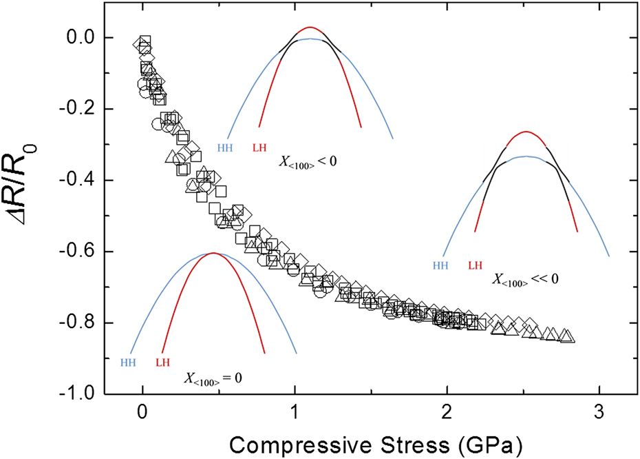
Under a compressive uniaxial stress applied parallel to the <110> crystal direction, the light-hole band (LH) moves to higher energies, whereas the heavy-hole (HH) band moves down. This is shown schematically in the inset of Fig. 3. In doing so a band anticrossing appears, initially near the Brillouin zone center and moving outwards as the stress increases. This anticrossing is extremely important for the PZR because the effective mass of holes in states near the anticrossing is significantly different from either that of the heavy or the light holes. As the stress increases, the anticrossing moves out to higher wavevectors and into the tail of the hole distribution.Reference Milne, Favorskiy, Rowe, Arscott and Renner9 Below stresses of approximately 3 GPa, there is still a non-negligible population of holes near this band anticrossing and this results in very little drop off in the resistance change with the applied stress in this range (Fig. 3). The case of an applied stress along the <111> crystal direction is qualitatively similar to the <110> case. In general therefore, the PZR in p-type silicon, like the n-type case, is because of a change in the transport effective mass.
Longitudinal piezoresistance (PZR) in p-type silicon along the <110> crystal direction (Adapted from Ref. Reference Milne, Favorskiy, Rowe, Arscott and Renner9). At zero applied stress, the HH and LH bands are degenerate at the Brillouin zone center. As the uniaxial compressive stress is increased, this degeneracy is lifted, with the LH (red) band moving upwards in energy relative to the HH (blue) band. The resulting anticrossing (black) yields a significant fraction of holes whose transport effective mass is very different from either the HH or the LH mass. The population of holes near this anticrossing, which moves to lower energies further from the center of the Brillouin zone with increasing stress, is still non-negligible at room temperature and at stresses near 3 GPa. Saturation of the PZR is therefore weak or nonexistent. At higher stresses, all the holes will reside in the top band and have an effective mass given by the LH mass. In the absence of any stress-induced changes in τm, the PZR is then expected to saturate.

A largely overlooked point, which may be important for the understanding of the PZR of nanowires, is the nonlinearity in the PZR response for both n-type and p-type silicon. Although the form and values of higher order PZR coefficients have been described and measured, the aim has usually been to address nonlinearities at higher stress levels (i.e., in the 100 MPa range and above).Reference Matsuda, Kanda, Yamamura and Suzuki19,Reference Matsuda, Suzuki, Yamamura and Kanda20 In fact, it is clear from the above discussion that the first order PZR coefficients should not be the same in compression and in tension. In the n-type case treated above, compressive stress corresponds to the transfer of electrons from the four transverse valleys to the two longitudinal valleys. Naturally, tensile stress will result in a transfer of electrons from the two longitudinal valleys to the four transverse valleys. The resulting variations in resistance with therefore be different in compression and in tension. Similarly, for p-type silicon in the case treated above, compressive uniaxial stress shifts the LH band upwards resulting in the band anticrossing. Eventually, all holes will reside in the warped LH band. In tension, the reverse occurs, and the HH band moves upwards in energy. There is no band anticrossing, and eventually all holes reside in the HH band. Like n-type material, the stress response is asymmetric. As a result, the π-coefficients can be significantly different when measured in compression or in tension. For example, recent measurements of the π-coefficients in compressionReference Milne, Favorskiy, Rowe, Arscott and Renner9,Reference Shifren, Wang, Matagne, Obradovic, Auth, Cea, Ghani, He, Hoffman, Kotlyar, Ma, Mistry, Nagisetty, Shaheed, Stettler, Weber and Giles21,Reference Tsang, O’Neill, Gallacher and Olsen22 are up to a factor of 2 larger than Smith's values in p-type material and almost half of those obtained by Smith for n-type material. Full band ab initio calculations from large compressive stress to large tensile stress support these experimental conclusions.Reference Kozlovskiy and Sharan23
III. GIANT PZR IN SILICON NANOSTRUCTURES
In semiconductor nanostructures that are sufficiently small, there can be a significant change in the electronic structure because of the quantum confinement. Given that the PZR in bulk material is closely related to the electronic structure, it is natural that it may also be modified by quantum confinement. The first experimental indication of this is the early work of Dorda in the surface inversion layer of bulk silicon.Reference Dorda24,Reference Dorda25 At low temperatures, the PZR along particular crystal directions is found to be much larger than that of bulk silicon with gage factors up to 1500. Both charge transfer and a stress-induced scattering mechanism resulting in a strongly stress-dependent τm in Eq. (5) have been invoked to describe these observations.Reference Eisele26,Reference Dorda, Eisele and Gesch27 Quantum confinement leads to even more impressive, low temperature resistance changes in n-type AlAs quantum wells. In this case, a two-dimensional version of the charge transfer mechanism yields extraordinarily large gage factors up to 50,000.Reference Shkolnikov, Vakili, De Poortere and Shayegan28 In p-type material, distortion of the hole band dispersion relationships results in similarly large gage factors.Reference Habib, Shabani, De Poortere, Shayegan and Winkler29
Unlike these reports, there are as yet no experimental studies of PZR in semiconductor nanowires of sufficiently small diameter that quantum confinement begins to play a role. Work on silicon nanowires started with Yasutada et al.Reference Yasutada, Toriyama and Sugiyama30, who studied the effect of applied stress first on polycrystalline nanowires and then on top-down fabricated single crystal nanowires.Reference Toriyama, Tanimoto and Sugiyama31,Reference Toriyama, Funai and Sugiyama32 Although these authors report gage factors up to 50% larger than the results of SmithReference Tufte and Stelzer6 in nanowires of approximately 50 nm diameter, there is nothing to suggest that the observed PZR is anything other than the known bulk phenomenon, particularly given the reported variationsReference Beaty, Jaeger, Suhling, Johnson and Butler33 in measured π-coefficients in bulk silicon. Moreover, the applied stress was only roughly estimated using ex situ finite element calculations of the nanowire geometry, which may result in significant errors. The work which reignited interest in PZR in semiconductors was the report of giant PZR (GPZR) in bottom-up grown silicon nanowires in 2006.Reference He and Yang18
In the bottom-up grown single crystal <111> oriented silicon nanowires subjected to both compressive and tensile stress, longitudinal π-coefficients up to 100 times larger than those of bulk silicon were reported.Reference He and Yang18 Not only is the PZR extremely large but it is also strongly nonlinear, with a large change of resistance per unit applied stress occurring for compressive stress rather than tensile stress, reminiscent of bulk silicon PZR when studied at large stresses.Reference Milne, Favorskiy, Rowe, Arscott and Renner9,Reference Shifren, Wang, Matagne, Obradovic, Auth, Cea, Ghani, He, Hoffman, Kotlyar, Ma, Mistry, Nagisetty, Shaheed, Stettler, Weber and Giles21–Reference Kozlovskiy and Sharan23 Several proposed explanations of the PZR phenomenon are based on quantum effects in atomically thin nanowires.Reference Cao, Gong and Wu34–Reference Niquet, Delerue and Krzeminski38 In one case at least,Reference Cao, Gong and Wu34 an interplay between the HH and LH electronic structure of the surface atomic layer and the interior atoms of the nanowire results in a predicted PZR behavior that strongly resembles the data of He and Yang.Reference Kleimann, Semmache, Le Berre and Barbier14 In other calculations, a stress-induced shift from an indirect to a direct band gap is predicted to yield a large sudden change in the resistance at several percent strain.Reference Shiri, Kong, Buin and Anantram35,Reference Leu, Svizhenko and Cho37 However, in some reports at small strains, the calculated deformation potentials (i.e., the amount by which the electronic bands move per unit strain) in nanowires are very similar to those of bulk silicon.Reference Aubrey, Gubler, Henningsen and Koenig8,Reference Milne, Favorskiy, Rowe, Arscott and Renner9,Reference Leu, Svizhenko and Cho37 In these cases, the characteristic length scale for the predicted phenomena is the quantum, or de Broglie, wave length. In silicon at 300 K, this is typically of the order of 1 nm, which is much smaller than the diameters of the experimentally tested nanowires (which vary from approximately 50 nm up to 300 nm). As such, the nanowire diameters are too large for the GPZR to be any type of quantum size effect like those observed in surface accumulation layers or quantum wells.Reference Dorda24–Reference Habib, Shabani, De Poortere, Shayegan and Winkler29 These first principle calculations are therefore of interest for potential future PZR experiments on radially quantum confined nanowiresReference Canham39 with diameters below approximately 2.2 nm.Reference Zhao, Wei, Yang and Chou40 In He and Yang's relatively large nanowires, one therefore expects the electronic structure to be that of the bulk material, and it is for this reason that the apparent GPZR is such a surprising, unexpected, and interesting result.
Although He and YangReference He and Yang18 did not attempt to describe the microscopic details of the PZR they observed, they naturally suspected that the surface had some role to play. It was shown, for example, that both the nanowire resistance and PZR depend strongly on surface chemical treatments; both are reduced when the nanowires are hydrogen passivated using a hydrofluoric acid etch. Reoxidation using nitric acid makes both parameters increase. Moreover, by studying the gate voltage dependence of the PZR, they concluded that the GPZR was linked primarily to a change in the charge carrier mobility (and not the concentration), similar to the bulk PZR. A key realization concerning a possible origin for the GPZR effect came afterward, when the correlation between partial depletion of the nanowire and GPZR was made.Reference Rowe41
By comparing the nanowire diameters with the characteristic electrostatic penetration depth—the surface depletion layer width—it was noticed that GPZR apparently occurs only in nanowires where the diameter is comparable to or smaller than the surface depletion layer width. When this is the case, the density of free charge carriers in the nanowire becomes sensitive to the charge state of the surface. For small enough diameters, the free carrier density within the conducting nanowire channel is entirely determined by the surface charge state. If this surface charge can be modified by an applied stress, then a large change in carrier density (and hence conductivity) will result. This would at least qualitatively explain the sensitivity of the observed phenomena to surface chemical modification, but is at odds with He and Yang's claim that a mobility change is the principal origin of the GPZR. Despite this difference, the so-called piezopinch modelReference Rowe41 in which a stress-induced change of the surface charge density is modeled by a shift in the surface Fermi-level pinning, qualitatively describes the observed PZR as a function of nanowire diameter and doping level very well.Reference Rowe41,Reference Nghiem, Aubry-Fortuna, Chassat, Bosseboeuf and Dollfus42 The only parameter in this model is the degree by which the surface Fermi-level shifts with the applied stress, dE F/dX. To match the He and Yang's observations, dE F/dX ≈0.5 meV/MPa is found.Reference Rowe41 This is intriguingly close to stress-induced changes in trap activation energy measured in metal-oxide-silicon capacitors,Reference Hamada and Takeda43 which lends some weight to the piezopinch idea. Unlike either the quantum mechanical confinement effects, or in the bulk effect, where the PZR is principally the result of a stress-induced change in the charge carrier mobility, the piezopinch model predicts a PZR based on a change in the charge carrier concentration. [A stress-induced change in the charge carrier concentration is also invoked to describe the PZR of silicon nanoneedles under biaxial stress (see Ref. Reference Xiao, She, Deng and Xu44), although in this case a piezopinch description is not used.] This is consistent with the known effects of surface state doping of nanowires.Reference Kumar Bhaskar, Pardoen, Passi and Raskin45 He and Yang's data, therefore, tentatively support an electrostatic interpretation of the GPZR whose characteristic length scale can be as large as several micrometers at low doping densities. Having said this, if the basic piezopinch idea is correct, the microscopic origin of the surface Fermi-level shift is yet to be identified.
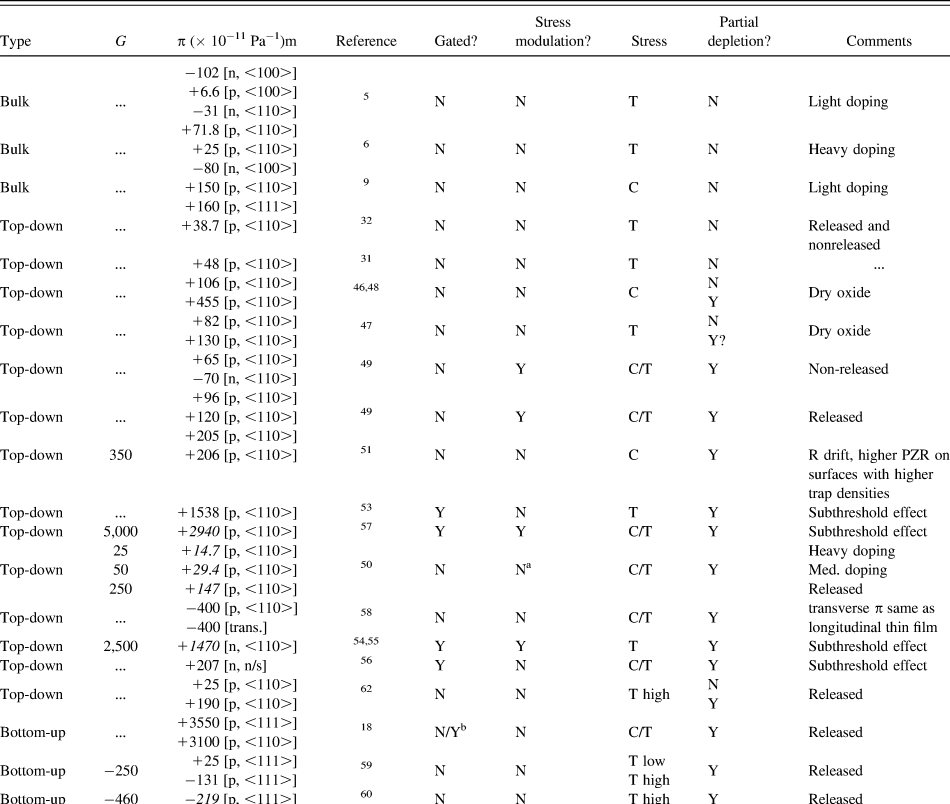
At approximately the same time the piezopinch idea was developed, other authors had also noticed the fact that the apparent GPZR depends strongly on the doping density.Reference Reck, Richter, Hansen and Thomsen46 This early experimental work on top-down fabricated nanowires also reports large π-coefficients with a reduction in doping density for nanowires of fixed diameter, although the values are not quite as large as those given by He and Yang. To test the piezopinch and quantum confinement models, and to further explore the PZR in silicon nanowires, a number of groups subsequently undertook experimental work on top-down fabricated nanowiresReference Reck, Richter, Hansen and Thomsen46–Reference Barwicz, Klein, Koester and Hamann51 in subthreshold nanowire transistor channelsReference Rochette, Cassé, Mouis, Haziot, Pioger, Ghibaudo and Boulanger52–Reference Neuzil, Wong and Reboud57 and in silicon thin films.Reference Milne, Rowe, Arscott and Renner49,Reference Yang and Li58 With some exceptions,Reference Lugstein, Steinmair, Steiger, Kosina and Bertagnolli59,Reference Zhang, Liu, Ru, Zhang, Dong and Sun60 very little subsequent work has been performed on bottom-up grown nanowires. Table I summarizes the measured gage factors and longitudinal π-coefficients along with the accepted values for bulk silicon and those reported in Ref. Reference He and Yang18. From the table, it is clear that the literature contains both claims and counter-claims of GPZR, and these will be discussed below.
Summary of longitudinal π-coefficients and gage factors (G) reported in bulk and nanostructured silicon. In cases where only G is given, the Young's modulus for the given crystal directionReference Wortman and Evans61 is used to calculate the π-coefficient (these values being given in italics).

a Resistance variations are carefully monitored as a function of time.
b In He and Yang's work, the gated nanowires are also tested with the aim of determining whether the PZR is because of a mobility or concentration change. The effect on the PZR of placing the transistor structure in the subthreshold regime is not specifically discussed.
Reported results are obtained during periods where the zero-stress resistance does not vary significantly with time.
A. Effect of electrostatic depletion
Electrostatic depletion in nanowires or thin films is obtained in ungated structures by reducing the doping concentration (which in the most commonly used p-type material is denoted N A), so that the surface depletion layer width
 $$W = \sqrt {{{2\varepsilon {\phi _{\rm{b}}}} \over {q{N_{\rm{A}}}}}} \quad ,$$
increases to the point where it is comparable to (or larger than) the smallest dimension of the nanowire or thin film, L. Here, ε is the dielectric constant of the material, q is the absolute value of the electronic charge, and  ${\phi _{\rm{b}}}$ is the surface potential barrier resulting from the presence of charge trapping in localized surface states.Reference Vu, Arscott, Peytavit, Ramdani, Gil, André, Bansropun, Gérard, Rowe and Paget63 The actual value of
 ${\phi _{\rm{b}}}$ depends on the microscopic details of the surface states themselves, the doping in the bulk of the semiconductor and the crystal orientation of the surface.Reference Himpsel, Hollinger and Pollak64 In silicon, it can vary over more than 0.7 eV relative to the bulk position of the Fermi level.Reference Terman65–Reference Wagner and Spicer67 This will clearly affect the critical doping density at which W ∼ L. It is reasonable, however, for an order-of-magnitude estimate of the depletion of nanowires and thin films, and to simplify the following discussion, to assume that the
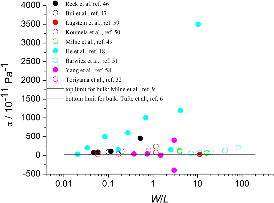
 ${\phi _{\rm{b}}}$ = 0.55 eV, that is, the surface Fermi level is pinned in the middle of the band gap. In the cases where partial depletion is induced by reducing the doping density (and not by depleting a transistor channel with a gate voltage), an estimation of W is made in this way for the literature summarized in Table I. Figure 4 shows a plot of the reported longitudinal π-coefficients versus the ratio W/L.
Summary of measured longitudinal π-coefficients in p-type silicon nanowires and thin films as a function of carrier depletion as measured by the ratio W/L (see text). The higher the value of W/L, the more the structure is depleted of free charge carriers. The horizontal black lines represent minimum and maximum experimentally measured values in bulk p-type silicon.

This figure is particularly informative concerning the state of the art in silicon nanowire PZR. The two horizontal black lines represent typical minimum and maximum values of the bulk p-type longitudinal π-coefficients. Although there are crystal directions for which the PZR response is zero,Reference Kanda10 the minimum value taken here is that measured in highly doped material along the <110> direction.Reference Fu, Kane and Mele3 The maximum value is that obtained under compression in lightly doped material along the same crystal direction.Reference Milne, Favorskiy, Rowe, Arscott and Renner9 Although not all measured nanowires are orientated with their long axes along the <110> direction, for the majority this is the case. A striking feature of Fig. 4 is the relative lack of reports of GPZR with π-coefficients significantly outside the accepted range of reported bulk values. Apart from the report of He and YangReference He and Yang18, the only other claims of significantly larger PZR are those of Reck et al.,Reference Reck, Richter, Hansen and Thomsen46,Reference Reck, Richter, Hansen and Thomsen48 and Yang and Li.Reference Yang and Li58 Koumela et al.Reference Koumela, Mercier, Dupré, Jourdan, Marcoux, Ollier, Purcell and Duraffourg50 report values of slightly above the acceptable bulk range.
The work of ReckReference Reck, Richter, Hansen and Thomsen46 is intriguing because not only does it report large PZR, but (as mentioned above) it also explores the variation in PZR with doping density. It is clear from Fig. 4 that these authors measure a progressive increase in the longitudinal π-coefficient with increasing W/L. Although this is the tendency that is expected based on quantum degeneracy arguments in bulk silicon,Reference Kanda10 the maximum values that are measured seem to be significantly larger than the largest reported values in bulk silicon. Contrast this with another interesting work on nanowires where the surface crystal orientation is found to affect the PZR.Reference Barwicz, Klein, Koester and Hamann51 In this case, the same tendency with a change in doping density is observed, but the measured π-coefficients fall much closer to the known range of bulk values (see also Fig. 4). It is therefore tempting to suggest that the result reported by Reck is evidence of a phenomenon different to that of bulk silicon, and one might tentatively conclude that a piezopinch descriptionReference Rowe41,Reference Nghiem, Aubry-Fortuna, Chassat, Bosseboeuf and Dollfus42 would suitably describe the data. Indeed, the π-coefficient values shown in Fig. 4 and in Table I are not far from those of He and YangReference He and Yang18 for equivalent W/L ratios.
Another report of GPZR is that of Yang and Li in very thin silicon films.Reference Yang and Li58 In this case, the authors go to some length to point out that a quantum mechanical confinement effect is not the cause of the observed effect, and that a large effect is observable only for the thinnest films where W/L >> 1. Along the lines of the piezopinch model, they suggest that the explanation for the GPZR is a stress-induced change in the surface charge density. They make two intriguing experimental claims: (i) that the longitudinal PZR coefficient is large and identical (in magnitude and sign) to the transverse coefficient. This clearly indicates that if the PZR effect is real, it is not a bulk electronic structure effect and (ii) that the longitudinal π-coefficient changes sign with a change from tensile to compressive applied stress, that is, regardless of the sign of the applied stress, the resistance always decreases [see Fig. 3(c) in Ref. Reference Yang and Li58]. The second of these claims is rather difficult to justify in terms of a real PZR effect. An even response as a function of stress suggests that the Fermi energy at zero stress sits exactly on a degenerate pair of identical states whose stress response (shift in energy, change in curvature, etc.) is exactly equal and opposite. There are no known silicon surface states that possess this property.Reference Himpsel, Hollinger and Pollak64–Reference Chadi, Citrin, Park, Adler, Marcus and Gossman66 A more likely explanation for the observed resistance change is simply a non-stress-related surface charge relaxation.Reference Milne, Rowe, Arscott and Renner49,Reference Anderås, Vestling, Olsson and Katardjiev68 With reference to Fig. 3(c) in Ref. Reference Yang and Li58, it is likely that the true PZR is the slight difference in the slopes of the curves for tensile and compressive applied stress. This is possibly just the bulk silicon PZR.
This charging effect, or dielectric relaxation, was first revealed in nanowires in the study by Milne et al.,Reference Milne, Rowe, Arscott and Renner49 where the true PZR of a large set of top-down nanowires was found to be comparable to that of bulk silicon. Milne went further to suggest that the non-stress-related surface charging effects, which only show up in partially depleted structures, might well lead to claims of apparent GPZR. Although the work of Yang and LiReference Yang and Li58 seems to fall into this category, the question with respect to the data shown in Fig. 4 is whether the work of He and Yang,Reference He and Yang18 or indeed Reck's,Reference Reck, Richter, Hansen and Thomsen46,Reference Reck, Richter, Hansen and Thomsen48 does as well. The work of He on the effect of surface functionalization on nanowire resistance and PZR clearly shows that the observed phenomena are sensitive to surface charge, but there is no outright published evidence that the reported resistance changes are because of anything other than the applied stress. This is of course far from being proof that the large resistance changes are because of the applied stress. The same is true for the work of Reck. Without further investigation, it is difficult to argue either for the unambiguous existence of GPZR in nanowires or for clear signs of dielectric relaxation. Having said this, Milne et al.Reference Milne, Rowe, Arscott and Renner49 showed that it is simple to design a time-modulated stress experiment on samples like He's or Reck's that would greatly clarify the interpretation of these two early reports of GPZR. Although this technique has been used by several authors who investigate gated or transistor-like nanowires,Reference Kang54,Reference Kang55,Reference Neuzil, Wong and Reboud57 it has not been widely used in ungated (i.e., air exposed) nanostructures.
In their work, Koumela et al.Reference Koumela, Mercier, Dupré, Jourdan, Marcoux, Ollier, Purcell and Duraffourg50 were careful to monitor resistances as a function of time to avoid any possible misinterpretation. They pursued a slightly different route to others and chose to investigate the effect of releasing the nanowires from the buried oxide (BOX). Their observations suggest that releasing nanowires systematically increases the π-coefficient. For example, a nanowire with a boron doping density of 2 × 1020 cm−3 (W/L ∼ 0.06) has a measured longitudinal π-coefficient of approximately 25 × 10−11 Pa−1 in good agreement with bulk material.Reference Fu, Kane and Mele3 When the 145 nm thick BOX is removed this increases to approximately 60 × 10−11 Pa−1, almost a factor of 3 increase. Similarly, a less-doped nanowire (5 × 1017 cm−3, W/L ∼ 1.2) sees its π-coefficient increase from 70 × 10−11 to 240 × 10−11 Pa−1, a boost of just over 3. It seems unlikely that the nature of the surface oxide has changed during the release process—both before and afterward it is just the native oxide.However, the actual diameter of the silicon nanowire itself is probably slightly reduced from its pre-release value because of the etch process. This would thereby increase W/L and perhaps lead to an increase in the π-coefficient according to the piezopinch model.Reference Rowe41 Another possibility is a stress concentration effectReference Pilkey69,Reference Bashir, Gupta, Neudeck, McElfresh and Gomez70 because of the geometry of the released nanostructure. In this case, the real stress along the length of the nanowire may be significantly larger than the externally applied stress with the measured resistance change being simply because of the bulk silicon PZR. It is also interesting to note that Milne et al.Reference Milne, Rowe, Arscott and Renner49 measured boosts in π-coefficients up to a factor of two in nanowires upon their release (and without any other change in the nanowire itself). Such a stress concentration phenomenon may affect, to a lesser extent, unreleased nanowires.
The final important feature of Fig. 4 that should be discussed is the relative lack of work performed on bottom-up grown nanowires—in this figure, there are only two examples, that of He and YangReference He and Yang18 and the work of Lugstein et al.Reference Lugstein, Steinmair, Steiger, Kosina and Bertagnolli59 The results of Lugstein are rather different to those of He and Yang, with only small π-coefficients being measured despite very strong depletion of the nanowires. Intriguingly, Lugstein uses the stress modulation techniqueReference Milne, Rowe, Arscott and Renner49 to avoid resistance drifts that might be interpreted as a GPZR effect. At high stresses in the GPa range, the π-coefficients of these <111> oriented change sign, and this observation has been confirmed elsewhere.Reference Zhang, Liu, Ru, Zhang, Dong and Sun60 This in contrast with the work of Kumar Bhaskar et al.Reference Kumar Bhaskar, Pardoen, Passi and Raskin62 on <110> oriented top-down nanowires at GPa stresses where the π-coefficients do not change sign. Although the results on bottom-up grown nanowires are therefore inconsistent, the fact that the biggest values in Fig. 4 are claimed in this type of wire may not be without merit. Having said this, if there is a significant difference between bottom-up and top-down fabricated material, it is yet to be identified, although it is possible to speculate on a number of potentially important differences.
First, because the phenomena seem to be related to surface states, the fact that bottom-up wires have facetted surfaces may be important, as this is known to affect the surface state distribution.Reference Himpsel, Hollinger and Pollak64 This might differentiate the properties of He and Yang's nanowires, which have facets normal to the {211} crystal directions, from Lugstein's nanowires that have {111} oriented surface facets. Depending on the exact microscopic details of the atomic configurations associated with a particular trap state, the state's energy may be stress dependentReference Hamada and Takeda43 or not. Second, bottom-up grown nanowires are known to contain significant quantities of the catalytic metal, usually gold, in the body of the nanowires and on the surface.Reference Hannon, Kodambaka, Ross and Tromp71 Given that gold is known to form deep charge traps in silicon,Reference Lang, Grimmeiss, Meijer and Jaros72 if the activation energy of these localized states is found to be stress-dependent, they might be responsible for a piezopinch effect in partially depleted, bottom-up nanowires that would be absent in top-down nanowires. Another potentially important point is the surface roughness of the nanowire, which tends to be greater in dry-etched top-down structures. Reck et al.Reference Reck, Richter, Hansen and Thomsen46 point out that surface roughness scattering could conceivably quench any piezoresistive effect, including the bulk one. In this picture, even if GPZR exists in top-down nanowires, it may be quenched by this scattering process.
B. Gated or transistor-like nanowires
Table I tells a rather different story in gated or transistors-like nanowires in which a gate potential can be used to place the transistor in its subthreshold regime. In this case, there are several claims of GPZR with π-coefficients well above the bulk range as indicated in Fig. 4. These will be individually examined in this section.
The first such work is that of Passi et al.,Reference Passi, Ravaux, Dubois and Raskin53 who find that the longitudinal π-coefficient varies from an acceptable bulk value in the linear response region of the transfer curve up to 1600 × 10−11 Pa−1 in the subthreshold region. Although the stress-modulation method is not used, the reproducibility of the results as a function of gate bias for several different applied stresses suggests that there is no dielectric relaxation causing resistance drift.Reference Milne, Rowe, Arscott and Renner49,Reference Anderås, Vestling, Olsson and Katardjiev68 Subsequent work has usually attempted to address this possible shortcoming directly by implementing some form of dynamically applied stress.Reference Kang54–Reference Neuzil, Wong and Reboud57 In all of these cases, GPZR in the subthreshold region is observed, with the largest claimed valuesReference Neuzil, Wong and Reboud57 approaching those measured by He and YangReference He and Yang18 on ungated bottom-up nanowires.
In Neuzil's case,Reference Neuzil, Wong and Reboud57 the geometry of the sample is rather unusual, with two parallel nanowires connected electrically in series. Moreover, the wires are placed in a moveable cantilever that is actuated to apply stress. The gate is the fixed substrate itself. An unusual feature of the transfer curves of the nanowires is the subthreshold slope (i.e., dI DS/dV G), which is approximately 160 mV/decade. This is comparable with the best performance of recently developed tri-gate, 22-nm node devices fabricated by Intel,Reference Auth, Allen, Blattner and Bergstrom73 which is rather surprising for a relatively large unoptimized device structure in which the gate electrode is some distance from the conducting nanowire channel itself. This behavior suggests that there is some geometric boost to the effective gating effect that may itself be of interest. One possibility might be the close proximity of the two parallel nanowires that yields some electrostatic coupling between the two. Whether this apparently very large sub-threshold slope has an effect on the PZR is not clear, but the electrical behavior of this sample geometry is clearly more complex than a single isolated, gated nanowire geometry.
Such criticism cannot be leveled at Singh et al.'s,Reference Singh, Park, Miao, Shao, Krishna Kotlanka and Kwong56 and in particular at Kang's work.Reference Kang54,Reference Kang55 In these cases, the subthreshold slopes are much more modest as would be expected for devices of this size. Like the work of Passi et al.,Reference Passi, Ravaux, Dubois and Raskin53 very large clear-cut changes in the nanowire resistance under applied stress are observed in the subthreshold region. In these cases, the GPZR seems, therefore, to be reproducible, and the question is then: why are gated structures so different from ungated ones where there is as yet no convincingly repeated evidence of GPZR?
The fact that the GPZR occurs only in the subthreshold region of gated structures certainly suggests an electrostatic origin for the effect, that is, a stress-induced effective gating of the nanowire channel. Two possibilities present themselves—either a stress-driven effect where the applied stress modifies the density of trapped charge in the gate oxide, or a strain-driven effect where the applied stress modifies the distance between the gate electrode and the nanowire channel. The first of these is just the piezopinch effect,Reference Rowe41 and it closely resembles early device ideas in which the gate oxide of transistors is replaced with a piezoelectric dielectric to render the transistor highly sensitive to applied stress.Reference Greeneich and Muller74 In this case, gage factors up to 7000 are observed. It is, however, difficult to understand why a piezopinch mechanism would not also be clearly present in ungated oxidized nanowires. The second possibility seems unlikely given that in the majority of works,Reference Passi, Ravaux, Dubois and Raskin53–Reference Singh, Park, Miao, Shao, Krishna Kotlanka and Kwong56 the subthreshold slope is not large enough to account for such a large resistance change under such a small resulting strain, that is, the physical motion of the gate electrode relative to the channel because of the applied stress is probably too small or even negligible. Having said this, in a nonuniform object like a gated nanowire, stress concentrationReference Pilkey69,Reference Bashir, Gupta, Neudeck, McElfresh and Gomez70 may result in much larger-than-expected strains so this possibility should not be ruled out without further investigation.
C. Silicon nanowire strain gages
There are a number of publications in the literature whose goal is to use silicon nanowire elements as strain gages for the detection of a variety of microelectromechanical (MEMS) or nanoelectromechanical (NEMS) transduced forces.Reference He, Feng, Roukes and Yang75–Reference Allain, Parrain, Bosseboeuf, Mâaroufi, Coste and Walther80 In some cases,Reference Mile, Jourdan, Bargatin, Labarthe, Marcoux, Andreucci, Hentz, Kharrat, Colinet and Duraffourg76,Reference Allain, Parrain, Bosseboeuf, Mâaroufi, Coste and Walther80 the authors recognize that although GPZR in partially depleted nanowires would be attractive from a force sensitivity viewpoint, the partial depletion leads to very high resistances and to an augmented sensitivity to environmental changes (i.e., humidity, temperature, etc.) resulting in dielectric relaxation.Reference Milne, Rowe, Arscott and Renner49 In the view of these authors, exploitation of any nanowire PZR is, therefore, best achieved by using high doping densities to reduce resistance and surface sensitivity while maintaining a PZR effect based on the known bulk phenomenon at high charge carrier density.Reference Fu, Kane and Mele3,Reference Kanda10 Other articles either directly claimReference He, Feng, Roukes and Yang75 to exploit the GPZR, or simply imply its useReference Zhang, Lou and Lee78 in a selected application. In these works, it is very difficult to determine whether the resulting device sensitivity is a consequence of GPZR, or whether it is simply a combination of bulk silicon PZR and a well-designed detection protocol. As such, they do not add significantly to the discussion of the GPZR effect itself.
Still other nanowire strain gage applications use a gated nanowire geometry.Reference Singh, Miao, Pott, Park and Kwong77,Reference Sansa, Fernandez-Regulez, San Paulo and Perez-Murano79 Given the discussion above in Sec. III. B, in this geometry any increase in sensitivity is potentially the result of GPZR. One caseReference Singh, Miao, Pott, Park and Kwong77 uses the same unusual double-nanowire geometry used by Neuzil et al.,Reference Neuzil, Wong and Reboud57 although ultra-high subthreshold slopes are not reported. This work by Singh et al.Reference Singh, Miao, Pott, Park and Kwong77 is intriguing because it is the only report of both the gate effect and a reduction in doping density on nanowire PZR. Their data support the main observations given in this review—a reduction in doping density increases the π-coefficient, and this increase is much more pronounced when the nanowire transistor is placed in its subthreshold region. The work of Sansa et al.Reference Sansa, Fernandez-Regulez, San Paulo and Perez-Murano79 is also interesting in that it uses a separate gate and nanowire structure that, in principle, permits a stress-induced movement of the gate with respect to the nanowire. As indicated in Sec. III. B, if such a movement occurs when the transistor is in the subthreshold region, the subthreshold slope will determine the magnitude of the PZR.
D. Other potentially important issues
There are several other important issues which could potentially complicate the interpretation of PZR data in nanowires. The two most significant of these are (i) in-built stress within the nanowire, either as grown for bottom-up nanowires, or residual stress in the active layer of the silicon-on-insulator (SOI) films in the case of top-down nanowires and (ii) poorly characterized electrical contacts, in particular to partially depleted bottom-up grown nanowires.
In the case of the residual stress in SOI thin films, the active layer stress resulting from the fabrication procedure has been known for some time.Reference Iida, Itoh, Noguchi and Takano81 Recently, in-built compressive stresses up to more than 300 MPa were found in commercial SOI wafers.Reference Allain, Le Roux, Parrain and Bosseboeuf82 This level of stress is clearly not negligible when compared with the typical external stresses applied to nanowires during PZR measurements which are usually at most approximately 100 MPa. Moreover, because the PZR response of bulk silicon is strongly nonlinear, even around zero applied stress,Reference Milne, Favorskiy, Rowe, Arscott and Renner9,Reference Kozlovskiy and Sharan23 an in-built stress might significantly modify the apparent π-coefficient of top-down nanowires fabricated from SOI wafers, even if the PZR response is nothing more than that of bulk silicon. Similarly, it is entirely possible that the growth of bottom-up grown nanowires between confining side walls,Reference He and Yang18 the evaporation of electrical contacts onto nanowire bridges,Reference Lugstein, Steinmair, Steiger, Kosina and Bertagnolli59 or the use of external probes to measure nanowire resistance,Reference Zhang, Liu, Ru, Zhang, Dong and Sun60 may also result in an uncontrolled offset stress in these materials [Given that the state of the residual stress is not usually characterized, its probable presence justifies the comparison of PZR data under externally applied compressive and tensile loads in Table I despite the expected differences between the two (see Sec. II).]. These issues are potentially important because the PZR response to an external applied stress can depend on the initial stress state of the nanowire.Reference Rochette, Cassé, Mouis, Haziot, Pioger, Ghibaudo and Boulanger52
The lack of knowledge about the electrical properties of the nominally Ohmic contacts to partially depleted nanowires is also problematic. In principal, in top-down nanowires, even partially depleted ones, low-resistance Ohmic contacts can be formed in the contiguous active silicon layer by the usual implantation and metal evaporation techniques.Reference Milne, Rowe, Arscott and Renner49However, in bottom-up grown nanowires, there is not only likely to be a significant quantity of metal catalyst at one or both ends of the nanowire, but the formation of a space charge junction between the lightly doped nanowire and a more heavily doped substrate cannot be ruled out. In this case, it is possible that a rectifying junction is formed at each end of the nanowire so that the overall object's equivalent circuit is given by back-to-back diodes.Reference Chung, Yu and Heath83 This could also influence the PZR properties of the nanowires.Reference Creemer, Fruett, Meijer and French84
IV. CONCLUSIONS AND FUTURE POSSIBLE RESEARCH DIRECTIONS
The literature strongly indicates that GPZR does exist in partially depleted silicon nanowires, but only in structures containing an electrostatic gate plane that biases the nanowire into the subthreshold region. Unambiguous proof of GPZR in ungated structures is lacking, with the majority of works reporting π-coefficients that are conceivably linked to a bulk silicon PZR phenomenon, or that are potentially marred by the effects of dielectric relaxation. A piezopinch (or electrostatic) explanation may be the correct qualitative interpretation for the GPZR in transistor-like structures, but this is incompatible with the absence of a clear effect in ungated nanowires. Possible future research directions to address this issue might include (i) a study of the stress dependence of trap state activation energies in thermal and native oxides, for example, by deep-level transient spectroscopy or by using Kelvin probe microscopy. This might help to address the microscopic origins of an effect based on the piezopinch idea, (ii) an investigation of the effects of the stress distribution in the nanostructures, either with an eye to estimating the effect of stress concentration or to evaluate the possibility of a change in gate/channel distance, (iii) a more thorough understanding of in-built stresses in the nanowires, and (iv) an evaluation of the electrical properties of the contacts, especially in the case of partially depleted, bottom-up nanowires where the possibility for the formation of rectifying junctions at each end of the wire exists.
A second axis for future research concerns the exploration of the PZR properties of bottom-up nanowires. There is very little literature on this type of nanostructure, and given that the biggest π-coefficients are claimed in bottom-up materials more work is certainly justified. Potentially important differences between top-down and bottom-up nanowires could then be explored, for example, a potential role for gold-related trap states in the piezopinch model. The principal challenge in this case is the fabrication of Ohmically contacted nanowires which is significantly more difficult than in the case of top-down nanowires and nanostructures. A third possibility is to push nanowire dimensions down to quantum length scales where a number of interesting phenomena, including GPZR, are theoretically predicted based on ab initio band structure calculations. This is currently a challenge for growers of bottom-up silicon nanowires where easily achievable minimum nanowire diameters are of the order of 30 nm.
GPZR is the basis for an enabling technology for a wide range of force transduction applications which require the sensitive electrical detection of MEMS or NEMS motion. Moreover, mechanical stress is a key ingredient in the semiconductor technology roadmap for the improvement of microelectronic device performance. Aside from the purely scientific goal of understanding the phenomenon, a better understanding of the PZR properties of nanowires and nanowire transistors should therefore be a priority.
ACKNOWLEDGMENTS
This work was supported by the Agence Nationale de la Recherche (PIGE ANR-2010-021). The author thanks S. Arscott for many fruitful discussions and for a critical reading of the manuscript.