

INTRODUCTION
Today nano-material in both particulate and thin films form finds application as functional elements on surfaces, into volumes, and as nano-hybrids viz. in bioactive composites and nano-biomarkers. These nano-particles/thin films prepared by conventional gas phase processes are often agglomerated to micro-powders that are hardly used for functional matrices and chemical methods often lead to impurities of the nano-particle (Abdelsaye et al., Reference Abdelsayed, Glaspell, Nguyen, Howe and El-Shall2008; Hahn et al., Reference Hahn, Barcikowski and Chichkov2008). In the last decade, laser ablation technique has proven to be a unique and efficient technique to generate, excite, fragment, and conjugate elemental, nano-alloy, semiconductor, and ceramic nano-particles (Pavell et al., 2000). Metal nano-particles formed in comparison to the conventional synthesis shows remarkable properties such as a 3–5 times higher number of bio-molecules, which can be conjugated to laser-generated, ligand-free gold/silver nano-particle surface (Hahn et al., Reference Hahn and Barcikowski2009; Hodak et al., Reference Hodak, Henglein and Giersig2000). Besides, pulse laser ablation technique offer advantages for growth of well adhered epitaxial thin film layers of many advanced materials on different substrate with high deposition rates (Rimal et al., Reference Rimal, Ager, Logothetis, Weber and Hangas1991; Capano et al., Reference Capano, Walck, Murray, Dempsey and Grant1994; Taylor et al., Reference Taylor and Atwater1998; Trusso et al., Reference Trusso, Barletta, Barreca, Fazio and Neri2005; Wang et al., Reference Wang, Xu, Zhou, Chu and Fu2007; Hörlein et al., Reference Horlein, Steinke, Henig, Rykovanov, Schnurer, Sokollik, Kiefer, Jung, Yan, Tajima, Hegelich, Nickles, Zept, Tsakiris, Sandner and Habs2011). Studies of interaction of intense laser beam with matter and their plume characterization find applications in generating various grades of metal (Wang et al., Reference Wang, Xu, Zhou, Chu and Fu2007; Fazio et al., Reference Fazio, Neri, Ossi, Santo and Trusso2009), metal oxide (Sukla & Khare, Reference Shukla and Khare2010), carbide and nitride nano-materials generation (Katharia et al., Reference Katharria, Kumar, Prakash, Choudhary, Singh, Phase and Kanjilal2007), thin films formation and other areas (Veiko et al., xxxx). Of these advanced materials, SiC, carbon on Silicon carbide and carbon films all find utmost importance due to their remarkable properties and application.
SiC offers unique properties such as wide band gap energy (2.3–3.2 eV), high thermal conductivity (5–7 Wcm−1 K−1), high breakdown field (>20 × 105 V/cm), high saturation velocity (2.2 × 107 cm/s), high mobility (1000 cm2/Vs), high resistance to oxidation and corrosion, low expansion coefficient, high thermoelectric power, high thermal and chemical stability, higher hardness, and elastic modulus, etc. (Casady et al., Reference Casady and Johnson1996; Tabbal et al., Reference Tabbal, Said, Hannoun and Christidis2007; Keffous et al., Reference Keffous, Bourenane, Kechouane, Gabouze and Kerdja2007; Katharria et al., Reference Katharria, Kumar, Prakash, Choudhary, Singh, Phase and Kanjilal2007; Takao et al., Reference Takao, Kohno, Ichikawa and Takeda2008;). All these properties of SiC make it suitable for different applications such as: pressure sensors (Wu et al., Reference Wu, Zorman and Mehregany2006), hydrogen gas sensors (Fawcett et al., Reference Fawcett, Wolen, Myers, Walker and Saddow2004), fuel atomizer (Rajan et al., Reference Rajan, Zorman, Mehregany, Deanna and Harvey1998), and blue light-emitting diode (Ziegler et al., Reference Ziegler, Lanig, Theis and Weyrich1983), etc. As one of the radiation resistant material, it can also be used for high energy laser and plasma facing nuclear fusion reactor wall materials (Hirohata et al., Reference Hirohata, Koboyashi, Maeda, Nakamaru, Mohri, Watanabe and Yamashina1979). Various methods such as electron beam physical vapor deposition (Zhao et al., Reference Zhao, He, Sun, Yi and Xiao2009), radio-frequency sputtering (Costa et al., Reference Costa, Camargo, Achete and Carius2000), metallic organic chemical vapor deposition (Lim et al., Reference Lim, Jee, Kim, Moon, Lee, Choi and Boo.2004), and pulsed laser deposition (Gusev et al., Reference Gusev, Ryndya, Kargin and Bondarenko2010) have been used to form hard silicon carbide films. Pulse laser deposited metal carbide and nitride and carbon foil of nano-metric thickness find application in generating high harmonic radiation that is a topic of interest now (Hörlein et al., Reference Horlein, Steinke, Henig, Rykovanov, Schnurer, Sokollik, Kiefer, Jung, Yan, Tajima, Hegelich, Nickles, Zept, Tsakiris, Sandner and Habs2011).
Carbon in various forms such as amorphous carbon, graphene, diamond, and carbon nano-tube on SiC (C-SiC) exists with very special properties. C-SiC composite thin film enhances fracture toughness besides the hardness and abrasive properties. High pressures (Ekimov et al., Reference Ekimov, Gavriliuk, Palosz, Gierlotka, Dluzewski, Tatianin, Kluev, Naletov and Presz2000) or powder sintering (Zhao et al., Reference Zhao, Qian, Daeman, Pantea, Zhang, Voronin and Zerda2004; Reference Zhao, He, Sun, Yi and Xiao2009), and indirect plasma heating of β-SiC grains (Nayak et al., Reference Nayak, Behera and Mishra2010), Chlorination of SiC at 1100°C are used for formation of diamond on SiC surface (Welz et al., Reference Welz, Gogotsi and Mc Nallan2003).
Similarly, graphene on SiC surface exhibits remarkable electronics performance such as very high carrier mobility (Stiver, Reference Stiver2009). These carriers with no mass move with constant velocity like photons and as the most promising positive band gap material it finds application as fast communication materials (Siegel et al., Reference Siegel, Zhou, Gabaly, Schmid, Mccarty and Lanzara2009; Reference Siegal, Hwang, Fedorov and Lanzara2010; Presser et al., Reference Presser, Heon and Gogotsi2011; Vizzini et al., Reference Vizzini, Enriquez, Chiang, Oughaddou and Soukiassian2011). Polariton enhanced reflectivity at SiC/graphene interface plays an important role to overcome the diffraction limit of light, especially applicable to nano-photonic devices viz. plasmonic wave-guide (Qazi et al., Reference Qazi, Nomani, Chandrashekhar, Shields, Spencer and Koley2010). Besides formation of packed carbon nano-tubes at the SiC-carbon interface, it is also reported that it does not contribute to carrier mobility. Existence of a multilayer and rotatable graphene layers (observed from moiré pattern) on Si terminated 4H-SiC (0001) has also been reported by Stiver (Reference Stiver2009) (vide infra).
Monolayers of graphene formation by laser annealing of 4H-SiC films under 10 W laser power, 30 kHz frequency with a laser spot velocity of 0.8 cm/s, and argon pressure of 2 Torr has been reported by Perrone et al. (Reference Perron, Maccioni, Chiolerio, Martinez De Marigorta, Naretto, Pandolfi, Martino, Ricciardi, Chiodoni, Celasco, Scaltrito and Ferrero2009). Similarly, Berger et al. (Reference Berger, Song, Li, Wu, Brown, Naud, Mayou, Li, Hass, Marchenkov, Conrad, First and de Heer2006) and Dawlaty et al. (Reference Dawlaty, Shivaraman, Strait, George, Chandrashekhar, Rana, Spencer, Veksler and Chen2008) reported epitaxial graphene synthesis viz. Si sublimation from Si-face of semiconducting 6H and 4H SiC. It involves heating up the SiC substrates in a vacuum at 1200°C to 1600°C.
In this paper, we report an alternate method of formation of graphene on SiC, i.e., by converting amorphous carbon present in the SiC surface to graphene form by bombarding carbon ions onto a C rich SiC films. Pulse laser ablation technique has been used for the same. Detailed characterization data of the resulted film by Fourier transform infrared (FTIR), Micro-Raman, X-ray reflectivity, and emission scanning electron microscopic (FESEM) with nano-indentation were done and the results are discussed.
EXPERIMENTAL
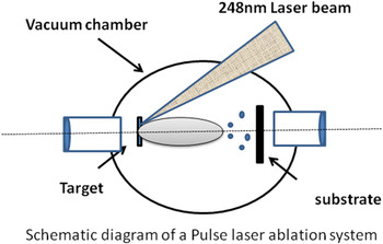
A schematic drawing of the pulse laser ablation setup is shown in Figure 1 and the same was used for deposition of both SiC and carbon thin films. Experiments were carried out in two parts. In the first part, 300 nm thin SiC films were formed by pulse laser deposition with annealing and then on the same further carbon films were deposited. Detail experimental conditions are given below.
Schematic diagram of the pulse laser ablation setup.

SiC films were deposited on Si (100) by pulsed laser deposition setup (M/s. Photonics, Singapore) from a SiC target (stoichiometric, 99.5% purity). A KrF excimer laser (λ = 248 nm, pulse width = 25 ns) was focused to a spot size of 4 mm2 on rotating SiC target at a pulse frequency of 10 Hz and pulse energy of 400 mJ at the laser side, yielding an energy density of about 5 J/cm2 (with 50% loss at the target side). Optically cleaned (using standard Si cleaning procedure) p-type Si (100) wafer with resistivity of 1–10 Ωcm were used as the substrate. Laser light was irradiated and focused at an angle of 45° to the target and the substrate was placed parallel to the target with a provision to heat the same up to 830°C. Target to substrate distance was kept at 4 cm. The chamber pressure was maintained at a vacuum level of 7 × 10⁻⁶ mbar. Substrate temperature at 800°C and deposition time of 30 min were kept fixed for all the experiments. SiC films and graphene rich SiC are denoted as SiC and C-SiC films and were characterized using various physical and chemical methods and the results are described below.
The crystal structure and phase composition of the films were identified by the glancing angle X-ray diffraction (Rigaku, Model: Ultima-IV) method using CuKα radiation with a glancing angle of 1°. Both thickness and roughness of the films were determined by analyzing the X-ray reflectivity data using the global fit software. To identify the bonding between the different elements in the film, FTIR spectra were obtained using a Perkin Elmer model based FTIR system working in the wave number region of 400–4000 cm−1. Raman spectra were carried out by micro-Raman spectrometer (In Via Renishaw, U.K) equipped with confocal microscope with a charge-coupled device camera detector and samples were excited using 514 nm argon laser. Detailed depth analysis of SiC film and C-SiC films were carried out at 30 s exposure at 100% laser power. Micro-structural studies were carried out by field emission scanning electron microscope (Supra 55, Carlzeiss, Germany) at 8 kV. Micrographs were taken in both BSE modes with their cross-sectional images showing the thickness of these films. Elemental distributions of different elements present in the film were done by energy dispersive X-ray spectroscopy analysis. Typical films surfaces were observed under transmission electron microscope (Model JEOL, TEM-2012, UHR) at 200 kV. Here only copper grid without any carbon coating was used.
Elastic modulus and hardness of the films were determined using a nano-indenter (UMIS, Fisher-Cripps, Australia). In nano-indentation, the depth of penetration of a diamond indentor is measured along with the prescribed load. The resulting load-displacement response typically shows an elastic-plastic loading followed by an elastic unloading. The elastic equations of contact are then used in conjunction with the unloading data to determine the elastic modulus and hardness of the specimen materials. A load of 1 mN each at about 10 points was applied on the surface of the films with an interval of 10 µm between each indent. Oliver-Pharr method (Pharr, Reference Pharr1998) was used for evaluation of elastic modulus and hardness of the film. The Poisson's ratio of the SiC films and carbon film was taken to be 0.17. In the text, the laser energy refers to the laser side with 50% loss at the target side.
RESULTS AND DISCUSSIONS
Adherent a C and graphene thin films were formed on SiC thin films. These films were found to be uniform and smooth with very low surface roughness and were characterized in detail using various physical techniques (vide infra). Results of some typical thin films are discussed below.
X-Ray Diffraction Studies
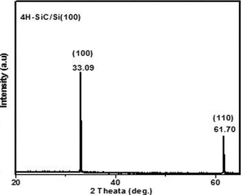
X-ray diffraction data of typical vacuum annealed SiC film showed peaks due to 4H-SiC at 2θ (in degree) = 33.09 and 61.7 pertaining to <100> and <110> crystalline plane (Fig. 2). This result corroborates with the Raman data shown below. X-ray diffraction of the other unannealed SiC and C-SiC thin film sample were amorphous in nature and did not show any useful information.
X-ray diffraction pattern of vacuum annealed SiC film showing peaks due to 4H SiC.

X-Ray Reflectivity Studies
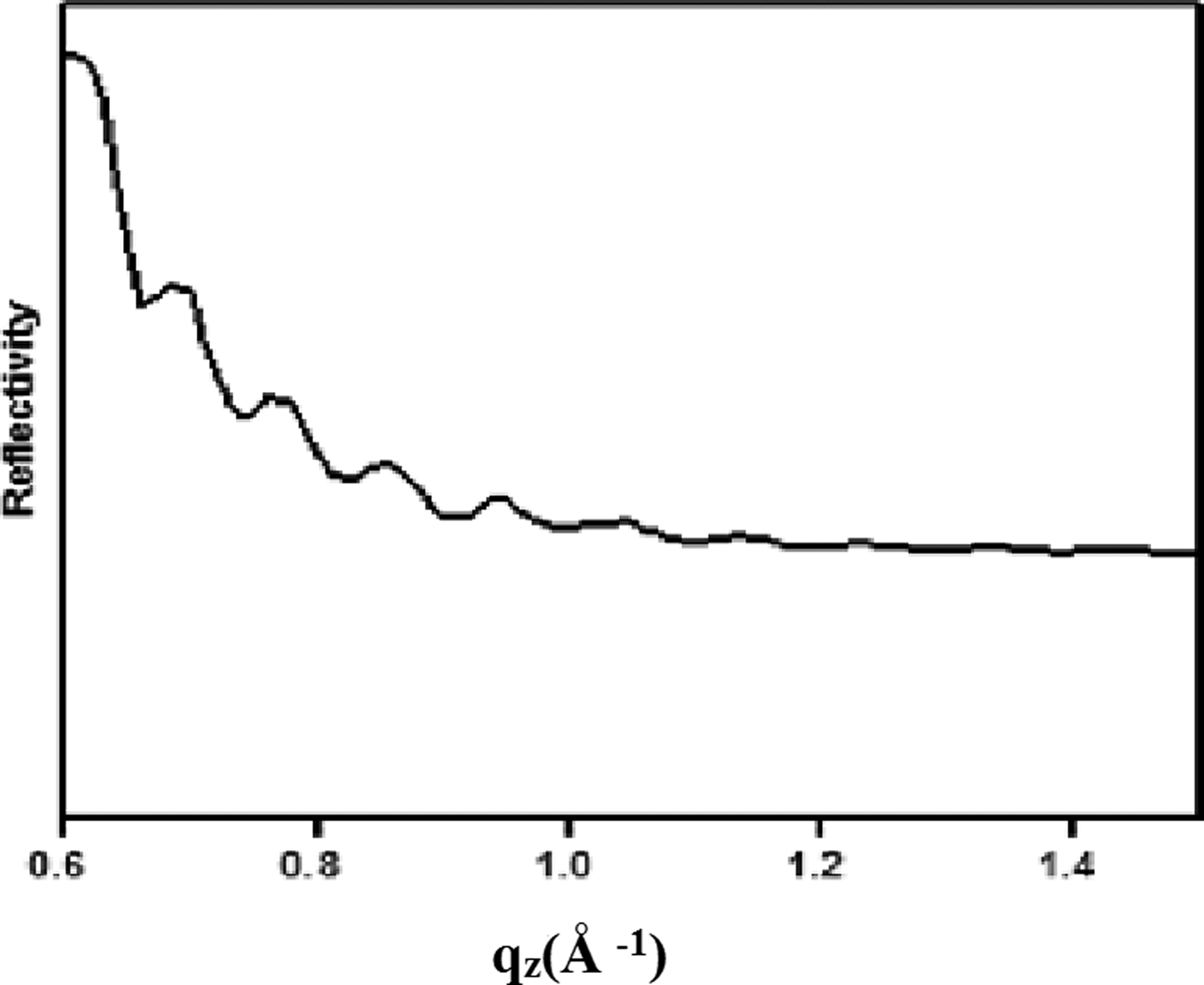
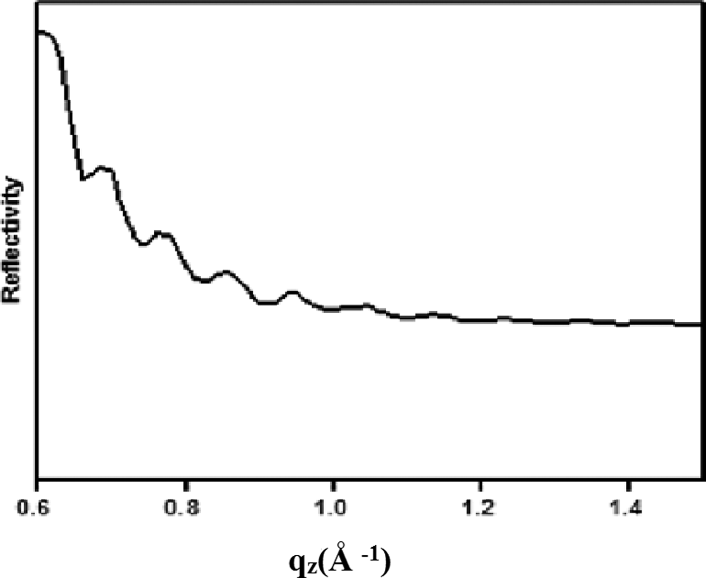
X-ray reflectivity is an extremely effective, accurate, and nondestructive technique for measuring the thickness, density, and microscopic surface roughness (Banerjee et al., 2006). Longitudinal specular and off-specular data were collected for grazing incidence X-ray reflectometry using the X-ray wavelength of 1.54 A0. Recursive formalism has been used for data analysis (Avila et al., Reference Avila, Montero, Galan, Ripalda and Levy2001). Figure 3 shows X-ray reflectivity data of typical C-SiC films depicting the surface roughness and thickness of film to be 0.4 nm and 94 nm and that of SiC film to be 119 nm and 1.2 nm, respectively. Films were found to be very smooth. Thickness values of some typical films were compared with the values obtained by different methods, i.e., specular reflection (not shown here) and from the cross-section FESEM image of other typical films (vide infra) and the results were matching.
X-ray reflectivity spectra of a typical SiC film.
FTIR Studies
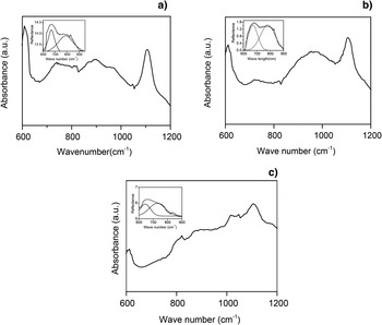
It is known that both cubic and hexagonal polytypes of SiC possess an infrared (IR) active mode around 800 cm−1. Position of this peak depends on crystallinity and surroundings of SiC precipitates. Detailed IR absorption studies of the SiC films deposited as such and in annealed form and the data are shown in Figures 4a and 4b. As deposited film shows a band centered around 667 cm−1, 780 cm−1, and at 1055 cm−1 (Fig. 4a) whereas a typical 2 h vacuum annealed SiC film shows bands centered around at 669 cm−1, 794 cm−1 along with other minor dips at 1055 cm−1(Fig. 4b). The absorption band in between 667 cm−1 and 800 cm−1 becomes more flat with increasing the annealing temperature and there is a red shift of 790 cm−1 band toward 794 cm−1, thus improving the Si-C bond formation with an improvement of the distribution of bond angle and bond length. The shape of the band centered around 794 cm−1 evolves in Gaussian form to a Lorentzian form that reflects a distribution of Si-C bond lengths and angles in an amorphous phase, whereas the Lorentzian shape reflects minimal bond angle distortion and bond length dispersion characterizing the crystalline phase (Kerdiles et al., Reference Kerdiles, Berthelot and Gourbilleau2000). Tabbal et al. (Reference Tabbal, Said, Hannoun and Christidis2007) reported the IR absorption data due to Si-C deposited at two laser energy level, i.e., at 200 and 400 mJ and found the peaks due to SiC occur as low as 765 cm−1 with a red shift toward 800 cm−1 and above as the laser energy increases to 400 mJ. The results obtained here corroborates with the reported result (Kusumori et al., Reference Kusumori, Muto and Brito2004). The peaks were found to be broad in nature due to the presence of both crystalline and amorphous SiC phases along with minor carbon phases (vide Raman spectra). Presence of a minor peak centered at 1055 cm−1 assigned to Si-O stretching vibration is attributed to interstitial oxygen impurities dissolved in Si substrates (Avila et al., Reference Avila, Montero, Galan, Ripalda and Levy2001).
FT-IR spectra of: (a) As deposited SiC film (b) annealed SiC film at 800°C for 2 hr (c) carbon film deposited on SiC film.

Micro-Raman Analysis
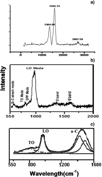
Raman scattering is more sensitive to atomic bonding of the materials and provides structural information about the powders and films. Figure 5 show micro-Raman spectra of as deposited SiC (Fig. 5a), annealed SiC (Fig. 5b), and C-SiC thin films (Fig. 5c). In order to gather the detailed information of Raman scattering, deconvolution was carried out for the broad bands in the spectra and respective peak positions were determined by fitting the spectra with a Lorentzian line shape. The results are displayed in the respective figures wherever needed.
Raman spectra of (a) As deposited SiC film (b) annealed SiC film at 800°C for 2 hr (c) C-SiC film.

As deposited film (Fig. 5a) shows weak bands at 776 cm−1, 810 cm−1, 966 cm−1 due to TO and LO optical mode of SiC (more clearly shown in annealed film in Fig. 5b) along with a broad peak at 1460 cm−1 due to the presence of amorphous C-C clusters of varying intensity. This 1460 cm−1 band on deconvolution result D and G Raman bands centered at 1430 cm−1 and 1550 cm−1, respectively.
It is known that with increase in the dielectric constant of the surrounding medium results in the downshift of the band positions from the TO and LO phonons of the particles. The dielectric constant of this C-C phase is about 3.5–5 and less than that of air (ɛair = 1). Hence, there was also a downshift of these modes here and the peak at 776 cm−1 and 966 cm−1 may have originated from the vibrational mode due to 4H-SiC, whereas the peak at 810 cm−1 may be due to the surface phonon modes and appear as result of Frohlich transitions enhanced by SPP. This mode dominates when the crystallite size is less than λ/π (=160 nm) where λ is 514.5 nm. Here the grain size lie in the range of 10–20 nm (FESEM result ) but the crystallite sizes were found to lie in between 2.3 to 3 nm (vide infra). Raman spectra collected at 30 s exposure with depth analysis showed similar pattern that confirms homogeneous distribution of amorphous carbon/graphene along with a combination of amorphous and crystalline SiC (vide infra).
But further carbon ion depositions onto the C rich SiC thin film, the 1430 cm−1 band gets blue shifted to 1364.06 cm−1 whereas 1550 cm−1 band gets red shifted to 1593.74 cm−1 and there appear D and G band at 1364.06 cm−1 and at 1593.74 cm−1 due to disordered graphitic phases along with second order two-dimensional (2D) at 2687.59 cm−1 (Figs. 5b and 5c). The presence of a strong G band along with 2D band reveals the presence of multilayer graphene formation. D peak at 1364.06 cm−1 signals the presence of defects and domain boundaries. Perrone et al. (Reference Perron, Maccioni, Chiolerio, Martinez De Marigorta, Naretto, Pandolfi, Martino, Ricciardi, Chiodoni, Celasco, Scaltrito and Ferrero2009) reported similar Raman spectra types of C-SiC, prepared by thermal decomposition of 4H-SiC. Red shift of graphitic band toward 1594 cm−1 could be due to the presence of number of C-C chains that are the basic units for formation of carbon nano-tube. Hence, here presence of carbon nano-tube at the interface can not be ruled out. Depending on the different techniques used, D and G band for different carbon can exist from 1200 cm−1 to about 1600 cm−1 (Veres et al., Reference Veres, Toth and Koos2008).
The Raman bands due to pure graphite, polycrystalline graphite, glassy amorphous carbon, diamond like carbon, graphene, diamond, carbon nanotube (filled and unfilled form) have been thoroughly discussed by Ferrari et al. (Reference Ferrari, Meyer, Scardaci, Cassiraghi, Lazzeri, Piscanec, Jhiang, Novoselov, Roth and Gelm2006) and also by Behera et al. (Reference Behera and Roul2008) with importance of the shape and intensity of the D, G, 2D, and G' bands. Detailed about the density functional theory regarding this has been also discussed in their articles.
The Raman spectra of EG grown on C-SiC and Si terminated SiC (Si-SiC) differ. It can be inferred from Figure 5 that it contains defects demonstrated by a stronger induced “D” band. The G band due to C-SiC and Si-SiC have the same frequency around 1594 cm−1 and are affected by the SiC substrate due to similar stress (Mattaush et al., Reference Mattausch and Pankratov2007). As observed only in case of C-SiC, both D and 2D bands are at lower band frequency i.e., at 1593.74 cm−1 and 2687.59 cm−1, respectively, in comparison to respective Raman bands that of graphene on Si-SiC. Very recent studies show that the immediate carbon layer to SiC does not contribute to the electronic behavior but the free carbon layer above that is responsible for the same. Hence, carbon films on SiC were observed under TEM at different places of the films and micro-structures along with EDAX analysis of the typical graphene films have been obtained (vide infra).
The graphitic crystallite size was determined from I(D) and I(G) bands using the following equations given by Tuinstra and Koeng et al. (Reference Tuinstra and Koenig1970)
 $$\hbox{I\lpar D\rpar /I\lpar G\rpar } = \hbox{C}\lpar {\rm \lambda} \rpar /\hbox{L}_{\rm a}\comma \;$$
where I (D) and I(G) are the intensity of the D and G bands and λ is the wavelength of the laser, i.e., 514.5 nm and C(λ) is found to be 4.4 nm. La is the crystallite size. Using these value of C(λ), I(D) and I(G) values obtained in case of typical C-SiC, La was found to be 2.33 nm. On analyzing other films crystallites size varying from 2.3 to 3.0 nm were obtained.
Films were found to be smooth with roughness values in the range 0.3 nm to 1.5 nm. Dense films with particle size below 20 nm were observed whereas the crystallite size was found to be 2.3–3 nm (C/SiC), which probably is the cause of the existence of the surface phonon mode at 810–840 cm−1 (vide Raman and FTIR results). It is interesting to note that SPP band occur at 810–840 cm−1 range in all the SiC thin films and this is probably due to the dominance of the scattering by the short range interaction at SiC/graphene interface (Dawlaty et al., 2011) and also is responsible for the anomalous dielectric behavior at this junction. As reported by Qazi et al. (Reference Qazi, Nomani, Chandrashekhar, Shields, Spencer and Koley2010) polariton enhanced reflectivity at SiC/graphene interface plays an important role to overcome the diffraction limit of light, especially applicable to nano-photonic devices. Here the light is converted to polariton at this interface that exhibits much shorter wavelength than a traveling EM wave giving a much smaller footprint on chip. An interesting phenomena is that these optical signal can be processed as a polariton and whenever needed, can be converted back to light transmission that means it can be used as efficient plasmonic waveguides. Hence, C-SiC film made here finds application in nano-photonics devices.
Presence of a sharp Raman peak at 520 cm−1 attributes to the LO mode of micro-crystalline Si is not shown in the Figures. On annealing drastic decrease of the intensity of Si peak at 520 cm−1 occur depicting the formation of Si-C bond. These micro-crystalline Si dissolute in amorphous carbon thus making stoichiometric/non-stoichiometric SiC films depending on the extent of Si dissolution in carbon (Jung et al., Reference Jung, Park, Mendieta and Smith2003), thus, enhancing the hardness of the films. The depth analysis studies show similar types of Raman spectra that depicts about homogenous distribution of very small C crystallites in the SiC matrix making the film hard.
FESEM Studies
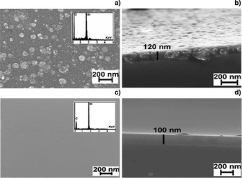
Surface morphological studies were carried out for all these films using field emission scanning electron microscope at 8 kV and WD value at 3.1 mm. Figures 6a and 6b show the micrographs of the deposited film with a smooth texture with its cross sectional image showing film thickness of 100 nm. Figures 6c and 6d show that of the typical C- SiC film showing the film thickness to be 120 nm. Inset in Figures 6a and 6c show the respective elemental analysis of Silicon and Carbon in SiC film as well as C-SiC film. According to the EDX analysis of SiC and C-SiC films the weight percentage of Si and carbon were found to be 27.76:68.20 and 39.2:.61.8, respectively. The SiC films were found to be smooth with 0.3 nm surface roughness whereas in case of C-SiC films this value increased to 1.5 nm. Also, the films were found to be dense and hard as observed under FESEM. This is probably the surface mobility of the high energy ablated species at the substrate surface, which gets enhanced because of the low mean free path of these particles as compared to target to substrate distance (4 cm here).
FESEM images of (a) As deposited SiC film with inset showing the elemental Si and carbon distribution (b) cross-sectional view of as deposited SiC film showing thickness of the film (c) C-SiC film with inset showing the elemental Si and carbon distribution (d) cross-sectional view of C-SiC film showing thickness of the film.

Transmission Electron Microscope Tests
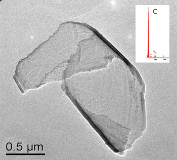
Figure 7 shows the micro-structures of the epitaxial graphene of typical film. It clearly shows transparent layered graphene structures. EDAX analysis also reveals the presence of only carbon. But broader Raman 2D band for typical films show multilayer. Hence, it can be inferred that although the films are thick in nature but they occur in free standing mode. Mattaush et al. (Reference Mattausch and Pankratov2007) emphasized that the carbon layer adjacent to the substrate does not contribute to the electronic structure. The free standing graphene layer exhibiting weak van der Waal's bonding to the underlying layer. Hence, attempts were made to study these free standing graphene layers.
Transmission electron micrograph showing transparent graphene layers.

Nano-indentation Tests
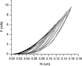
Figure 8 shows typical load viz. height curves of SiC films. Similar types of pattern are also obtained for C-SiC films. As discussed earlier in the experimental stage, hardness and elastic modulus values were determined for SiC, C-SiC films obtained by nano-indentation technique and were found to be 18 GPa, 37 GPa with elastic modulus values 290 GPa and 473 GPa, respectively. The films were dense as observed under FESEM with distribution of nano-grains of C, graphene, SiC nano-crystallites making the film very hard up to 37 GPa.
Load viz. height curve of the SiC film obtained from Nano-indentation test.

All these properties of SiC and graphene rich SiC films (C-SiC) studied here can give insight in understanding the materials used in making terahertz oscillators, nuclear fusion wall materials, and fast communications materials and also understanding the phenomena of polariton enhanced reflectivity at the SiC/graphene interface, making better Schottkey diodes etc.
CONCLUSIONS
Detailed FTIR, micro-Raman, FESEM, X-Ray reflectivity, TEM and Nano-indentation data analysis of the pulse laser deposited SiC and C-SiC thin films have confirmed formation of hard C, SiC crystallites (both in amorphous and crystalline form) along with graphene formation on the 4H-SiC surfaces. This material shows the presence of surface phonon polariton in the range of 810–840 cm−1 formed at SiC/graphene interface that finds application in nano-photonics related plasmonic wave-guide research and also in understanding the laser irradiation effects on SiC based nuclear fusion wall material.
ACKNOWLEDGMENTS
The authors thank the Director, CSIR-Institute of minerals and materials technology, Bhubaneswar for giving permission to publish the paper. One of the authors Bijayalaxmi Sahoo gratefully acknowledges the Council of Scientific and Industrial Research for the research fellowship. We thank Ms. Swagatika and Mr. Ajit for their technical support for getting FTIR, Raman spectra. This work carried out under CSIR-INDIAs nanostructured programme at advanced materials technology department, Bhubaneswar, Odisha, India.