Introduction
Terahertz (THz) technologies have been widely used in the applications such as remote sensing, radar, short-range communications in recent years [Reference Siegel1, Reference Song and Nagatsuma2]. For the applications of THz receivers/transmitters integrated with on-chip antennas (OCAs), it is strongly desirable to design efficient and compact antennas. Assisted by the advances in silicon technologies such as (Bi)CMOS, the system-on-chip approach has triggered significant interest, as it allows on-chip integration of digital baseband and complete RF front ends, alleviating the need of transitions from one technology to another [Reference Cheema and Shamim3]. OCAs have been designed based on several types such as quasi-Yagi [Reference Hsu, Wei, Hsu and Ru-Chuang4], slot [Reference Behdad, Shi, Hong, Sarabandi and Flynn5], dipole [Reference Neculoiu, Muller, Tang, Laskin and Voinigescu6], patch [Reference Seok, Shim, Mao, Han, Sankaran, Cao, Knap and Kenneth7], and inverted-F [Reference Zhang, Sun and Guo8] in silicon technology. However, it is challengeable to design a high-gain OCA. Most of the power is confined in the silicon substrate instead of radiating into free space due to the high dielectric constant and low resistivity of the substrate. In [Reference Hsu, Wei, Hsu and Ru-Chuang4], a 60-GHz on-chip Yagi antenna fabricated with 0.18-μm CMOS process achieves a measured gain of −10 dBi. In [Reference Behdad, Shi, Hong, Sarabandi and Flynn5], an X-band on-chip slot antenna is designed using 130-nm CMOS process. The antenna gain is −4.4 dBi. In [Reference Neculoiu, Muller, Tang, Laskin and Voinigescu6], an on-chip dipole antenna operating in the 160-GHz frequency range is presented. The antenna is fabricated in the 130-nm SiGe HBT with BiCMOS9 backend technologies. The antenna gain is −10 dBi. In [Reference Seok, Shim, Mao, Han, Sankaran, Cao, Knap and Kenneth7], an on-chip patch antenna fabricated in 45-nm CMOS process is demonstrated. The antenna gain is about −7 dBi. In [Reference Zhang, Sun and Guo8], a 60-GHz on-chip inverted-F antenna fabricated in CMOS technologies shows a gain of −19 dBi at 61 GHz.
In this paper, a 260 GHz on-chip cavity-backed dual-slot antenna is presented. The antenna is fabricated with 0.13-μm SiGe BiCMOS process. Our previous design reported in [Reference Li, Xiao, Feng, Li, Zhu and Yao9] is similar to the proposed antenna in this paper. The simulated model used in [Reference Li, Xiao, Feng, Li, Zhu and Yao9] was a little different from the final fabrication antenna proposed in [Reference Li, Xiao, Feng, Li, Zhu and Yao9]. Some modification to the simulated model in [Reference Li, Xiao, Feng, Li, Zhu and Yao9] has been made which ensures accordance with the final fabricated antenna. The modified antenna, proposed in this paper, has been fabricated and measured. The differences between two designs will be given in ‘Antenna design’ section. The slot antenna is backed with a thin cavity formed by several inner metal layers and vias in between. The cavity improves the impedance matching and radiation performance of the slot antenna. By adopting dual-slot and cross-shaped feed line, the bandwidth of the dual-slot antenna with cross-shaped feed line is significantly enhanced by 196% compared with the single-slot antenna with straight feed line. The antenna shows a measured impedance bandwidth of 15.2 GHz from 248.2 to 263.4 GHz. The simulated and measured gains of the cavity-backed dual-slot antenna are −1.3 and −2.1 dBi, respectively.
Antenna design
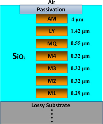
Figure 1 illustrates the lateral view of the chip environment used in this paper. The total thickness from the top metal layer (AM) to the bottom metal layer (M1) is around 17.12 µm. The Si substrate has a thickness of 250 µm. Above AM layer, there is a passivation layer with a thickness of 4.3 µm.
Lateral view of the chip environment.

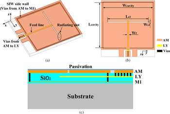
Initially, a cavity-backed single-slot antenna is designed as shown in Fig. 2. The single radiation slot is implemented on the top metal layer (AM). For exciting the operating frequency at around 260 GHz, the length of the slot can be roughly determined by:
 $$f = \displaystyle{c \over {2l\sqrt {\varepsilon _{re}}}}, $$
where c is the light speed in the air, and l is the length of the slot. A SIW cavity is formed by the top metal layer (AM) connected to the bottom metal layer (M1) through vias in between. The single-slot antenna is fed by a stripline placed on the LY metal layer. The feeding stripline is connected to the bond pad through vias from the AM layer to the LY layer. The M1 layer is used as a ground plane.
The geometry of the cavity-backed single-slot antenna (not to scale). (a) Three-dimensional view of the antenna. (b) Top view of the antenna. (c) Cross-section view of the antenna.

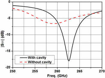
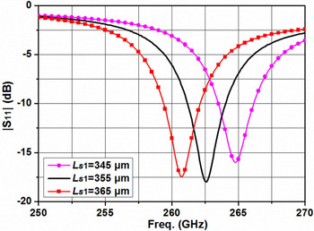
The SIW cavity is designed to improve the impedance matching and the radiation performance of the single-slot antenna. The simulated reflection coefficient results of the single-slot antennas with cavity and without cavity are presented in Fig. 3. It can be seen that the −10 dB impedance bandwidth of the cavity-backed single-slot antenna is 2.8 GHz from 261.2 to 264 GHz. The impedance matching of the single-slot antenna without cavity is poor. The length of the slot L s1 is a key parameter to tune the resonant frequency of the single-slot antenna. Simulated reflection coefficients of the single-slot antennas with different L s1 are plotted in Fig. 4. The frequency band almost remains unchanged in width, but shifts down to lower frequency band as L s1 increases, which proves that the position of the resonant frequency of the single-slot antenna is determined by the slot length L s1.
Simulated reflection coefficients of the single-slot antennas with and without SIW cavity.

Reflection coefficients of dual-slot antennas with different L s1.

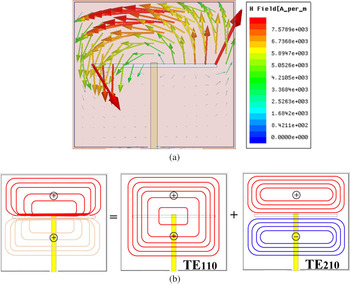
Field distributions in the SIW cavity of the single-slot antenna have been plotted in Fig. 5. It can be seen that a hybrid mode is excited in the SIW cavity at 262.5 GHz. The similar analysis of PCB SIW cavity hybrid mode has been presented in [Reference Luo, Hu, Li, Zhang, Sun and Zheng10]. From Fig. 5(a), it can be found that its H-field vector distribution is divided into an upper half cavity part and a lower half cavity part by the radiating slot. The fields distributing in these two parts are in phase. The dominant field is distributing in the upper half cavity part. Figure 5(b) shows that the hybrid mode at 262.5 GHz is a combination of a strong TE 110 resonance and a weak TE 210 resonance.
(a) H-field vector distribution at 262.5 GHz in the cavity of the single-slot antenna. (b) Dominant E-field isoline of a hybrid mode at 262.5 GHz.

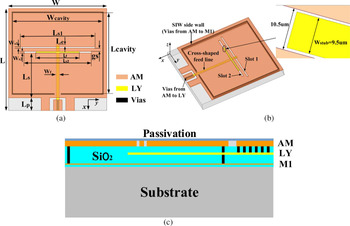
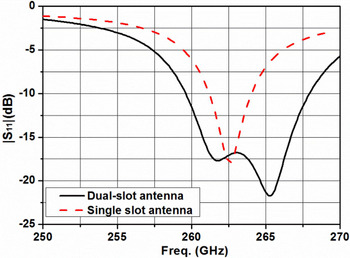
To improve the bandwidth of the cavity-backed single-slot antenna, another shorter radiating slot is added and a cross-shaped feed line is adopted, as shown in Fig. 6. An open stub along y-axis is added to form the cross-shaped feed line. All the other dimensions of the dual-slot antenna have the same values compared with the cavity-backed single-slot antenna. The simulated reflection coefficient result of the cavity-backed dual-slot antenna with cross-shaped feed line is presented in Fig. 7. The simulated −10 dB impedance bandwidth of the cavity-backed dual-slot antenna is 8.3 GHz from 259.6 to 267.9 GHz which has been enhanced by 196% compared with the one of the cavity-backed single-slot antenna with straight feed line. It can be seen that another new resonant frequency is generated at 265.3 GHz. Then an enhanced impedance bandwidth can be achieved by merging these two resonating frequencies close to each other. The optimized parameters of the on-chip cavity-backed slot antenna are listed in Table 1.
The geometry of the cavity-backed dual-slot antenna (not to scale). (a) Top view of the antenna. (b) Three-dimensional view of the antenna. (c) Cross-section view of the antenna.

Simulated reflection coefficients of the cavity-backed dual-slot antenna with cross-shaped feed line and cavity-backed single-slot antenna with straight feedline.

Optimized parameters of the on-chip cavity-backed dual-slot antenna

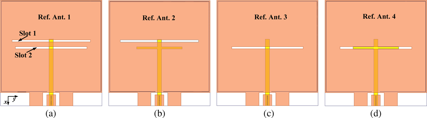
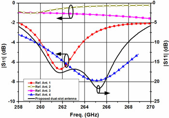
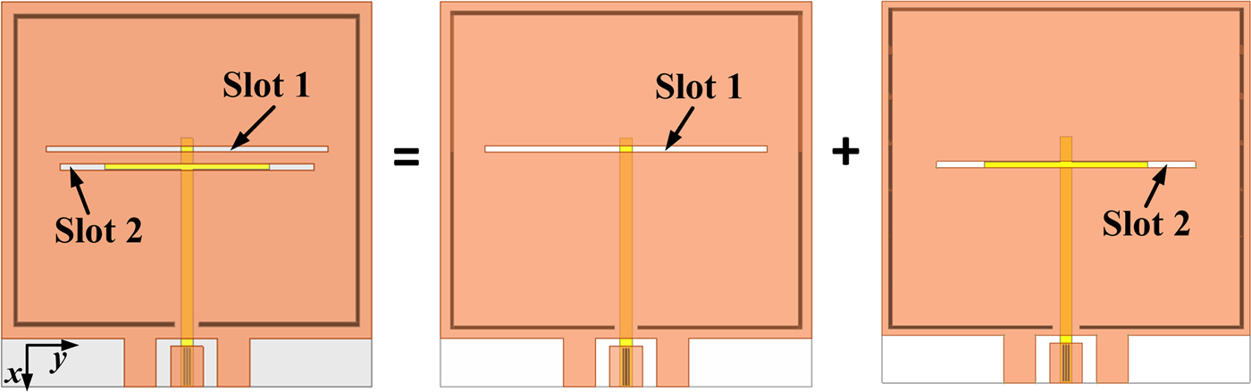
Four referenced antennas have been designed for comparison to better understand the bandwidth enhancement, as shown in Fig. 8. The simulated reflection coefficients of the four referenced antennas are presented in Fig. 9. From the simulated results of Ref. Ant.1 and Ref. Ant. 2, it can be found that adding an shorter radiating slot only or modifying the feed line only cannot generate a new resonant frequency to enhance the bandwidth of the antenna presented in Fig. 2. From the simulated result of Ref. Ant. 4, it can be concluded that the new resonant frequency at 265.3 GHz is excited by the added shorter slot 2 and the cross-shaped feed line as shown in Fig. 8(d). Based on the analysis above, the proposed cavity-backed dual-slot antenna can be equivalent to a combination of a cavity-backed single (long) slot with straight feed line and a cavity-backed single (short) slot with cross-shaped feed line, as shown in Fig. 10. The simulated H-field vector distributions in the cavity at 265 GHz of these three antennas are plotted in Fig. 11. The H-field vector distribution in the cavity at 265 GHz of the proposed cavity-backed dual-slot antenna can be regarded as a hybrid mode.
Four referenced antennas. (a) Cavity-backed dual-slot antenna with straight feed line. (b) Cavity-backed single (long) slot antenna with cross-shaped feed line. (c) Cavity-backed single (short) slot antenna with straight feed line. (d) Cavity-backed single (short) slot antenna with cross-shaped feed line.

Simulated reflection coefficients of four referenced antennas and the proposed cavity-backed dual-slot antenna.

Hybrid equivalent model of the proposed cavity-backed dual-slot antenna.

H-field vector distributions at 265 GHz of the hybrid equivalent model.

It is noted that the simulated model in this paper is a modified one based on [Reference Li, Xiao, Feng, Li, Zhu and Yao9] we have reported. In [Reference Li, Xiao, Feng, Li, Zhu and Yao9], the cavity in the simulated model was formed by via holes with the same size (2 µm × 2 µm) between every two adjacent metal layers, which simplified and accelerated the simulation process because this simplified model significantly reduced the amount of the via holes in the simulation. However, this simplified design was different from the actual fabrication process, which resulted in big deviation between simulated and measured results as shown in [Reference Li, Xiao, Feng, Li, Zhu and Yao9]. Some modifications have been made to the via holes model in the current proposed design according to the design rules. The simulated models of via holes in this paper and in [Reference Li, Xiao, Feng, Li, Zhu and Yao9] are shown in Fig. 12. The sizes of different types of via holes used in this paper are presented in Table 2. Some main parameter values of the proposed antenna in this paper have been modified accordingly as shown in Table 3.
Two kinds of via hole-simulated models (not to scale). (a) Used in Ref. [Reference Li, Xiao, Feng, Li, Zhu and Yao9]. (b) Used in this paper.

Dimensions of different types via holes used in this paper

Comparison of optimized parameter values in [Reference Li, Xiao, Feng, Li, Zhu and Yao9] and in this paper (unit: μm)

Results and discussions
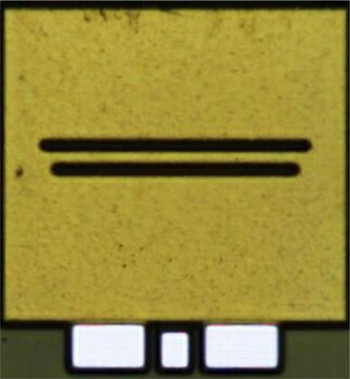
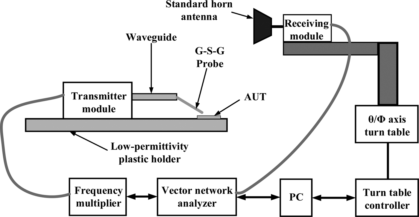
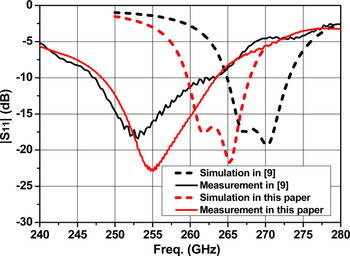
The proposed antenna was fabricated using 0.13-μm SiGe BiCMOS technology. Figure 13 shows the micrograph of the fabricated cavity-backed dual-slot antenna. The antenna was measured with the setup shown in Fig. 14. A ground–signal–ground probe with a pitch of 100 µm is touched on the grounded coplanar waveguide line of the proposed antenna for measurement. Figure 15 shows that the measured and simulated −10 dB impedance bandwidths are 15.2 GHz from 248.2 to 263.4 GHz and 8.3 GHz from 259.6 to 267.9 GHz, respectively. It can be seen that compared with [Reference Li, Xiao, Feng, Li, Zhu and Yao9], the simulated reflection coefficient agrees even better with the measured one after the modification to the via holes simulated model. Considering such a high operating frequency, a 3% deviation of about 8 GHz between simulated center frequency and measured center frequency is acceptable. The discrepancy between the simulated results and measured results mainly results from measurement setup and the deviation of the substrates characteristics settings in the simulation from their actual values.
Micrograph of the fabricated cavity-backed dual-slot antenna.

Schematic diagram of the measurement setup.

Simulated and measured reflection coefficients of the antennas in this paper and Ref. [Reference Li, Xiao, Feng, Li, Zhu and Yao9].

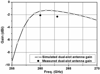
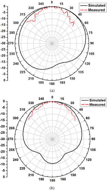
Simulated and measured gains of the proposed dual-slot antenna are presented in Fig. 16. The simulated peak gain of the dual-slot antenna is −1.3 dBi. The measured gains at 260 and 263 GHz are −2.1 and −2.3 dBi, respectively. The simulated maximum radiation efficiency is 31.1%. Simulated and measured radiation patterns at 260 GHz of the proposed dual-slot antenna are shown in Fig. 17. Due to the presence of certain obstacles in the probe station, only the radiation patterns within ±50° are obtained. The ripples of the radiation patterns are probably due to the interference between the probe and the antenna during measurement.
Simulated and measured gain of the proposed cavity-backed dual-slot antenna.

Simulated and measured radiation patterns of the proposed cavity-backed dual-slot antenna at 260 GHz. (a) E (xoz)-plane. (b) H (yoz)-plane.

Conclusion
This paper presents a study of the performance of an on-chip cavity-backed dual-slot antenna fabricated with 0.13-μm SiGe BiCMOS process. The SIW cavity is designed to improve the impedance matching and the radiation performance of the antenna. Bandwidth enhancement is achieved by adopting dual-slot structure and cross-shaped feed line. The proposed on-chip cavity-backed dual-slot antenna shows the advantages of high gain and compact size. It demonstrates that the proposed antenna can be a promising candidate for THz communication systems.
Acknowledgements
This work is supported in part by the project 6140518040116DZ02001 from the Equipment Development Department of the Central Military Commission, in part by the project 61601050 from the National Natural Science Foundation of China (NSFC). The authors would like to thank GLOBALFOUNDRIES for the fabrication support.
 Jun Xiao received the B.Eng. degree and the M.Eng. degree from Harbin Institute of Technology, Harbin, China, in 2008 and 2011, respectively. He is currently working toward the Ph.D. degree in electronic science and technology at the Beijing University of Posts and Telecommunications, Beijing, China. His research interests include millimeter-wave antennas and THz antennas.
 Zihang Qi received the B.Eng. degree in 2013. He is currently pursuing the Ph.D. degree with the Beijing University of Posts and Telecommunications, Beijing, China. His current research interests include millimeter-wave/THz antennas and microwave filters.
 Xiuping Li received the B.S. degree from Shandong University in 1996, the Ph.D. degree from Beijing Institute of Technology in 2001. From 2001 to 2003, she joined in Positioning and Wireless Technology Center, Nanyang Technological University in Singapore, where she was a research fellow and involved in the research and development of RFID system. In 2003, she was a research professor in Yonsei University, Seoul, South Korea. Since 2004, she joined Beijing University of Posts and Telecommunications, Beijing, China, as an associate professor and was promoted to professor in 2009. She is currently the vice dean of School of Electronic Engineering, Beijing University of Posts and Telecommunications, Beijing, China. She has been selected into the New Century Excellent Talents Support Plan in National Ministry of Education, Beijing Science & Technology Nova Support Plan, in 2007 and 2008, respectively. She won the second prize of progress in science and technology, Chinese Institute of Communications in 2015. She was the recipient of the awards of Distinguished Youth Teacher of Beijing in 2017, Excellent Teacher of Beijing in 2017. She is the author of four books, over 100 journal and conference papers. She was also awarded more than 20 PRC patents. Her current research interests include millimeter-wave antennas, THz antennas, RFID systems, and MMIC design.
 Weiwei Feng received the B.Eng. degree in 2012. He is currently pursuing the Ph.D. degree with the Beijing University of Posts and Telecommunications, Beijing, China. His current research interests include millimeter-wave/THz circuits.
 Hua Zhu received the M.S. degree from Guilin University of Electronic Technology, Guilin, China, in 2010, and the Ph.D. degree from Beijing University of Posts and Telecommunications, Beijing, China, in 2015. She is currently a lecturer of Beijing University of Posts and Telecommunications, Beijing, China. Her research interests include UHF RFID beam scanning antenna array design in complex environment and millimeter-wave/terahertz antenna design.