


Introduction
Diamonds, with a wide bandgap of ∼5.4 eV, are electrical insulators and exhibit tremendous inertness to radiation as well as to chemical corrosion.Reference Himpsel, Knapp, van Vechten and Eastman1 Diamonds are known for the various properties these materials possess, such as extreme mechanical hardness, high bulk modulus (low compressibility) (1.2 × 10¹² N/m2), high thermal conductivity (2 × 10³ Wm–1 K–1), and low thermal expansion coefficient at room temperature (0.8 × 10⁻⁶ K–1 ) (see the Introductory article in this issue).Reference Walker2 Among these, the potential application to cold cathodes and field emission cathodes are of special interest. The versatility of the chemical vapor deposition (CVD) technique has enabled the development of diamond films with tailor-made properties.Reference Goodwin, Butler, Prelas, Popovici and Bigelow3,Reference Celii and Butler4 Ultrananocrystalline diamond (UNCD) films are a special category of diamond film with a grain size less than ∼10 nm,Reference Krauss, Auciello, Gruen, Jayatissa, Sumant, Tucek, Mancini, Moldovan, Erdemir, Ersoy, Gardos, Busmann, Meyer and Ding5,Reference Williams, Daenen, D’Haen, Haenen, Maes, Moshchalkov, Nesládek and Gruen6 which is versatile for microstructural control and modification of physical properties.Reference Jiao, Sumant, Kirk, Gruen, Krauss and Auciello7,Reference Correa, Wu, Wen, Chandrasekharan and Shannon8
This article is aimed at illustrating the different methods that have been adopted to change the granular structure, the doping composition, and the surface properties of diamond films, thereby enhancing the electronic properties of diamond films for the development of various kinds of electrons sources, especially cold electron emission from negative electron affinity (NEA) diamond and field emission/thermionic emission of electrons from UNCD films.
Cold electron emission from NEA diamond films
The NEA nature of hydrogen-terminated diamond surfaces has been given attention for the realization of robust and high-efficiency cold cathodes even though intrinsic diamond films are insulating in nature. There are two possible approaches to utilize the benefit of the NEA of the hydrogen-terminated diamond surface: (1) through the fabrication of diamond p–n junction and (2) the secondary electron emission from NEA diamond.
Diamond p–n junction NEA cathode
From recent studies based on total photoelectron yield spectroscopy, p-type and intrinsic diamond surfaces show good electron emission characteristics when they are terminated by hydrogen.Reference Takeuchi, Ogura, Ri, Kato, Okushi and Yamasaki9 However, these diamond films do not have conducting electrons to supply for electron emission from their surfaces. In the case of n-type diamond, which also shows NEA when its surface is hydrogen terminated, electrons are thermally excited to the conduction band from which they are expected to easily escape into vacuum. Still, a low electron emission yield was observed.Reference Takeuchi, Ogura, Ri, Kato, Okushi and Yamasaki9 In subsequent studies, this was attributed to charge transfer at the surface, which leads to upward band bending, thereby suppressing electron emission.Reference Yamada, Hasegawa, Kudo, Masuzawa, Okano and Nebel10 A convincing result of successful diamond p–n junction fabrication was reported in 2001, for the first time forming boron-doped and phosphorus-doped CVD diamond layers epitaxially on {111} single crystalline diamond substrates. The junctions showed clear diode characteristics and ultraviolet light emission at 235 nm, which proves minority carrier injection for both sides of p- and n-type diamond layers through the junction interface (i.e., electron injection from the n-type to the p-type layer [electrons are the minority carrier for p-type semiconductors] and hole injection from the p-type to the n-type layer [holes are the minority carrier for n-type semiconductors] through the p-n junction interface are taking place concurrently).Reference Koizumi, Watanabe, Hasegawa and Kanda11 This was a new opportunity to fabricate efficient electron emitters using electron injection into p-type diamond.
Hydrogen-terminated diamond surfaces naturally show NEA in vacuum with very high thermal and chemical stability due to the strong covalent bonding of C–H. The surface is stable even after exposure to air or heating to over 400°C. Based on this, exploratory research was performed with the aim of obtaining p–n junction cold cathodes fabricated from diamond. Initially, the electron efficiencies of these devices were lower than 0.01% due to poor junction fabrication. Most problems related to junction fabrication are due to the difficulties in obtaining n-type diamond.Reference Geis, Efremow, Woodhouse, McAleese, Marchywka, Socker and Hochedez12,Reference Brandes, Beetz, Feger and Wright13
After establishing n-type diamond growth, followed by the successful formation of p–n junctions, a study of efficient p–n junction cold cathodes was first reported in Japan in 2006.Reference Koizumi, Ono and Sakai14 Diamond p–n junctions were formed on {111} single crystalline diamond surfaces because high-quality n-type diamond was only feasible in this orientation. A phosphorus doped n-type diamond layer was deposited as a bottom layer for the p–n junction on the {111}-oriented diamond substrate. Growth was performed by microwave plasma CVD. Phosphine (PH3) was used as a dopant gas together with methane and hydrogen as source gases. The film thickness was 5 µm, with a phosphorus doping concentration of 1 × 1019 cm−3. On the surface of the n-type diamond, using diborane as the doping source gas, a boron-doped p-type diamond layer was formed with a thickness and doping concentration of 500 nm and 1 × 1018 cm−3, respectively. After the p–n stacking, mesa structures were fabricated by reactive ion etching in order to obtain p–n junction diodes.Reference Koizumi, Ono and Sakai14
Electron emission measurements were performed in an ultrahigh vacuum (UHV) probe station. The sample was placed on the stage of the UHV probe station, which was heated to 200°C to obtain higher conductivity of the n-type layer, which has a large donor activation energy of 0.57 eV. A collector electrode, biased at 100 V, was placed above one of the p–n junction mesas with about 0.1 mm separation. The p–n junction showed rectifying diode characteristics, and electron emission from the p-type layer of the p–n junction was observed in the forward bias regime by which the diode turns on. The electron emission efficiency (electron emission current/diode current) of the first prepared device was 0.64%.Reference Koizumi, Ono and Sakai14
By improving the crystalline quality of the semiconducting diamond layers, the emission efficiency was increased up to 1.4%, as reported in 2009.Reference Koizumi and Kono15Figure 1 shows the current-voltage characteristics of the latter diamond p–n junction cathode together with the electron emission efficiency plots. It is clear that the electron emission strongly increases with forward diode current increase. In the reverse bias regime, clear leakage in the diode current is observed, although no increase in the electron emission current appears. In subsequent work, electron emission current densities of ∼0.23 A/cm2 have been obtained with excellent emission current stability.Reference Takeuchi, Koizumi, Makino, Kato, Ogura, Ohashi, Okushi and Yamasaki16 These results confirmed that the electron emission is driven by electron injection at the p–n junction interface. The emission area and energy of emitted electrons have been carefully analyzed using electron emission spectro-microscopy.Reference Kono and Koizumi17 The electron emission image clearly showed the emission coming from the p-type diamond surfaces on top of the mesa structures. The energy of the emitted electrons was about 4 eV over the Fermi level of p-type diamond (∼0.37 eV from the valence band maximum) with an energy spread of about 1 eV. It was considered that electrons, injected from the n-type layer, drift in the conduction band of p-type diamond and occupy empty surface states of the hydrogen-terminated surface. A part of those electrons escape to the vacuum when their energy is higher than the vacuum level. The emission current, formed by these electrons, can be measured with a collector electrode.
Electron emission and diode characteristics of a diamond p–n junction cathode.Reference Koizumi and Kono15

The application of p–n junction cold cathodes as high voltage switching devices has been successfully demonstrated.Reference Takeuchi, Koizumi, Makino, Kato, Ogura, Ohashi, Okushi and Yamasaki16Figure 2 shows the concept drawing of a high voltage vacuum switch using a diamond p-i-n junction cold cathode. In the near future, it is expected to obtain efficient ultrahigh voltage switches, which can serve as DC high voltage transmission systems for electricity, preferably used in offshore wind power generation.
A schematic drawing of the proposed vacuum switch and the electrical characterization circuit is shown. E represents the high voltage of the power supply, IA the anode current (or the current of the high voltage line), Z the load, VA the anode voltage, VL the voltage drop at the load, VG the control voltage of the electron emitter, and IG the control current of the electron emitter. IA = IG + IK, and in the on state, VA = Von, which is the on-voltage of this switch. In the off state, VA = E.Reference Takeuchi, Koizumi, Makino, Kato, Ogura, Ohashi, Okushi and Yamasaki16
Secondary electron emission from NEA diamond
While efficient electron emission at NEA diamond surfaces has been confirmed experimentally,Reference Himpsel, Knapp, van Vechten and Eastman1,Reference Bandis and Pate18–Reference Diederich, Aebi, Kuttel and Schlapbach20 electrons must be present in the conduction band in order to exploit this NEA emission capability. One practical approach is to inject electrons into the conduction band using energetic electron or photon beams.Reference Jenkins and Trodden21 In such a process, the impacting beam loses energy through electron scattering, whereby valence electrons are excited into the conduction band. These “secondary” electrons can then diffuse through the conduction band to the NEA surface, where they can be emitted into a vacuum (Figure 3a).
(a) Schematic energy-band representation of the secondary-electron-emission process in diamond produced by an impacting electron beam with energy E0. (b) Energy distribution curves measured from the hydrogenated surface of 8-μm-thick single crystal diamond flake in reflection and transmission configurations.Reference Yater, Shaw, Jensen, Feygelson, Myers, Pate and Butler22 (c) Secondary emission gain measured from NEA surfaces (cesiated, Cs; hydrogenated, H) of single-crystal natural diamond (C(100), C(111)) and polycrystalline (CVD) diamond films.Reference Yater and Shih25
A key feature of such an emission from NEA diamond is the narrow energy spread of the emitted electrons (FWHM < 0.5 eV).Reference Himpsel, Knapp, van Vechten and Eastman1,Reference Yater, Shaw, Jensen, Feygelson, Myers, Pate and Butler22 This results from thermalization during the transport process as the secondary electrons (with an incident energy E0) lose energy through phonon scattering. Consequently, the electron distribution that reaches the surface is dominated by very-low-energy electrons. At surfaces with positive electron affinity, this distribution is blocked by the energy barrier, and only the relatively few non-thermalized electrons can be emitted. However, at the NEA surface, the entire secondary electron distribution can be emitted, resulting in electron beams with low energy spread (Figure 3b).
Additionally, large current amplification can be achieved when energetic electron beams impact a NEA diamond film. Specifically, incident electrons with energy E0 generate a cascade of secondary electrons, with the internal gain being approximately equal to E0/(2.5 × Eg) (where Eg is the bandgap energy).Reference Klein23,Reference Jensen, Yater, Shaw, Myers, Pate, Butler and Feygelson24 Consequently, a single impacting electron can produce ∼73 secondary electrons for each keV incident energy, thereby providing a current multiplication mechanism in the diamond. Importantly, if a sufficiently large percentage of secondary electrons reach the surface, emission currents can be obtained that are substantially higher than the incident current. In fact, emission gains as high as ∼115 and ∼85 were measured at E0 = 2.9 keV from hydrogenated p-type single-crystal and polycrystalline diamond films, respectivelyReference Yater and Shih25,Reference Shih, Yater, Pehrsson, Butler, Hor and Abrams26 (Figure 3c).
In spite of such results, high emission gain cannot be achieved at all hydrogenated diamond surfaces. Rather, the emission gain depends on the dynamics of the generation, transport, and emission processes.Reference Jenkins and Trodden21 Specifically, the internal gain increases with E0, but the penetration depth of the primary beam increases as well. Thus, to optimize the transport efficiency of secondary electrons, high crystal quality is important to limit scattering and traps at defects and grain boundaries, while sufficient conductivity and downward band bending are needed to promote electron transport to the surface.
To optimize the emission probability, a uniform NEA must be present across the surface that is stable and robust in a practical operating environment. In general, the hydrogenated diamond surface meets these criteria, as it is stable in vacuum up to ∼800°C, and the NEA property can be restored after exposure to air by moderate annealing (∼400°C) to remove surface adsorbates.Reference Thoms, Pehrsson and Butler27 In fact, the hydrogenated diamond surface is exceptionally robust and stable when compared to surface coatings (e.g., CsO, BaO) used in state-of-the-art thermionic and photocathode materials. However, in situ annealing of the diamond may not be possible in practical device applications, and the hydrogenated surface may also degrade following sustained high-energy particle impact (e.g., electrons, photons, ions).Reference Shih, Yater, Pehrsson, Butler, Hor and Abrams26,Reference Mearini, Krainsky, Wang, Dayton, Ramesham and Rose28,Reference Hopman, Verhoeven, Bachmann, Wilson and Kroon29 Strategies are needed to overcome these challenges, and research efforts are exploring possible approaches. For example, a robust, air-stable NEA surface has recently been demonstrated on lithium-covered oxygen-terminated diamond that exhibits the same high emission efficiency as the hydrogenated surface.Reference O’Donnell, Edmonds, Ristein, Tadich, Thomsen, Wu, Pakes and Ley30
Additionally, a transmission approach has been demonstrated that uses back-side electron beam impact to avoid damage at the NEA emitting surface.Reference Yater, Shaw, Jensen, Feygelson, Myers, Pate and Butler22,Reference Chang, Wu, Ben-Zvi, Burrill, Kewisch, Rao, Smedley, Wang, Muller, Busby and Dimitrov31 Due to the longer transport through the film, a fully thermalized electron distribution reaches the surface with very low energy spread (∼0.3 eV) (Figure 3b).Reference Yater, Shaw, Jensen, Feygelson, Myers, Pate and Butler22 However, efficient transport becomes especially critical in order to achieve high emission gain. Therefore, it is necessary to use very thin films (e.g., microns thick) of high-purity single-crystal diamond, along with an internal field to accelerate the electrons to the surface. While challenging, the successful development of a high-gain transmission-mode secondary emitter would permit the current amplification of existing electron sources and thereby provide previously unattainable emission performance.
Exciting opportunities exist to exploit the current amplification capabilities of NEA diamond, as well as the low energy spread of the emitted electrons, in a wide range of device applications, including cathodes for vacuum electronics, electron beam lithography, electron multiplier technology, and high-resolution imaging and spectroscopy.
Electron field emission from UNCD films
High conductivity UNCD films
UNCD films possess a very interesting granular structure that can be easily altered. In fact, most of the approaches for improving the conductivity of UNCD films via “doping” end up with modification of the granular structure of the films. One typical example is the enhancement of the electron field emission (EFE) properties of UNCD films via the ion implantation process. It has been demonstrated that P-, O-, N-, and Cu-ion implantationReference Hu, Ye, Liu, Shen, Chen and Hu32–Reference Panda, Sundaravel, Panigrahi, Magudapathy, Krishna, Nair, Chen and Lin36 as well as Au-ion irradiationReference Chen, Chen, Wang, Lee, Lin, Guo and Chang37–Reference Sankaran, Chen, Sundaravel, Lee, Tai and Lin39 improved the EFE properties of UNCD films. The conductivity of the UNCD films increased with dose for Au-ion implantation, achieving a value as high as σ = 185 S/cm when 1 × 10¹⁷ ions cm2 of Au-ions were implanted into the UCND films; the enhanced EFE properties were preserved even after annealing.Reference Chen, Teng, Tang, Sundaravel, Amirthapandian and Lin38,Reference Sankaran, Chen, Sundaravel, Lee, Tai and Lin39 The EFE process of such films can be turned on at 4.88 V/μm with an EFE current density of Je = 6.52 mA/cm2 at an applied field of 8.0 V/μm. TEM examination revealed that the Au ions formed clusters in the UNCD films that induced the formation of a nanographite phase surrounding the clusters.
Gruen et al.Reference Arenal, Bruno, Miller, Bleuel, Lal and Gruen40,Reference Lin, Sankaran, Chen, Lee, Chen, Lin and Tai41 demonstrated that using CH4/N2 plasma instead of CH4/Ar plasma yields needle-like diamond grains. It was also observed that UNCD films grown at 700°C (designated as N-UNCD) showed very good conductivity (σ = 200 S/cm) and superb EFE properties of E0 = 6.13 V/μm and an EFE current density of Je = 3.36 mA/cm2 at 8.8 V/μm.Reference Sankaran, Kurian, Chen, Dong, Lee, Tai and Lin42 TEM examination revealed that they contain needle-like diamond grains encased in a few layers of graphite. On the other hand, diamond films with a hybrid granular structure were developed using a unique two-step microwave plasma-enhanced (MPE)-CVD process in which a layer of UNCD film was first grown in CH4/Ar plasma to serve as a nucleation layer for subsequent deposition of a nano-diamond film using CH4/(50%Ar-50%H2) plasma.Reference Cheng, Chiang, Horng, Chen, Wang and Lin43,Reference Wang, Chen, Cheng and Lin44 The second MPE-CVD process resulted in the formation of large diamond aggregates evenly distributed in the matrix of ultra-small grains (i.e., a hybrid granular-structured diamond [HiD]). The HiD films showed even better EFE properties than the UNCD films (i.e., lower turn-on field of (E0)HiD = 6.6 V/μm and a higher EFE current density of (Je)HiD = 1.0 mA/cm2 at 30 V/μm applied field).Reference Cheng, Chiang, Horng, Chen, Wang and Lin43 N-ion implantation/annealing of the HiD films further improved the EFE properties of these films.Reference Panda, Chen, Sundaravel, Panigrahi and Lin45
These observations demonstrated that UNCD films are versatile in terms of modification of their granular structure. All of the ion-implantation, N2-plasma MPE-CVD, and two-step MPE-CVD processes thus can modify the granular structure of the UNCD films, rendering them more conductive. The key to enhancing the conductivity of the films is the induction of a nanographitic phase encasing the diamond grains.
Diamond nanostructures as electron field emitters
To further enhance the EFE behavior, two approaches have been adopted to fabricate electron field emitters with a high aspect ratio: (1) the use of nanoscale tips as templates for growing high conductivity UNCD films and (2) directly fabricating diamond nanowires (DNWs) via a reactive ion etching (RIE) process. Si-nanowires (SiNWs) are good candidates for this application. The UNCD films can be grown on SiNWs with full coverage, exhibiting good EFE properties (i.e., with a low turn-on field of E0 = 4.4 V/μm and a large EFE capacity of J2 = 13.9 mA/cm2 at an applied field of Ea = 12.0 V/μm).Reference Tzeng, Lee, Lee, Lin and Chiu46,Reference Tzeng, Liu, Lee, Lin, Lin, Lee and Chiu47 The alternative is to fabricate Si-pyramids (Sipyramid, 4 μm in size and 3.5 μm in height with a pyramid separation of 10 μm) using an RIE processReference Chang, Lou, Chen, Chen, Lee, Tai and Lin48 that are less sharp but are widely separated. Superior EFE behavior was observed. The evident feature of the HiD/Si-pyramid emitters is that the template fabrication process is robust since standard photolithographic and RIE processes are the only techniques required for making these nanostructures.
In some applications, such as microplasma devices, the cathode materials are subjected to continuous ion bombardment. To fabricate electron field emitters, which combine good EFE properties with high resistance to Ar-ion bombardment in a microplasma, high conductivity N-UNCD films were directly reactive ion etched using Au nanodots as masking materials,Reference Sankaran, Kunuku, Lou, Kurian, Chen, Lee, Tai, Leou, Chen and Lin49 resulting in high conductivity diamond nanowires (N-DNWs) with σ = 275 S/cm (Figure 4a). The N-DNWs exhibit high EFE properties with a turn-on field of (E0)N-DNWs = 2.04 V/μm and a large EFE current density of (Je)N-DNWs = 4.84 mA/cm2 at an applied field of Ea = 3.2 V/μm (Figure 4b). These N-DNWs emitters also show good stability against the plasma bombardment when used as a cathode material in a microplasma device (inset, Figure 4c).
Scanning electron microscope micrograph of ultrananocrystalline diamond (UNCD) nanorods after (a) and before (b) the reactive ion etching process; (c) the electron field emission properties of reactive ion etched UNCD nanorods, with the TEM microstructure and a selected area electron diffraction image of the UNCD films shown as an inset. (d) The lifetime test for a microplasma device, in which the UNCD nanorod was used as a cathode (the inset shows the typical plasma illumination images of the device).Reference Sankaran, Kunuku, Lou, Kurian, Chen, Lee, Tai, Leou, Chen and Lin49
The other approach of developing the electron emitter is to utilize the advantage of sp 2- and sp 3-bonded carbons that was demonstrated in the NCD-coated carbon nanotubes (CNTs).Reference Sankaran, Srinivasu, Leou, Tai and Lin50 Coating a thin layer of NCD film on CNTs markedly improved the stability of CNT emitters, although it slightly degraded the EFE properties. Such a composite material utilized both the advantage of the high conductivity/large aspect ratio of CNTs and the negative electron affinity/high hardness of the diamond film, resulting in emitters that possess very good EFE properties with high stability against plasma bombardment. The NCD-coated CNTs possess a low turn-on field (E0) of 2.19 V/μm and an emission current density (Je) of 2.33 mA/cm2 at an applied field of 4.76 V/μm. There was no noticeable current degradation or fluctuation over a period of 250 min at an applied voltage of 900 V, whereas the bare CNT emitters lasted only 33 min at an applied voltage of 360 V.Reference Sankaran, Srinivasu, Leou, Tai and Lin50
Flexible electronics possess great potential for applications and are of large current interest. The high EFE emitters described previously are all based on Si substrates and are very rigid. For the purpose of fabricating flexible EFE emitters, a transfer process was adopted in one study, as shown schematically in Figure 5a.Reference Sankaran, Tai and Lin51 The flexible EFE emitters are comprised of pyramidal N-UNCD tips on a polynorbornene-based polymer, shown in the photograph in Figure 5a. This EFE emitter exhibited good EFE properties; it can be turned on at (E0)flexible = 2.2 V/μm, achieving a high EFE current density of (Je)flexible = 5.10 mA/cm2 at an applied field of Ea = 6.0 V/μm (Figure 5b). These EFE emitters show high brightness on a flexible phosphor screen, which was separated from the emitters by a flexible PTFE spacer (∼1 mm) (inset, Figure 5b). Moreover, the EFE current density can last more than 144 min without showing any sign of degradation. Such EFE behavior is superior to those of flexible electron field emitters previously reported (Table I).Reference Sankaran, Tai and Lin51–Reference Verma, Das, Lahiri and Choi55
(a) The process for fabrication of flexible diamond electron field emitters: (i) chemical etching of Si to form inverted cavities, (ii) growth of ultrananocrystalline diamond (UNCD) films on the Si containing the inverted cavities, (iii) coating of a thin Au layer, (iv) coating of a 10-mm-thick polynorbornene-based polymer (PNB) film, (v) etching of the Si materials, resulting in the UNCD pyramids on PNB, and (vi) a micrograph showing the flexible diamond electron field emitters. (b) The electron field emission properties of the flexible diamond electron field emitters, using 2, 4, 6, and 8 μm UNCD pyramids as emitting materials. The inset in (b) shows the typical field emission image for the devices using phosphor-coated polymer as the anode.Reference Sankaran, Tai and Lin51
Comparison of electron field emission properties of flexible C-UNCD pyramidal microtips with various flexible field-emitting materials.
a E0: the turn-on field defined as the applied field corresponding to the Je-value indicated in the parenthesis.
b Je: the EFE current density corresponding to the applied field specified.
c β: the field enhancement factor estimated from Fowler-Nordheim model (equation 2).
d τ: the life-time stability measurement under the current density indicated in the parenthesis.
Thermionic electron emitters
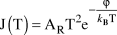
Conventional thermionic electron sources utilized in telecommunications, space propulsion, and energy conversion operate at temperatures in excess of 1000°C requiring extensive power management and systems design. For the direct transformation of heat into electricity a reduction in operation temperature would allow a more widespread deployment. Thermionic electron emission can be described by the Richardson-Dushman formalism (1) where the electron emission current density J(T) is given by:
 $${\rm{J}}\left( {\rm{T}} \right) = {\rm{A}}_{\rm{R}} {\rm{T}}^2 {\rm{e}}^{ - {{\phi } \over {k_B {\rm{T}}}}} {\rm{}}$$
where
 $${\rm{A}}_{\rm{R}} = {{4{\rm{\pi }}m_e k_B^2 e} \over h}^2 $$
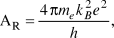
using Boltzmann’s constant, k B, electron mass, m e, electronic charge, e, work function, φ, and Planck’s constant, h, resulting in a theoretical value for the Richardson constant (AR) of 120 A/cm2 K2.
An emitter device can be realized by deposition of a thin doped diamond film on top of a nitrogen incorporated UNCD [(N)UNCD] layer where defect states can propagate through the structure. The observed low work function of these films suggested an origin in the mid-bandgap states due to structural defects in the nanometer-size grain boundaries.Reference Uppireddi, Westover, Fisher, Weiner and Morell56 The low work function observed for diamond emitters can, in part, be attributed to the hydrogen termination as it provides the negative electron affinity surface characteristics that eliminate a surface barrier for electron emission. The use of NEA diamond in a thermionic electron source necessitates examination of its temperature stability. Paxton et al. Reference Paxton, Howell, Kang and Davidson57 characterized a nitrogen-incorporated diamond film (work function of ∼2.2 eV) prepared on a molybdenum substrate, where hydrogen desorption was observed at around 700–800°C. The hydrogen coverage was related to the emission current density and value of the Richardson constant while no significant effect on the work function was observed.
Suitable metallic substrate materials for thermionic electron emission include refractory metals such as tungsten and molybdenum as they form low resistivity carbides during high-temperature diamond deposition and establish a stable interface for the emitter. A typical thermionic emitter comprised of a metallic substrate, a (N)UNCD interfacial layer, and a nitrogen-doped diamond top layer was characterized by a low work function <1.4 eV, where electron emission commenced at temperatures <250°C.Reference Koeck and Nemanich58 Diamond thin-film emitters deposited on various substrate materials exhibited a low work function, and the thermionic emission was described in terms of the Richardson-Dushman formalism, as shown in Figure 6a. The rhenium substrate-based emitter displayed a low work function of 1.34 eV; a significant Richardson constant of 53.1 A/cm2 K2; and sustained an emission current density of ∼44 mA/cm2 at a temperature of 530°C. The results indicated that interface carbide formation could limit emission presumably because of increased resistance, while a non-carbide-forming substrate with an increased Richardson constant effectuated significant emission enhancement.Reference Koeck and Nemanich59
(a) Thermionic electron emission from nitrogen-doped diamond structures prepared on various substrate materials.Reference Koeck and Nemanich59 (b) Schematic of a thermionic energy converter comprised of a thermionic emitter and collector separated by a vacuum gap, and (c) output power of a thermionic converter at various temperatures in vacuum and with atomic hydrogen in the inter-electrode gap resulting in significant and stable power output at an elevated temperature.Reference Koeck, Nemanich and Sharp77
Various doping levels available in diamond suggest their application in thermionic emitters with diminished work function. Suzuki et al.Reference Suzuki, Ono, Sakuma and Sakai60 measured a nitrogen-incorporated nanocrystalline diamond film prepared on silicon, and a work function of 1.99 eV was extracted from a fit to the Richardson equation. The higher work function in this report was attributed to strong upward band bending (∼1.6 eV).Reference Diedrich, Kuttel, Aebi and Schlapbach61 However, this value was obtained from a study on single crystal diamond surfaces. Kataoka et al. investigated thermionic electron emission from nitrogen-doped diamond films prepared on high-pressure high-temperature (HPHT) Type-Ib diamond plates with (001)-oriented surfaces, wherein the thermionic emission spectra yielded a photoelectric work function of 2.4 eV.Reference Kataoka, Zhu, Koeck and Nemanich62 This film sustained an emission current density of about 1.2 mA/cm2 at 740°C. For boron-doped nanocrystalline diamond films with hydrogen termination, a work function of 3.95 eV was reported.Reference Robinson, Show, Swain, Reifenberger and Fisher63 Measurements of sulfur-doped nanocrystalline diamond yielded a work function of 2.5 eV and a value for the Richardson constant of about 40 A/cm2 K2.Reference Koeck and Nemanich64 With phosphorus as the shallow donor, one of the lowest thermionic work functions of 0.9 eV was reported for films prepared on molybdenum substrates.Reference Koeck, Nemanich, Lazea and Haenen65 Enhancement of the thermionic electron current can be realized by ionization of gaseous species at low work function diamond surfaces.Reference Wurz, Schletti and Aellig66,Reference Scheer, Wieser, Wurz, Bochsler, Hertzberg, Fuselier, Koeck, Nemanich and Schleberger67 The Saha-Langmuir formalism describes this process.Reference Dresser68 In the ionization process, an electron is transferred to an unoccupied molecular orbital, establishing a negative ion state with lifetime τ.
Ionization of a gaseous particle occurs when it approaches the diamond surface where the vacuum level of the particle and the diamond surface vacuum level become aligned. If energetically suitable states are present in the diamond, an electron will tunnel to the affinity level of the particle establishing a negative ion. This phenomenon was employed in particle detectors utilizing diamond-like carbon surfaces.Reference Scheer, Wieser, Wurz, Bochsler, Hertzberg, Fuselier, Koeck, Nemanich and Schleberger69 Direct conversion of heat into electricity can be achieved by a process termed thermionic energy conversion, where a temperature gradient is established across a vacuum gap separating a thermionic electron emitter from a collector electrode.Reference Hatsopoulos and Gyftopoulos70 The efficiency of such a device can exceed 30% but cannot surpass 90% of the Carnot cycle efficiency.Reference Houston71 Initial thermionic energy conversion measurements from a nitrogen-doped diamond emitter demonstrated a self-generated thermo-voltage of 0.23 V at ∼750°C.Reference Koeck, Garguilo and Nemanich72 In a similar measurement, a low work function (N)UNCD-based emitter was separated from a similar collector by a 50 μm vacuum gap. At an emitter temperature of 500°C, an electrical potential difference of about 0.5 V was measured across the gap, and the power dissipated in a variable ohmic load indicated direct conversion of heat into electricity.Reference Koeck, Nemanich, Balasubramaniam, Haenen and Sharp73 A different approach utilized field emission at elevated temperatures from nitrogen-doped CVD diamond with a work function of ∼1.2 eV. Enhanced emission of thermally excited electrons was suggested for power generation at high temperatures.Reference Shin, Fisher, Walker, Strauss, Kang and Davidson74,Reference Fisher75 Paxton et al. observed a low work function of 1.39 eV from nitrogen-incorporated “ridged” nanodiamond films synthesized on highly doped n-type silicon where an emission current of ∼0.5 µA at 900°C was measured, suggesting its application for thermal energy conversion.Reference Paxton, Wisitsoraat, Raina, Davidson and Kang76
The power output of a thermionic energy converter (Figure 6b) can be enhanced by increasing the charge released from the emitter (i.e., adding to the thermionic current an ionic component generated by surface ionization phenomena at the emitter). Performance enhancement can, in part, be attributed to a reduction in space charge effects. Results from a UNCD-based thermionic energy converter in vacuum and methane (electron affinity level of 0.083 eV) ambient indicated generation of a negative ion current across the gap, resulting in increased power output with a concurrent shift of maximum power output to lower load resistance.Reference Koeck, Garguilo and Nemanich72,Reference Koeck, Nemanich, Balasubramaniam, Haenen and Sharp73 Nitrogen-doped diamond films with a work function of ∼2 eV enabled charge transfer to atomic hydrogen (electron affinity level of 0.75 eV). It should be noted that the resonant tunneling process benefits from a widening of the affinity level as the atomic species approaches the surface. The increase in the device current and thus output power was attributed to the charge the negative hydrogen ions transferred across the gap (see Figure 6c).Reference Koeck, Nemanich and Sharp77
Summary
Electron sources are found in a variety of devices ranging from traveling wave tubes for telecommunications, cathodes for free electron lasers, thrusters for space propulsion, and direct heat to electricity power converters. New interest in high data rate communications in the THz regime presents an opportunity for diamond electron sources. Similarly, efficient electrical energy generation could be feasible through diamond-based thermionic electron emitters. The status of the development of various kinds of electron sources, including cold electron emission from NEA diamond and field emission/thermionic emission of electrons from UNCD films, has been reviewed. In p–n junction NEA cathodes, electrons are injected from n-type diamond to the conduction band of p-type diamond, giving rise to electron emission with efficiencies exceeding 1%. Alternatively, impacting electron beams are used to produce secondary electron emission from NEA diamond, with emission gains of more than 100 being demonstrated. By exploiting the NEA surface properties, exciting opportunities exist to further advance the development of novel diamond cold cathode technology for a wide range of commercial applications, including high voltage switching devices, high-power amplifiers, linear accelerators, and x-ray sources.
Concerning the electron field emission of UNCD films, the N-UNCD and HiD films show the best EFE properties. In both films, the formation of a nanographitic phase is presumed to be the prime factor that enhanced the EFE properties of the materials. Two approaches have been demonstrated to be effective in enhancing the EFE behavior of the electron field emitters: (1) utilization of nano-tips as templates for growing high conductivity UNCD films and (2) direct fabrication of diamond nanostructures via the RIE process. Thermionic electron sources based on diamond utilize NEA surface characteristics and the ability of the lattice to accept impurities to engineer a low work function emitter. Utilizing rhenium as a non-carbide-forming substrate and highly conducting nitrogen-incorporated UNCD films in the emitter structure realized an efficient thermionic electron source that established an emission current of ∼44 mA/cm2 at a temperature of 530°C. Thermionic energy conversion in such a diluted gaseous ambient significantly enhances power output.
Acknowledgment
R.J.N. acknowledges the support of the Office of Naval Research under grant N00014–10–1-0540. K.H. acknowledges the support of the Research Foundation Flanders (FWO) under grants G.0555.10N and G.0456.12.



