I. INTRODUCTION
Studies of transition metal dichalcogenides (TMDs) and the search for monolayers or two-dimensional (2D) systems are not new; monolayers of TMDs consist of metal layers sandwiched by sulfur, selenium, or tellurium atomic layers. Wilson and Yoffe Reference Wilson and Yoffe1 published a seminal paper in which the physicochemical properties of TMDs are described in detail. Perhaps the first work on MoS2 exfoliation by the adhesive type method resulting in few-layer MoS2 and monolayers of MoS2 is the work of Frindt. Reference Frindt2 One year earlier, the same author published a manuscript in which the optical properties of few-layered MoS2 were reported Reference Frindt3 : In this manuscript, the differences between the absorption spectra of thin (few layers) and bulk MoS2 were established. Later, Joensen et al. Reference Joensen, Frindt and Morrison4 published an article entitled “single-layer MoS2” obtained by lithium intercalation. Here, it was found that after drying the exfoliated MoS2, the material restacked in a random fashion. As in graphite and hexagonal boron nitride, layered systems of TMDs (including inorganic fullerenes and nanotubes) are held together by weak van der Waals forces that make them suitable for lubrication. Reference Fleischauer5–Reference Rapoport, Fleischer and Tenne7 It is noteworthy that these inorganic fullerenes and nanotubes of TMDs are formed by introducing curvature to the inorganic sheets. Reference Tenne, Margulis, Genut and Hodes8–Reference Tenne, Margulis and Hodes10
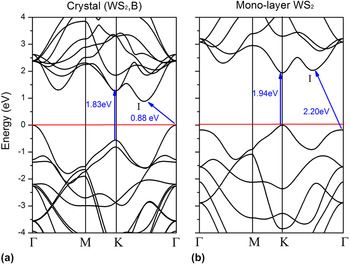
As stated in the abstract, TMDs could exhibit semiconducting (indirect and direct band gaps) and metallic behaviors depending upon their composition, structure, and number of layers. In addition, they could possess two main crystallographic phases: trigonal prismatic and octahedral (less stable). The trigonal prismatic crystal structure of MoS2, MoSe2, WS2, and WSe2 corresponds to indirect band gap materials, whereas their octahedral phases are metallic. Reference Mattheis11–Reference Petkov, Billinge, Heising and Kanatzidis15 In metallic systems such as NbS2 and NbSe2, even the same trigonal prismatic structure (the same as the semiconducting TMDs already mentioned above) reveals a metallic behavior, Reference Wilson and Yoffe1,Reference Rahn, Hellmann, Kallane, Sohrt, Kim, Kipp and Rossnagel16–Reference Seifert, Terrones, Terrones and Frauenheim18 and these metals could also exhibit charge-density wave instabilities. Reference Moncton, Axe and Disalvo19,Reference Malliakas and Kanatzidis20,Reference Rahn, Hellmann, Kallane, Sohrt, Kim, Kipp and Rossnagel16 What makes the trigonal prismatic semiconducting TMDs very special is that as the number of layers decrease, the material becomes a direct band gap semiconductor when reaching a monolayer, Reference Mak, Lee, Hone, Shan and Heinz21 thus making it suitable for optical applications Reference Zeng, Dai, Yao, Xiao and Cui22–Reference Chhowalla, Shin, Eda, Li, Loh and Zhang30 (see Fig. 1).
Band structures for WS2 showing the direct band gap K–K and the indirect band gap Г–I for (a) WS2 crystal (b) WS2 monolayer. The line at 0 eV shows the top of the valence band.

Regarding early calculations of single layers of TMDs, Bromley et al. Reference Bromley, Yoffe and Murray31 used a semi empirical tight binding method for generating the band structures of MoS2, MoSe2, WS2, WSe2, and α-MoTe2; however, the direct band gap features for the monolayers were not observed using this approach. Later, calculations using density functional theory (DFT) and GW approaches confirmed the direct band gap existence at the K point Reference Lebegue and Eriksson32–Reference Terrones, Lopez-Urias and Terrones37 (see Fig. 1). It looks like this direct band gap behavior is restricted only to monolayers of TMDs, but to the best of our knowledge, there are no studies so far demonstrating that bilayers might reveal a direct band gap. Therefore, a detailed study on the electronic behavior of bilayers becomes necessary including different stackings of monolayers with the same TMD composition, and heterolayers with different types of layered materials, and this is precisely the aim of this work.
Our calculations indicate that bilayer WS2 with different stackings reveals different band structures in which the energy differences between the direct and indirect gaps are small. Nevertheless, the indirect band gap continues to be dominant. This behavior can also be extended to the other semiconducting TMDs such as MoS2, MoSe2, and WSe2 (see below). To our surprise, when studying heterobilayer systems of TMDs (WS2–WSe2, MoS2–MoSe2, WSe2–MoS2, and MoSe2–WS2), direct band gaps, half in energy of those reported for monolayers, are found for some cases in which the diselenide layer is sandwiched with a disulfide layer. Reference Terrones, Lopez-Urias and Terrones37 These direct band gaps range from 0.79 to 1.16 eV. Therefore, the study of heterobilayers of TMDs becomes relevant for designing and constructing novel optoelectronic materials. At the same time, metallic and semiconducting bilayer heterostructures have been also calculated finding that all the systems studied possess a metallic behavior, but with unique features above the Fermi level for the MoS2–NbSe2 and WS2–NbSe2 systems that are discussed in the following sections.
A. Band gap competition in different stackings of TMDs
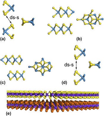
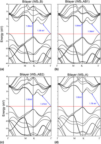
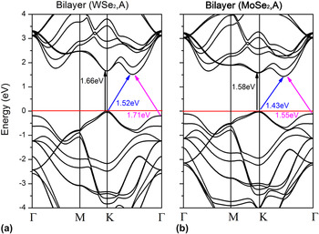
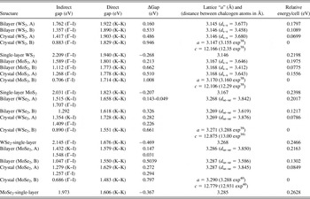
To shed light on the behavior of bilayers of TMDs with different stackings, four cases of WS2 bilayers have been studied: (i) crystal-type stacking called bilayer (WS2, B), where B stands for bulk. This is the stacking presented in the WS2 triangular prismatic phases of TMDs, where the metal atoms are on top of the sulfur atoms [see Fig. 2(a)]; (ii) bilayer (WS2, AB1) stacking in which the layers are displaced such that the transition metal atoms of one layer are in the center of the hexagonal WS2 rings of the other TMD layer as shown in Fig. 2(b); (iii) bilayer (WS2, AB2) where the displacement produces the metal atoms of one layer to be on top of metal atoms of the other, and the sulfurs on one layer in the center of the hexagonal WS2 rings of the other layer [see Fig. 2(c)], and (iv) bilayer (WS2, A) in which the metal atoms are on top of metal atoms and chalcogen atoms on top of chalcogen atoms [see Fig. 2(d)]. When calculating these systems using DFT-local density approximation (LDA) (see Sec. IV), it was found that the smallest gap difference between direct (K–K) and indirect (Г–I) band gaps for the bilayer (WS2, A) was 0.16 eV (see Fig. 3). However, in all cases the indirect band gap dominates with gap differences ranging from 0.53 eV in bilayer (WS2, B) to 0.16 in bilayer (WS2, A). In addition, both the direct and indirect band gaps change when modifying the stacking, and it was also noted that the indirect band gap exhibits a more significant change from 1.36 to 1.76 eV (see Fig. 3). Since the smallest difference of direct and indirect band gaps is achieved with stacking type A, we have calculated the direct and indirect band gaps for other semiconducting TMD bilayers considering stacking A for MoS2, WSe2, and MoSe2 (see Table I). Interestingly, it was found that bilayer (WSe2, A) reveals a smaller direct band gap at K–K when compared to the indirect band gap Г–I, with a difference of 0.049 eV, nevertheless, the material continues being an indirect band gap semiconductor since the indirect band gap K–I is smaller than the direct band gap at K [see Fig. 4(a)]. A similar behavior is presented by the bilayer (MoSe2, A), where the difference between direct band gap K–K and indirect band gap Г–I is very small with a value of 0.031 eV [see Fig. 4(b)]. Therefore, the diselenide bilayers show a different electronic behavior from the disulfides [see Fig. 2(e)]. In general, for bilayers and the crystals of MoS2, MoSe2, WS2, and WSe2, the stacking type A possesses a smaller band gap than the stacking type B found in the trigonal prismatic phases. However, stacking type B are more favorable in energy (see Table I).
Different stackings for bilayer WS2 systems obtained by displacing one layer with respect to the other. (a) Side and top view of bulk like stacking or bilayer(WS2, B); the arrow shows the distance between chalcogen “d s–s” atoms between the layers. (b) Side and top view of AB1-type stacking or bilayer(WS2, AB1). (c) Side and top view of AB2-type stacking or bilayer(WS2, AB2). (d) Side and top view of A-type stacking or bilayer(WS2, A); the arrow shows the distance between chalcogen “d s–s” atoms between the layers. (e) Heterobilayer of MoS2 and MoSe2.

Band structure for different WS2 bilayer stackings showing the directs K–K band gap and the indirect band gap Г–I. (a) bilayer(WS2, B), (b) bilayer(WS2, AB1), (c) bilayer(WS2, AB2), (d) bilayer(WS2, A). The line at 0 eV shows the top of the valence band.

(a) Band structure for the bilayer(WSe2, A) showing the direct K–K band gap (black) and the indirect Г–I (magenta) and K–I (blue) band gaps. Note that the direct band gap is smaller than the indirect Г–I for this case. (b) Band structure for the bilayer(MoSe2, A) showing the direct K–K band gap and the indirect Г–I and K–I band gaps. Note here that the direct band gap and the indirect band gap Г–I are very close. However in both cases (a) and (b), the indirect band gaps K–I are smaller than the direct band gap; this might be observed experimentally by photoluminescence or optical absorption techniques. The line at 0 eV shows the top of the valence band.

Semiconducting TMDs' properties as calculated with DFT-LDA showing the indirect band gap, the direct band gap, the difference between direct and indirect gaps, lattice parameters, distance between chalcogen atoms (d s–s or d se–se) between the two layers in parenthesis, and relative energies per cell. In the case of the crystals for which the experimental lattice parameters are known, these are put in parenthesis with the prefix “exp.”

B. Semiconducting heterobilayers of TMDs
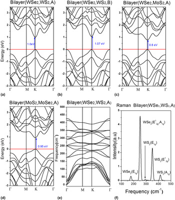
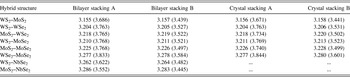
Motivated by the results discussed above, 24 heterobilayers of TMDs (MoS2, MoSe2, WS2, and WSe2) have been calculated using the DFT-LDA approach considering crystalline phases with different stackings. To name these systems, the following nomenclature was used: bilayer (MoS2, WSe2, A), where it is established if the system is a bilayer or a crystal, in parenthesis, the first two indices correspond to each of the TMDs involved, and the third index reveals the type of stacking as shown in Sec. I. A (B for bulk and A as shown in Fig. 2). These systems can be categorized into four groups depending on their band structure as shown in Table II. Reference Terrones, Lopez-Urias and Terrones37 Interestingly, some cases exhibit direct band gaps at the K point, which are approximately half of those found in the pure single layers (see Table II and Fig. 5). Details of these systems have been published recently. Reference Terrones, Lopez-Urias and Terrones37 Therefore, direct band gap semiconductors out of heterobilayers are possible if diselenides are mixed with disulfides. It is worth mentioning that to achieve this, the disulfide layer needs to be expanded and the diselenide exhibits a small reduction. The distance between chalcogen atoms between layers (see Fig. 2) is larger for the stacking type A than for the stacking type B (see Table III); therefore, the interlayer distance is slightly bigger in the stacking type A. Despite the strain, phonon dispersion calculations indicate that these systems are structurally stable showing no imaginary frequencies [see Fig. 5(e)]. In addition, the phonon dispersion provides the vibrational modes observed in Raman spectroscopy which are closer to the experimental values Reference Terrones, Lopez-Urias and Terrones37 [see Figs. 5(e) and 5(f)].
Direct band gaps at K point in hetero bilayer semiconducting TMD. (a) Bilayer(WSe2, WS2, A), (b) bilayer(WSe2, WS2, B), (c) bilayer(WSe2, MoS2, A), (d) bilayer(MoS2–MoSe2, A). (e) Phonon dispersion of bilayer(WSe2, WS2, A). (f) Calculated Raman intensities of bilayer(WSe2, WS2, A).

Direct and indirect (in parenthesis) band gaps in eV of hybrids of semiconducting TMDs. Systems with a dominant direct band gap at the K point in the Brillouin zone have an asterisk “*”. Cases with “+” show an indirect fundamental band gap Γ–K, and “&” corresponds to a dominant indirect gap K–I.

Lattice parameters “a” in Å, and distance d s–se (in parenthesis, in Å) between chalcogen atoms between the two layers of the TMDs.

II. METALLIC HETEROBILAYERS OF TMDs
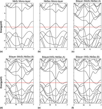
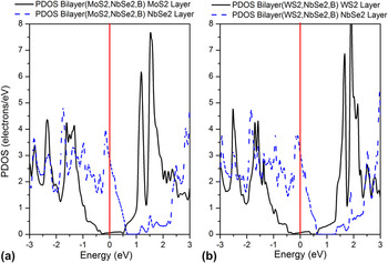
NbS2 and NbSe2 in bulk and their monolayers possess metallic behavior [see Figs. 6(a) and 6(b)]. Therefore, it is relevant to study heterobilayers of TMDs in which one layer is semiconducting and the other metallic. The studied cases include MoS2–NbS2, MoS2–NbSe2, WS2–NbS2, WS2–NbSe2, MoSe2–NbS2, MoSe2–NbSe2, WSe2–NbS2, and WSe2–NbSe2. It was found that all cases are metallic, however, the MoS2–NbSe2 and WS2–NbSe2 bilayer systems exhibit a particular band structure above the Fermi level for both stackings studied (A and B). Bilayer (MoS2–NbSe2, B) exhibited an interpenetration in the band structure, which increases for stacking A [see Figs. 6(c) and 6(d)]. For bilayer (WS2–NbSe2, B), there is a small band gap of 0.055 eV around 0.6 eV. This gap is reduced when the stacking becomes type A to 0.025 eV [see Figs. 6(e) and 6(f)]. As in the semiconducting heterobilayers, the interlayer spacing is slightly greater for stacking type A (see Table III). The partial density of states has also been computed to show that the electronic states at the Fermi level are due to the NbS2 layer, and the disulfide layer states play a role above the Fermi level around 0.6 eV, where a crossing or almost touching of bands occur (see Fig. 7); this suggest that doping or defects might shift the Fermi level to the band touching area, thus generating a new type of “semimetal” unique in TMDs.
Band structure of metallic TMD. (a) NbS2 monolayer, (b) NbSe2 monolayer, (c) bilayer(MoS2–NbSe2, A), (d) bilayer(MoS2–NbSe2, B), (e) bilayer(WS2–NbSe2, A), and (f) bilayer(WS2–NbSe2, B). The Fermi level is at zero.

PDOS of (a) bilayer(MoS2, NbSe2, B) and (b) bilayer(WS2, NbSe2, B). In both cases, the electronic states at the Fermi level are mainly due to the NbSe2 layer (Fermi level is at zero).

III. CONCLUSION
It has been shown first that different stackings of TMDs play a role in their electronic properties by changing the direct band gap at the K point and also the indirect band gap Г–I. Second, in the search for direct band gap materials with different stacking arrays exhibiting two layers of the same TMDs, it was found that although the direct and indirect band gaps become closer for a particular stacking (type A), the indirect band gap continues to dominate. However, when layers of disulfides and diselenides are sandwiched forming heterobilayer systems, a direct band gap is possible. This direct gap is half of that found in single layer TMDs, thus belonging to the infrared part of the spectrum, not to the visible as the monolayers of semiconducting TMDs. The application of these heterobilayer systems, which do not possess inversion symmetry, might find a place in new valleytronic devices. Third, heterobilayers of TMDs involving one metallic and one semiconducting layer have been analyzed finding that these exhibit metallic behavior with particular band features above the Fermi level, which might be exploited by doping or defects generating possibly new semi metallic bilayers of TMDs. Among the techniques used to synthesize these materials, chemical vapor deposition looks promising for obtaining different stackings and even different TMD layers. Reference Elías, Perea-López, Castro-Beltrán, Berkdemir, Lv, Feng, Long, Hayashi, Kim, Endo, Gutiérrez, Pradhan, Balicas, Mallouk, López-Urías, Terrones and Terrones41 Nevertheless, exfoliation techniques followed by annealing and pressure control might also prove useful for designing heterobilayer systems out of TMDs. Devices with heterolayers involving graphene (semimetal) and semiconducting TMDs such as WS2 have already proved to be useful as vertical field-effect transistors; Reference Georgiou, Jalil, Belle, Britnell, Gorbachev, Morozov, Kim, Gholinia, Haigh, Makarovsky, Eaves, Ponomarenko, Geim, Novoselov and Mishchenko42 therefore, the next step is to include different TMD heterostructures (semiconducting and metallic) with lattice that would match much better among them than with graphene or BN. The cases studied in this account open up the spectrum of possible applications for 2D materials (also termed van der Waals solids), thus adding new properties to the already known properties of graphene, hexagonal boron nitride, and single layer TMDs.
IV. METHODS
Our calculations have been performed using the plane wave code CASTEP, Reference Clark, Segall, Pickard, Hasnip, Probert, Refson and Payne43 on hexagonal cells under the LDA considering the Ceperley–Alder–Perdew and Zunger (CA–PZ) Reference Ceperley and Alder44,Reference Perdew and Zunger45 functional with 9 × 9 × 3 Monkhorst–Pack K-points and a plane waves cut off of 500 eV. All the structures were relaxed, including the cells, until the forces became smaller than 0.01 eV/Å and the energy tolerances were less than 5 × 10⁻⁶ eV/atom. A vacuum of 16 Å between the bilayers was considered. To select the optimum approach for interlayer distances, van der Waals interactions were considered through a dispersion correction (DFT-D) Reference Ortmann, Bechstedt and Schmidt46 under both the LDA and general gradient approximation (GGA-PW91). Reference Perdew, Chevary, Vosko, Jackson, Pederson, Singh and Fiolhais47 To test the results, several TMD structures were calculated such as WS2, MoS2, WSe2, MoSe2, NbSe2, and NbS2 and compared with the experimental data available. The lattice constant experimental values exhibit good agreement with the LDA approach (without considering the dispersion correction DFT-D). For the LDA-DFT-D, the layers get closer to each other producing a compactification of the “c” lattice parameter (around 3.6% smaller than bulk), whereas with the GGA-DFT-D approach, the layers get farther apart thus producing a lattice with a much larger “c” parameter (around 3.5% bigger than bulk). The lattice “c” parameters obtained with LDA produce the best fit within 1.5% or less of those reported experimentally. Moreover, our results are in agreement with those reported by other groups within the LDA formalism. Reference Ding, Wang, Ni, Shi, Shi and Tang48,Reference Mahatha, Patel and Menon49 Although GGA might usually provide corrections that best describe the system, for few-layer systems with van der Waals interactions such as TMDs, LDA provides better values (compared with the experimental) for direct optical band gaps and lattice parameters. Both the DFT and GGA underestimate the electronic band gap; however, due to a coincidence, the LDA direct band gaps agree better with the experimental optical transitions observed in the photoluminescence characterization of monolayer TMDs. Therefore, we decided to use LDA for all the calculations presented here. The phonon dispersion is calculated with the above parameters but extending the plane wave cut off to 720 eV using the density functional perturbation theory as implemented in the CASTEP code, which uses the linear response methodology that works well for insulators. Reference Refson, Tulip and Clark50
ACKNOWLEDGMENTS
This work is supported by the U.S. Army Research Office MURI Grant No. W911NF-11-1-0362, supported in part by the Materials Research Computing and Cyberinfrastructure unit of Information Technology Services and Penn-State Center for Nanoscale Science. M.T. also acknowledges support from the Penn State Center for Nanoscale Science for seed grant on 2-D layered materials (Grant No. DMR-0820404).