I. INTRODUCTION
Modern multi-band operation electronic devices require the development of efficient and compact multi-band filters. Indeed, the development of multi-band filters is a very active research field nowadays. Recently, many literatures addressing the design of multi-band bandpass filters (BPFs) are reported in [Reference Crnojević-Bengin1–Reference Lan, Weng, Ye and Hung17]. Advances in multi-band microstrip filters, edited by Vesna Crnojević-Bengin, were reported in [Reference Crnojević-Bengin1]. Dual-band filters using defected stepped impedance resonator (SIR), meandering SIR, modified SIR, and asymmetric stepped impedance stub-loaded multimode resonator have been investigated and reported in [Reference Wu, Liang, Qin and Lin2–Reference Pal, Ghatak and Sarkar5]. A stepped-impedance resonator connected with two short-circuited stubs was presented in [Reference Deng, Zhao, Zhang, Chen and Wang6]. In [Reference Tsai and Hsue7, Reference Chen, Hsu and Chuang8], dual-band bandpass filters were constructed using equal length coupled-serial-stunted lines and Z-transform techniques, dual-feeding structures, and embedded resonators. In [Reference Song, Zhang, Zhuge and Fan9–Reference Mondal and Mandal11], spiral resonators and short-circuited stub-loaded, stub-loaded multiple-mode resonator, and stub-loaded open-loop resonators have been used to construct dual-band bandpass filter. In [Reference Chen, Wu and Su12–Reference Lan, Weng, Ye and Hung17], multi-band BPFs, tri-, and quad-band, were also proposed. Therefore, to realize a multi-band BPF with compact size, high selectivity, and good performance simultaneously is still a challenge for circuit designers.
In this paper, a stub-loaded stepped impedance resonator is investigated and used to design a compact dual-band BPF centering at 2.4/3.5 GHz. First, the analysis odd-and even-mode equivalent circuits of the proposed stub-loaded stepped impedance resonator (SLSIR) are presented. Then, design equations are derived to guide the design of the circuits. Second, the configuration of the dual-band BPF with respect to the coupling schematic topology is presented. Analysis of the two passbands with respect to the cross-slots and open stub of the resonator are presented. Lastly, the circuits are constructed and simulated by the electromagnetic (EM) simulation software HFSS and IE3D, respectively. Measurement of the fabricated circuit is performed by a scalar network analyzer. Finally, the results are quantitatively compared with the other reported results in references.
II. DESIGN PROCEDURE
A. Analysis of the proposed resonator
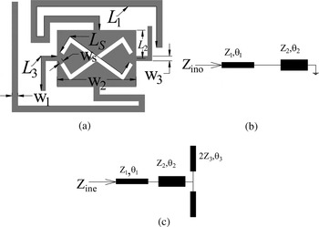
Figure 1 (a) is the proposed stub-loaded SIR. It is a stepped-impedance resonator with two open stubs and cross-slots. The SIR is characterized by its length 2(L 1 + L 2) and widths of (w 1, w 2). The two open stubs with uniform-impedance of width w 3 and length L 3 are connected to the middle of the low-impedance section line of SIR. Two cross-slots with width w S and length L S are placed in low-impedance section line of SIR. The dimensions of cross-slot and open stub can be used to tune the first and second channel, respectively. The resonant frequencies of this resonator can be obtained by employing odd-mode and even-mode analysis as the structure is symmetric. Figure 1(b) illustrates the odd-mode equivalent circuit when odd-mode excitation is applied, while Fig. 1(c) shows the even-mode equivalent circuit obtained when even-mode excitation is applied.
(a) SLSIR structure, (b) odd-mode equivalent circuit, and (c) even-mode equivalent circuit.

Ignoring the influences of a step discontinuity, the input impedance Z ino and Z ine of the SLSIR are derived as
 $${Z_{ino}} = j{Z_1}\displaystyle{{\tan {\theta _2} + {R_{Z1}}\tan {\theta _1}} \over {{R_{Z1}} - \tan {\theta _2}\tan {\theta _1}}},$$
 $$\eqalign{&{Z_{ine}} \cr &= j{Z_1}\displaystyle{{(\tan {\theta _3}\tan {\theta _2} - {R_{Z2}}) + {R_{Z1}}\tan {\theta _1}(\tan {\theta _3} + {R_{Z2}}\tan {\theta _2})} \over {{R_{Z1}}(\tan {\theta _3} + {R_{Z2}}\tan {\theta _2}) - \tan {\theta _1}(\tan {\theta _2}\tan {\theta _3} - {R_{Z2}})}},}$$
where R Z1 = Z 1/Z 2 and R Z2 = Z 3/Z 2 are impedance ratios. According to the resonance condition (Z ino = ∞ and Z ine = ∞), the resonant frequencies (fundamental odd- and even-mode resonant frequencies) of the SLSIR are given by
 $${R_{Z1}} - \tan {\theta _2}\tan {\theta _1} = 0,$$
 $${R_{Z1}}(\tan {\theta _3} + {R_{Z2}}\tan {\theta _2}) - \tan {\theta _1}(\tan {\theta _2}\tan {\theta _3} - {R_{Z2}}) = 0.$$
According to (3) and (4), the resonant frequencies of the proposed SLSIR can be controlled by electrical lengths (θ 1, θ 2, and θ 3), and impedance ratios (R Z1 and R Z2). From (3), the odd-mode resonant frequency is decided by θ 1, θ 2, and R Z1. Thus, by properly choosing θ 1, θ 2, and R Z1, the odd-mode resonant frequency is obtained. The even-mode resonant frequency is obtained by varying θ 3. According to Fig. 1, the odd-and even-mode resonant frequencies f 0 and f e, of the proposed SLSIR can be approximately estimated as
 $${f_0} = \displaystyle{c \over {\left( {{\rm 4}({L_1} + {L_2}){{\sqrt {\overline \varepsilon}} _e}} \right)}},$$
 $${f_e} = \displaystyle{c \over {\left( {2{\rm (}{L_1} + {L_2} + {L_3}{\rm )}{{\sqrt {\overline \varepsilon}} _e}} \right)}},$$
where c is the speed in the free space,
 ${\overline \varepsilon_e} = ({\varepsilon _r} + 1)/2 + ({\varepsilon _r} - 1)/2[{(1 + 12(h/\overline w ))^{ - 0.5}} + 0.04{\left( {1 - (\bar w/h)} \right)^2}],$
ε
r
and h are the relative dielectric constant and thickness of the substrate, respectively.
 $\overline w $
can simply be estimated as
 $\overline w = ({w_1} + {w_2})/2$
.
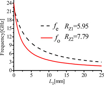
It is concluded that the proposed resonator is dual-mode with f 0 < f e as shown in Fig. 2.
Characteristics of SLSIR with varied L 1. Associated parameters: L 2 = 1.8, L 3 = 2, w 1 = 0.4, w 2 = 5.8, and w 3 = 0.2 (all in mm).

By taking f e to be the first spurious resonant frequency and f 0 to be the fundamental resonant frequency, then
 $$\displaystyle{{{f_e}} \over {{f_0}}} = \displaystyle{{{\theta _e}} \over {{\theta _0}}},$$
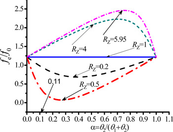
where θ e and θ 0 represent the electrical lengths of even-and odd-mode resonant frequencies, respectively. Several solutions for θ 1 and θ 2 are dependent on the choice of both impedance ratio R Z1 and electrical length ratio α = θ 2/(θ 1 + θ 2). Figure 3 shows the normalized ratio f e /f 0 for the SLSIR with R Z1 = 5.95 and R Z2 = 7.79. Let f 0 = 2.4 GHz and f e = 3.5 GHz (f e /f 0 = 1.46) with R Z1 = 5.95, the length ratio can be explicitly determined as 0.11. In this work, α = 0.11(θ 1 = 87.9° and θ 2 = 10°) and R Z1 = 5.95(Z 1 = 87.5 Ω and Z 2 = 14.71 Ω) are chosen for generating the dual-band frequency responses.
Normalized ratio f e /f 0 for the SLSIR with R Z1 = 5.95.

B. Design of the dual-band BPF
Based on the above analysis, the proposed filter, shown in Fig. 4(a) is designed with respect to the coupling schematic topology shown in Fig. 4(b). It is composed of two coupled half-wavelength SLSIRs with two cross-slots and two bended coupling feed lines.
(a) Layout and (b) coupling schematic topology of the proposed dual-band BPF.

The proposed filter is designed to have f
1 = 2.4 GHz and f
2 = 3.5 GHz with 3-dB fractional bandwidths of 8.3 and 6.4%, respectively. The element values of the prototype filter are g
0 = 1, g
1 = 0.9905, g
2 = 1.8219, J
1 = −0.5578, and J
2 = 1.6369. Based on the coupling theory according to the standard design procedure given in [Reference Hong18], the coupling matrixes
 ${\rm M}_{ij}^{{f_{_1}}} $
and
 ${\rm M}_{ij}^{{f_{_2}}} $
of the dual-band BPF are derived as follows:
 $$\eqalign{{\rm M}_{ij}^{{f_{_1}}} & = \left[ {\matrix{ {{\rm M}{}_{SS}} & {{\rm M}{}_{S1}} & {{\rm M}{}_{S2}} & {{\rm M}{}_{SL}} \cr {{\rm M}{}_{1S}} & {{\rm M}{}_{11}} & {{\rm M}{}_{12}} & {{\rm M}{}_{1L}} \cr {{\rm M}{}_{2S}} & {{\rm M}{}_{21}} & {{\rm M}{}_{22}} & {{\rm M}{}_{2L}} \cr {{\rm M}{}_{LS}} & {{\rm M}{}_{L1}} & {{\rm M}{}_{L2}} & {{\rm M}{}_{LL}} \cr}} \right] \cr & = \left[ {\matrix{ 0 & {0.062} & 0 & { - 0.047} \cr {0.062} & 0 & {0.0746} & 0 \cr 0 & {0.0746} & 0 & {0.062} \cr { - 0.047} & 0 & {0.062} & 0 \cr}} \right]\,\,{\rm for}\,2.4\,{\rm GHz,}}$$
 $$\eqalign{{\rm M}_{ij}^{{f_{_2}}} & = \left[ {\matrix{ {{\rm M}{}_{SS}} & {{\rm M}{}_{S1}} & {{\rm M}{}_{S2}} & {{\rm M}{}_{SL}} \cr {{\rm M}{}_{1S}} & {{\rm M}{}_{11}} & {{\rm M}{}_{12}} & {{\rm M}{}_{1L}} \cr {{\rm M}{}_{2S}} & {{\rm M}{}_{21}} & {{\rm M}{}_{22}} & {{\rm M}{}_{2L}} \cr {{\rm M}{}_{LS}} & {{\rm M}{}_{L1}} & {{\rm M}{}_{L2}} & {{\rm M}{}_{LL}} \cr}} \right] \cr & = \left[ {\matrix{ 0 & {0.05} & 0 & { - 0.036} \cr {0.05} & 0 & {0.0575} & 0 \cr 0 & {0.0575} & 0 & {0.05} \cr { - 0.036} & 0 & {0.05} & 0 \cr}} \right]\,\,{\rm for\, 3}.{\rm 5}{\rm} \,{\rm GHz,}}$$
where M
ij
is the coupling coefficient of M
12 = FBW · J
2/g
2, M
SL
= FBW · J
1/g
1 and
 ${M_{S1}} = {M_{2L}} = {{FBW} / {\sqrt {{g_1}{g_2}}}}.$
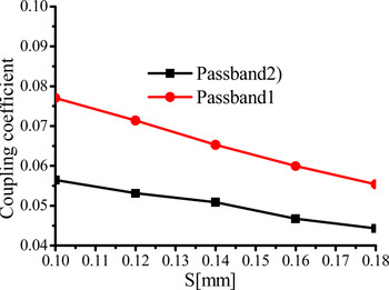
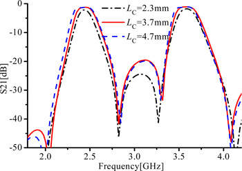
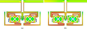
Figure 5 shows the variation of coupling coefficient M ij with regard to different values of coupling space (S) between two resonators. The coupling coefficient (M 12) for the first passband (2.4 GHz) and second passband (3.5 GHz) are as a function of the gap S. It should be noted that the coupling coefficient (M SL ) between source and load is very small as compared to the coupling coefficient M 12, thus M SL would not affect the characteristics of two passbands as described in [Reference Chang, Kao, Weng and Yang19]. As it can be seen in Fig. 5, the coupling coefficient of both passbands decreases as the spacing S increases. When the spacing of S is larger, the weaker the coupling leads to mode splitting. The small spacing S makes proper coupling for the two passbands. As shown in Fig. 6, the bandwidths of the lower and upper passbands are a function of parameter L C . Both bandwidths are changed when the parameter L C is varied. To satisfy the desired bandwidths of the first and second passbands, the coupling spacing S and the parameter L C are chosen to be S = 0.1 mm and L C = 3.7 mm, respectively. Figure 7 shows the current distributions of the proposed filter at 2.4 and 3.5 GHz. Through the plots, we can conclude that the EM waves are transmitted in the filter from port1 to port2.
Coupling coefficient with varied coupling space S.

Simulated results with varied L C .

Current distributions of the proposed filter at 2.4 and 3.5 GHz.

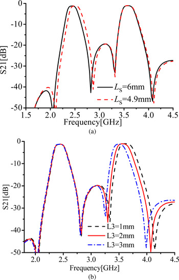
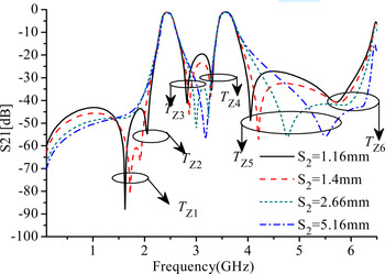
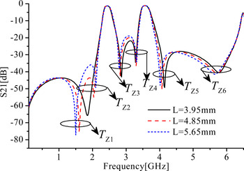
In this paper, two cross-slots and open stubs are introduced to SIR. As shown in Fig. 8(a), the variation of L S can tune the first passband, while the second passband is tuned by varying the length of L 3 as shown in Fig. 8(b). As illustrated in Figs 9 and 10, source–load coupling method is used to create six transmission zeros. Transmission zeros T Z2 and T Z3 around the first passband are generated according to the coupling matrix defined in (8), whereas transmission zeros T Z4 and T Z5 around the second passband are generated according to the coupling matrix defined in (9). The extra pair of transmission zeros T Z1 and T Z6 can be created due to the parameters L and S 2. As it can be seen in Fig. 10, the extra transmission zero T Z1 in lower stopband occurred at the frequencies where the corresponding distance (L) from the feed point to the right-angle bended coupling line is equivalent to quarter-wavelength of the lower frequency, while the extra transmission zero T Z6 may be produced in upper stopband owing to the source–load coupling as illustrated in Fig. 9. These extra transmission zeros can help the rejection of signal and hence increase the out-of-band rejection. As it can be seen in Fig. 9, all transmission zeros can be removed by increasing the space (S 2) between source and load from 1.16 mm.
EM simulated results with varied: (a) L S and (b) L 3.

EM simulated results with varied S 2.

EM simulated results with varied L.

RESULTS AND DISCUSSION
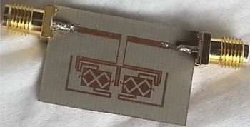
An experimental frequency dual-band BPF is built on a 0.508 mm Taconic RF-35(tm) substrate with relative dielectric of 3.5 and loss tangent of 0.0018. The simulation was carried out using EM simulation software IE3D, I/O ports were ordinary 50 Ω ports and coaxial connectors were not included. The measurement was performed using a scalar network analyzer. The prototype photograph of the proposed filter is shown in Fig. 11.
Prototype photograph of the proposed dual-band bandpass filter.

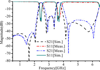
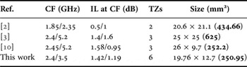
Simulated and measured results of the proposed dual-band BPF is shown in Fig. 12. The physical dimensions (unit: mm) of the dual-band BPF are summarized as follows: l 1 = 17.6, l 2 = 1.8, l 3 = 2, l = 4.55, l C = 3.7, w = 1.15, w 1 = 0.4, w 2 = 5.8, w 3 = 0.2, w 4 = 0.3, w 5 = 0.22, S = S 1 = 0.1, and S 2 = 1.16. The measured results are centered at 2.44/3.56 GHz with 3-dB fractional bandwidths of the 9.6/7.7%, respectively. The insertion losses of passbands, includes the losses from SMA connectors, are less than 1.4/1.2 dB, respectively and the return losses are better than 25/20.1 dB, respectively. In addition, transmission zeros due to the source-load coupling and symmetrical coupling between two SLSIRs can be found at 1.44/2/2.91/3.3/4.3/6.07 GHz. The lower and upper stopband rejections are greater than 40 and 20 dB, respectively. Stopband rejection between two passbands is better than 20 dB. Some discrepancies observed in passbands are mainly attributed to the possible tolerance in fabrication and implementation. Besides, the fabrication filter has the merit of a compact size of 19.76 × 12.7 mm2. Table 1 gives a performance comparison of the proposed filter with the other reported works. As it can be seen, the proposed dual-band BPF using SLSIR exhibits a compact size. It presents 42.2, 0.05, and 59.8% size reduction as compared with [Reference Wu, Liang, Qin and Lin2, Reference Chu and Chen3, Reference Chen, Chu, Li and Wu10], respectively. Good middle stopband rejection between first and second passbands, and upper stopband from 4.5 to 6.2 GHz are achieved due to the six transmission zeros which represent the major characteristic of this work as compared to the previous works such as [Reference Wu, Liang, Qin and Lin2, Reference Chu and Chen3, Reference Chen, Chu, Li and Wu10].
EM simulated and measured results of the dual-band bandpass filter.

Performance comparison with the reported works

CF, center frequency; IL, insertion loss; TZs, transmission zeros.
CONCLUSION
A dual-band BPF based on SLSIR is presented. The filter is constructed using two coupled half-wavelength SLSIR with a pair bended coupling feed lines. Even- and odd-mode equivalent circuits of SLSIR are analyzed and design equations are derived for guiding the design of the device. The open stub and cross-slots are employed to fix the center frequencies at the desired location. The two central frequencies are located at 2.44/3.56 GHz. Six Transmission zeros are created to improve passbands isolation and stopband performance. The fabricated filter is compact with a size of 19.76 × 12.7 mm2 (0.274 × 0.176λ g , where λ g is the guided wavelength at the lower center frequency). Both passbands and stopbands of the dual-band filter were quite favorable. The proposed filter exhibits properties in terms of compact size and wide stopband. The measured and simulated results agree well.
ACKNOWLEDGEMENTS
The work for this grant was supported by National Natural Science Foundation of China (Grant no 61271026), by National Natural Science Foundation of China-NSAF (Grant no 10976005), by the Program for New Century Excellent Talents in University (Grant no NCET-11-0066), by the Research Fund of Shanghai Academy of Spaceflight Technology (Grant no SAST201243), and by the project (Grant no IRT1113) under “Program for Changjiang Scholars and Innovation Team in University”.
 Bukuru Denis received the M.S. degree in electromagnetic field and microwave technology from the University of Electronic Science and Technology of China (UESTC) in 2013, and is now pursing his Ph.D. degree in electromagnetic field and microwave technology at the University of Electronic Science and Technology of China (UESTC), Chengdu, China, from 2013. His research interests include microwave/millimeter-wave devices, circuits, and systems.
 Kaijun Song (M'09–SM'12) received the M.S. degree in radio physics and the Ph.D. degree in electromagnetic field and microwave technology from the University of Electronic Science and Technology of China (UESTC), Chengdu, China, in 2005 and 2007, respectively. Since 2007, he has been with the EHF Key Laboratory of Science, School of Electronic Engineering, UESTC, where he is currently a full Professor. From 2007 to 2008, he was a postdoctoral research fellow with the Montana Tech of the University of Montana, Butte, USA, working on microwave/millimeter-wave circuits and microwave remote sensing technology. From 2008 to 2010, he was a research fellow with the State Key Laboratory of Millimeter Waves of China, Department of Electronic Engineering, City University of Hong Kong, on microwave/millimeter-wave power-combining technology and Ultra-Wideband (UWB) circuits. He was a senior visiting scholar with the State Key Laboratory of Millimeter Waves of China, Department of Electronic Engineering, City University of Hong Kong in November 2012. He has published more than 80 internationally refereed journal papers. His current research fields include microwave and millimeter-wave/THz power-combining technology; UWB circuits and technologies; microwave /millimeter-wave devices, circuits and systems; and microwave remote sensing technologies. Professor Song is the Reviewer of tens of international journals, including IEEE Transactions and IEEE Letters.
 Fan Zhang was born in Hunan, China, in 1989. He received the B.S. degree from the Hefei University of Technology, Hefei, China, in 2012. He is currently working toward the Ph.D. degree in the School of Electronic Engineering, University of Electronic Science and Technology of China, Chengdu, China. His research interests are microwave/millimeter-wave passive structure, including filters and power dividers/combiners. He is also involved in the investigation of quasi-optical beam-shaping techniques, diffractive optics, and reflector design.