INTRODUCTION
Recently, we have described the quantum model for the subatomic confinement (Berec, Reference Berec2012) of the proton beam, which is channeled along the axial <100> axis of a silicon nanocrystal. By measuring the transverse projection of electron densities inside nanocrystal, we have analyzed the cross-section for the process of proton induced X-ray emission with MeV proton energies as a function of the proton impact parameters. We obtained values for the proton beam peak half-width, which have shown smaller diameter in comparison to size of the Bohr radius, i.e., the average radius of a hydrogen atom in its ground state. The effect of super-focusing of ions induced by channeling through thin crystals with less than 100 nm thicknesses was generated using the model of cylindrically-symmetric and harmonic continuum proton-crystal interaction potential (Gemmell, Reference Gemmell1974).
In this paper, for the first time, we demonstrate that the full three-dimensional structure of a single atomic orbital (Zuo et al., Reference Zuo, Kim, O'Keeffe and Spence1999) can be imaged by using the high harmonics generated from intense picosecond proton pulses focused relative to low index axial axis of a silicon nanocrystal. The model is based on the “hyperchanneling effect” of protons (Gemmell, Reference Gemmell1974), corresponding to Appleton et al. (Reference Appleton, Moak, Noggle and Barrett1972) who presented the angular phase space projections in the axial hyperchanneling regime, and it is in conjunction to recent experimental investigation obtained for ultra-thin silicon crystal (Motapothula et al., Reference Motapothula, Dang, Venkatesan, Breese, Rana and Osman2012a; Reference Motapothula, Dang, Venkatesan, Breese, Rana and Osman2012b).
The hyperchanneling effect characterizes the harmonic and is highly correlated to trajectories of swift ions (protons), which incident upon a crystal parallel to its small index symmetry axes, exhibits a series of soft small-angle scatterings that preserve the motion between the lattice rows. Namely, when charged particles enter the nanocrystal channel they produce a transverse kinetic energy determined by the potential at their point of entry and the incident angle (φ). Consequently, the region where a particle (ion, proton) can be sampled is determined by the condition that the net continuum potential at any point r in the transverse plane (U(r)), has to be smaller than the ion transverse energy (E ⊥), i.e., the particle trajectory is restricted to that portion of the transverse plane (A(E ⊥)) where U(r) ≤ E ⊥. Conversely, the ion channeling transmission is strictly defined for the state: U(r) > E ⊥. The remainder of this paper deals with specific solutions of the area of the available space: A(E ⊥) = A(r, E, φ), attainable for different conditions of well channeled transmitted protons where the proton beam is perfectly collimated and relative to Si nanocrystal low index axis, occupying the radius of the channel center that is comparable to size of the Bohr radius.
Here we present the principal study based on numerical modeling and real atomistic simulation model performed by a well-known and used FLUX code (Smulders & Boerma, 1987), which describe the beam transmission of proton electromagnetic field in the nanocrystalline medium, incorporating the feedback of electron densities under intense laser pulses. Numerically, Monte Carlo code FLUX during the initialization stage assigns precursor position of coordinates over the transverse plane as random distributed for an incoming beam, so that each particle can be initialized with equal probability in its accessible region; as a result the flux redistribution is calculated as a function of the angle of incidence for every point in the channel. The sizes of a bin along the x and y axes of the channel are equal to 0.005 nm. The ions backscattered from a foreign atom located (inserted) in the center of a channel will have a maximum of flux enhancement for perfect alignment (φ = 0) that will decrease with increasing φ as the flux distributions approaches the random value.
In contrary to “standard” flux peaking effect (Kumakhov, Reference Kumakhov1972a; Reference Kumakhov1972b), which refers to spatial focusing of channeled particles in the center of the channel (axial/planar) at λ/4 oscillation wavelength where the flux enhancement reaches only few times compared to a random level in the unit cell, the qualitatively different effect, which is specific for axial channeling, called the super-focusing effect (Demkov & Meyer, Reference Demkov and Meyer2004) predicts that the flux density can reach a thousand times higher value than the initial flux outside of the lattice. In particular, full width at half maximum (FWHM) of the super-focused peak is much smaller than the thermal vibration amplitude (ρth = 0.0078 nm) of the silicon lattice atoms.
However, the phenomena of axial peak-focusing was not fully explained until Demkov and Meyer (Reference Demkov and Meyer2004) performed quantum mechanical model calculations in the transverse phase space of axial channels and revisited the flux peaking effect studies. In their theoretical study, it was predicted to appearance extremely narrow, less than 0.005 nm focusing region of a highly collimated 1 MeV proton beam inside the <001> silicon channel. The study was based on the continuum proton-silicon interaction potential, dominantly cylindrically symmetric and harmonic. Assuming the calculated flux density value is sensitive to the accurate potential model, they applied Hartree-Fock approximation. The estimated FWHM of the proton beam at the super-focusing point is about 11 times smaller than the Bohr radius (0.0529 nm), i.e., the super-focusing region is less than 0.0048 nm, while the total length of the focusing region is about 17.2 nm. In another words, it was found that beyond the possibility to locate the atom (impurity) like in standard flux peaking effect, in the case of axial flux super-focusing one can probe interior subatomic structure of a target atom.
Taking into account that the super-focused regions are pm-sized spots, until now, experimental capture of perfectly collimated beams, originating from the super-focusing, at the exit of the crystal was difficult. Very recently Motapothula et al. (Reference Motapothula, Dang, Venkatesan, Breese, Rana and Osman2012a; Reference Motapothula, Dang, Venkatesan, Breese, Rana and Osman2012b; Motapothula, Reference Motapothula2013) demonstrated successful experimental observation of those super-focused channeled proton angular distributions in transmission regime and found excellent agreement with corresponding simulations, providing the proof for super-focusing effect existence. They captured the exit angular distributions in range from 500 keV to 2 MeV energy for protons via the 55 nm [001] silicon membrane using the special technique of high-resolution ion channeling, new fabrication procedure (Dang et al., 2013) to create ultra-thin crystal that allows uniform thickness over the entire surface, and nuclear microprobe to perform experiments on such membranes.
In our high-resolution proton scattering, we have established a hyperchanneling regime at 4 K for the proton beam and a silicon nanocrystal as the target, allowing the super-focused protons to generate a nanolaser beam scans of the interior of a foreign atom that is a part of the silicon nanolattice (Pavesi & Lockwood, Reference Pavesi and Lockwood2004; Liang & Bowers, Reference Liang and Bowers2010). We have used the combination of low excitation intensity, 3 and 3.5 MeV initial proton energy and the proton beam incident angles in range from zero up to 20% of the critical angle for channeling (Lindhard, Reference Lindhard1965).
THEORETICAL AND EXPERIMENTAL MODEL
In this section, a general description of the experimental procedure and the simulation parameters are given. To describe inner-shell ionization and excitation of atoms as a function of the impact parameter (Gemmell, Reference Gemmell1974; Appleton et al., Reference Appleton, Moak, Noggle and Barrett1972), we have applied semi-classical method of the coupled-channel calculations (Bransden et al., Reference Bransden, McCarthy, Mitroy and Stelbovics1985; Thompson, Reference Thompson1988), where the projectile following a classical trajectory provides a time-dependent electrostatic perturbation on the target electrons. A set of first-order ordinary coupled differential equations for the coefficients originating from the expansion of Molière approximation of the Thomas-Fermi interaction potential (Lindhard, Reference Lindhard1965; Gemmell, Reference Gemmell1974), the so-called coupled-channel equations, were numerically integrated along the classical trajectory of the projectile (proton) for a given impact parameters φx and φy that are the x − y components of the proton scattering angle. The channeled proton distributions are double-mapped in the phase space: first in the coordination plane, x′ − y′, then in the scattering-angle plane, ϑx − θy (Berec, Reference Berec2012), in accordance with chosen value of the crystal thickness, L and the tilt angle (φ). Nanocrystal potential between two i and j lattice sites is
 $$\Phi _{i\comma j}={\rm }U_i \lpar r\rpar +\displaystyle{B \over {r_{ij} ^n }}\comma \;$$
where n denotes the Born exponent, and coefficients B and n are experimentally obtained from the ion compressibility fitting parameters (Kittel, Reference Kittel1995). Degree of the confinement field (C) and discretized energy (ε), respectively, are
 $$C=\left({1{\rm+}{{{\rm \omega} _e } / \Omega }} \right)^{{1 \over 2}} s\comma \; {\rm \varepsilon}=\left({{s / a}} \right)f_r \hbar {\rm \omega} _e \comma \;$$
where ωe = (4πe 2n e/m e)1/2 is the angular frequency of the oscillations of the electron gas induced by the proton (Krause et al., Reference Krause, Barrett, Datz, Dittner, Jones, Gomez and Vane1994; Reference Krause and Datz1996), a = a 0[9π2/(128Z 2)]1/3 is the screening radius of the atom, with s being the distance from local stability point in the harmonic continuum potential (Lindhard, Reference Lindhard1965; Gemmell, Reference Gemmell1974), and a 0 = 52.9 pm is the Bohr radius (Krause et al., Reference Krause, Barrett, Datz, Dittner, Jones, Gomez and Vane1994), f r is the average frequency of transverse proton motion close to the channel axis and ħ is the reduced Planck constant. Dispersions of the components of the proton scattering angle are Ωx2 = Ωy2 = Ω2/2. Details of the atomic orbital coupled-channel calculations may be found elsewhere (Thompson, Reference Thompson1988).
When a high-intensity laser pulse interacts with collective electron plasma excitations in solid target, a several tens of percent of the plasma electrons in the vicinity of the laser focus can be effectively accelerated, forming a directed stream of electrons due to electrostatic fields which arise from the ponderomotive expulsion of plasma electrons from regions of high laser intensities. The acceleration process occurs within the laser pulse duration only. To obtain much stronger acceleration at the sharp density interface on the back of the nanocrystal target than on the front, we consider the proton beam energy transferred under T = 4 K to the silicon nanocrystal target (150 nm in diameter multiplied by 100 nm thickness). The induced transfer of the hot electron mean energy E = 0.7 MeV/nm is superimposed to channeled proton field, which is relative to specific nanocrystal tilts (in range: 0–20% of the critical angle for channeling), providing the transverse projection of electron density of states (DOS) that allows tomographic reconstruction of the highest occupied atomic orbital of host silicon. Such nanoscale precision scanning technique is based on dynamical analysis of an electron wave packet by creating a highly resolved image in real conditions with produced detailed map of discrete inter-atom positions (Berec, Reference Berec2012).
Recently (Dang et al., Reference Dang, Motapothula, Ow, Venkatesan, Breese, Rana and Osman2011; Motapothula et al., Reference Motapothula, Dang, Venkatesan, Breese, Rana and Osman2012a) performed standard axial ion channeling experiment in perfectly, crystalline, nm-thick silicon membrane close to conditions treated here, confirming the strong reduction of multiple scattering effects for ultra-thin targets in range up to 100 nm. They showed even better resolution in experimentally obtained channeled patterns in comparison to the same obtained with FLUX simulation using Ziegler-Biersack-Littmark Universal interaction potential.
Similarly to the former study, we have performed a numerical probe using FLUX code, but unlike to Dang et al. (Reference Dang, Motapothula, Ow, Venkatesan, Breese, Rana and Osman2011) and Motapothula et al. (Reference Motapothula, Dang, Venkatesan, Breese, Rana and Osman2012a; Reference Motapothula, Dang, Venkatesan, Breese, Rana and Osman2012b) we used the Thomas-Fermi-Molière interaction potential corresponding to “proper” axial channeling (Lindhard, Reference Lindhard1965), i.e., the hyperchanneling — attainable for zero degree proton beam alignment toward <111> silicon axis, including the tilt angles of the proton beam: φ = 0.05ψc, φ = 0.10ψc, φ = 0.15ψc and φ = 0.20ψc for nanocrystal thickness of L = 100 nm.
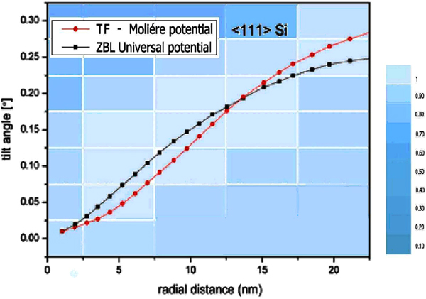
In order to illustrate dominance and spatial confinement effect of the above potentials at various channel points we have compared the influences of the TMF - interaction potential and the Ziegler-Biersack-Littmark Universal potential inside <111> silicon channel area considering different radial atomic distances and gradual change of the tilt angle (with step 0.05°) as given in Figure 1. Marked points designate the <111> channel area where the corresponding potentials exhibit the strongest confinement effect following the tilt.
Influences of the Thomas-Fermi-Molière interaction potential (red circles) and Ziegler-Biersack-Littmark Universal interaction potential (black circles) of the perfectly collimated proton beam, taken for <111> axial channel of 100 nm thick silicon, according to different radial distances from the atomic strings (lying on three nearest square coordination lines of the <111> axial channel) and various tilt angles. Bright areas (intensities are shown in normalized color scale) show the channel area where the corresponding potentials exhibit the strongest confinement effect.

In the former analysis, as well to demonstrate how the bound-state wave-packet motion appears in the harmonic spectra we use the Thomas-Fermi proton-atom interaction potential in the Moliére approximation (Gemmell, Reference Gemmell1974) in the following form:
 $$V\lpar r^{\prime}\rpar =\displaystyle{{Z_1 Z_2 e^2 } \over {r^{\prime}}}\left[\matrix{0.35\exp \lpar \!\!-\! br^{\prime}\rpar \cr + 0.55\exp \lpar \!\!-\! 4br^{\prime}\rpar \cr +0.10\exp \lpar \!\!-\! 20br^{\prime}\rpar} \right]\comma \;$$
where Z 1 and Z 2 are the atomic numbers of the hydrogen and silicon atoms, respectively, e is the elementary charge, r′ is the distance between the proton and atom, b = 0.3/a. By varying the initial tilts of the proton beam, we performed a numerical pump-probe measurement of the electron wave-packet motion (Berec, Reference Berec2012). We further applied the continuum approximation (Lindhard, Reference Lindhard1965; Gemmell, Reference Gemmell1974),
 $$U_i^{th} \lpar x\comma \; y\rpar =U_i \lpar x\comma \; y\rpar +\displaystyle{{{\rm \sigma} _{th}^2 } \over 2}\left[{\partial _{xx} U_i \lpar x\comma \; y\rpar +\partial _{yy} U_i \lpar x\comma \; y\rpar } \right]\comma \;$$
where U i(x, y) is the continuum interaction potential of the proton and ith atomic string, which includes the effect of thermal vibrations. σth is the one-dimensional thermal vibration amplitude of the atoms.
ENERGY LOSS
The energy loss of the proton in the channel is taken into account via relation
 $$- \displaystyle{{dE} \over {dz}}=\displaystyle{{4{\rm \pi} Z_1^2 e^4 } \over {m_e v^2 }}n_e \ln \displaystyle{{2m_e v^2 } \over {\hbar {\rm \omega} _e }}\comma \;$$
where m e is the electron mass, v the proton velocity, n e = ΔU th/4π is the density of the crystal's electron gas averaged along the z axis, Δ = ∂xx + ∂yy, ΔU th is continuum potential of the crystal. In the MeV regime, the main contribution to the energy loss comes from inelastic interactions with electrons (Smolders & Boerma, Reference Smolders and Boerma1987). We have followed the study of Appleton et al. (Reference Appleton, Erginsoy and Gibson1967) who confirmed experimentally and numerically that K-shell excitation in silicon (in case of well channeled protons 3–11 MeV) can be neglected, while the energy loss due to ionization of the L shell electrons is greatly reduced (90%) for the best channeled protons in the (111) direction in silicon, keeping in mind that maximal impact parameter, b max, is about 1.6  ${\dot {\rm A}}$. Former results imply that energy loss in particular can be fully attributed to the interaction of channeled protons with the valence electrons treated as a Fermi gas (Gemmell, Reference Gemmell1974). Hence, if one assumes the approach from Pines (Reference Pines1964), the energy loss due to valence electrons can be separated by two contributions coming from collective (plasma) excitations and the single particle excitations, that is:
 $$- \left({\displaystyle{{dE} \over {dz}}} \right)_{val}=\displaystyle{{4{\rm \pi} Z_1 ^2 e^4 } \over {m_e v^2 }}N\left({Z_{val} \ln \displaystyle{v \over {v_F }}+Z_{loc} \ln \displaystyle{{2m_e vv_F } \over {\hbar {\rm \omega} _p }}} \right)\comma \;$$
where v F is the Fermi velocity of the valence electron gas, v is the channeled particle velocity, N Z val and N Z loc are effective electron densities for plasma and single-particle excitations, respectively, ωp denotes the electron plasma frequency defined in presented Eq. (5) as ωe = (4πe 2n e/m e)1/2. Experimental measurement in silicon (Appleton et al., Reference Appleton, Erginsoy and Gibson1967), which we followed, confirmed that the local electron density sampled by the hyperchanneled proton approximately equals to the valence electron gas density, i.e., Z loc ≈ Z val. Former equation, after the substitution of Z loc ≈ Z val = Z, reduces exactly to Eq. (5) where n e = NZ is density of electron gas, coinciding with the Lindhard (Reference Lindhard1965) and Winter expression (Gemmell, Reference Gemmell1974). The specific change of the dispersion of the proton scattering angle Gemmell (Reference Gemmell1974) caused by its collisions with the electrons is included in the form
 $$\displaystyle{{d\Omega ^2 } \over {dz}}=\displaystyle{{m_e } \over {m_p^2 v^2 }}\left({ - \displaystyle{{dE} \over {dz}}} \right)\comma \;$$
where m p denotes the proton mass.
Note that we have taken into account experimentally confirmed fact that the energy loss of MeV channeled particle (especially at large impact parameters) exhibits quit weak contribution of collisions of the incident ion with nuclei of the lattice, and as a result enfeeble effect to the temperature dependence of the sample (Gemmell, Reference Gemmell1974 and reference therein), which means that the effect of energy loss in the MeV hyperchanneling regime cannot destroy the sample. This is in agreement with series of recent experimental studies (Dang et al., Reference Dang, Motapothula, Ow, Venkatesan, Breese, Rana and Osman2011; Motapothula et al., Reference Motapothula, Dang, Venkatesan, Breese, Rana and Osman2012a), which could not be performed otherwise. Former peculiarity strongly holds even in the case of dechanneling. In turn, such property is also in agreement with the results that the maximum range does not change with the temperature (Fujimoto et al., Reference Fujimoto, Komaki, Ozawa, Mannami and Sakurai1969). It is important to note that the energy loss represents a function of distance of penetration. It changes per unit length, reaching the maximum close to end of range. According to Tavernier (Reference Tavernier2010 and references therein), range for 2 MeV protons in silicon is about 50 µm, which is much more than the length of silicon sample considered in our study.
Obtained hyperchanneled Gaussian distributions were rescaled around the singularities (for reduced thickness of Λ = 0.25) providing the reduction of the noise accumulation with order: O(N − 1/2), where N is the count statistic of the proper channeled (Lindhard, Reference Lindhard1965), proton trajectories.
The analysis of the proton scattering process in question is carried out via the mapping of the impact parameter plane to the transverse position plane (Berec, Reference Berec2012; Gemmell, Reference Gemmell1974), in accordance with the chosen values of φ and the crystal thickness L. The corresponding reduced crystal thickness is Λ = f r L/v 0 where f r = 5.94 × 10¹³ Hz and v 0 is the initial proton velocity. The nonlinear map J r(x, y, φ, Λ) transforms the original phase space point (x, y) into the phase space point where the projection is measured. The solution is expressed as
 $$J_r \lpar x\comma \; y\comma \; {\rm \varphi}\comma \; \Lambda \rpar =\displaystyle{{\partial x^{\prime}} \over {\partial x}}\displaystyle{{\partial y^{\prime}} \over {\partial y}} - \displaystyle{{\partial x^{\prime}} \over {\partial y}}\displaystyle{{\partial y^{\prime}} \over {\partial x}}\comma \;$$
where x and y are the components of the proton impact parameter, i.e., the components of its initial position in the transverse position plane. Thus, equation J r(x, y, φ, Λ) = 0 determines the lines in the impact parameter plane along which the proton yield is singular.
Quantum Monte-Carlo simulations of the elastic scattering trajectories are combined with coupled channel calculations to describe inner-shell ionization and excitation as a function of impact parameter. The initial proton energy E 0 is 3 MeV and the crystal thickness, L, is changed from 66.1 nm to 100 nm. The temperature was set to 4 K in order to reduce the thermal vibration of the lattice. The proton beam incident angle is varied in the range between 0 and 0.20ψc, where ψc = [2Z 1Z 2e 2/(dE 0)]1/2 = 6.09 mrad is the critical angle for channeling, with dbeing the distance between the crystal's atoms within the atomic strings (Kittel, Reference Kittel1995; Bransden et al., Reference Bransden, McCarthy, Mitroy and Stelbovics1985). The one-dimensional thermal vibration amplitude of the atoms is σth = 7.4 pm (Batterman & Chipman, Reference Batterman and Chipman1962; Slater, Reference Slater1964). Binary collisions are included for each interaction using the momentum approximation, and channeled particle trajectory dependence on every atom in the chosen string is in-calculated besides the continuum potential contributions of the surrounding strings. The number of crystal's atomic strings defining the <111> channel is 36, i.e., the atomic strings lying on the three nearest square coordination lines (Kittel, Reference Kittel1995; Krause et al., Reference Krause, Barrett, Datz, Dittner, Jones, Gomez and Vane1994) are considered. The implicit Runge-Kutta method of the fourth order (Abramowitz & Stegun, Reference Abramowitz and Stegun1965; Parker & Chua, Reference Parker and Chua1989) is used to iterate the solutions of protons trajectories from the uniform distributions within the region of the channel. The components of the proton impact parameter, x and y, are mapped into single density matrix where the initial number of protons was set to 4 ×10⁷.
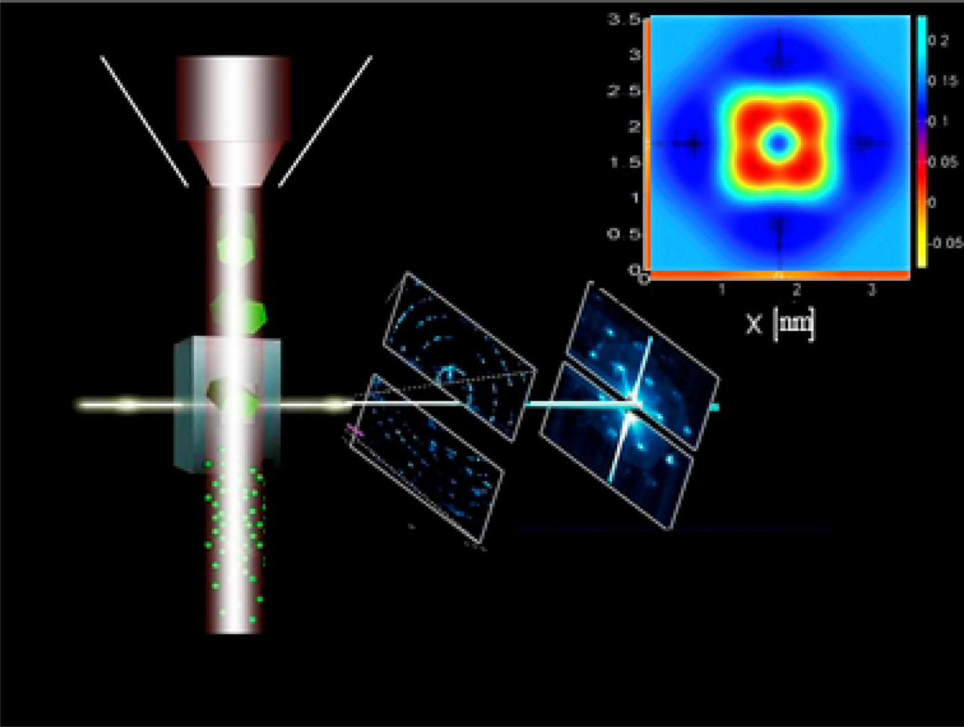
Laser system (represented schematically in Figs. 2 and 3) induces optimization of the potential barrier (in target) increasing it compared to the transverse energy E ⊥ of the channeled proton. As a result, the proton motion is additionally stabilized and supplementary confined in interatomic potential area located outside to valence electron distances (Barrett et al., Reference Barrett, Appleton, Noggle, Moak, Biggerstaff, Datz, Behrisch, Datz, Appleton and Moak1975), i.e., where the energy loss is anomalously low. Besides, by setting up the intense field at the rate close to a 0 = 1 au which binds over the Coulomb force — creating in such way the laser-dressed atoms, which are proved to be stable toward energy losses induced by ionization (Gavrila, Reference Gavrila2002), it is also possible to induce the atomic stabilization in target. Laser stabilization of atoms is a well-known and experimentally confirmed (Reiss, Reference Reiss2001), specific steady-state created under asymptotically high-frequency and high-intensity radiation field of constant amplitude, which prevents ionization of an atomic electron (Gavrila, Reference Gavrila2002). The intensities required to reach the stabilization regime are within standard tabletop amplified sub-picosecond laser systems, which can exceed 1018 W/cm2 for λ = 800 nm, as in case of conventional Ti: sapphire laser.
A schematic representation of the measurement setup: laser system (vertical) and perfectly collimated (perpendicular) proton beam. Right top corner: tomographic result of electron DOS obtained for the considered silicon nano-crystal target.

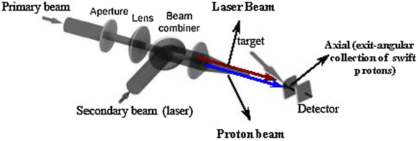
A schematic of the ‘‘standard’’ experimental setup, representing the main part of the beam-line focused with a spherical lens to the target position and exit plane axial collection of the swift protons, with a pierced mirror and a spherical lens on entrance of a fiber optic coupled with the detector. After passing the beam combiner, the laser beam (red) and the proton beam (blue) are spatially separated by the critical angle for <111> silicon: φ = ψc.

To model numerically a non-decaying bound states in the intense laser field, we have used full three-dimensional KH stabilization regime (van Druten et al., Reference van Druten, Constantinescu, Schins, Nieuwenhuize and Muller1997), where the KH potential are further expanded into a Fourier series
 $$V\left({r+{\rm \alpha} \left(t \right)} \right)=\sum\limits_n^{} {V_n \left({r\comma \; {\rm \theta}\semicolon \; {\rm \alpha} } \right)} {\rm }e^{in\left({{\rm \varphi} - {\rm \omega} t} \right)} \comma \;$$
where α = F 0/ω2 is the pulse amplitude, and θ and φ are the polar angles defining circular Coulomb potential in short-range approximation (Tikhonova et al., Reference Tikhonova, Volkova and Skurikhin2002). The maximum laser induced electric-field amplitude, E 0, corresponds for a Ti: sapphire laser (λ = 800 nm) to a peak intensity of ≈2.16 × 10¹⁸ Wcm−2, where an angular frequency of ħω = 27.21 eV is used as a standard value employed in studies of atomic stabilization.
The details of the channeling experimental setup, detection system, and a sample preparation are the same as those reported in Motapothula et al. (Reference Motapothula, Dang, Venkatesan, Breese, Rana and Osman2012a; Reference Motapothula, Dang, Venkatesan, Breese, Rana and Osman2012b); however the function and versatility of experimental setup are extended by a laser system. In Figure 3, a secondary collimated, laser-beam is deflected through the beam combiner and redirected toward target under small impact parameter (which corresponds to critical angle, ψc) close to atomic strings (in order to establish control over valence electron dynamics).
RESULTS
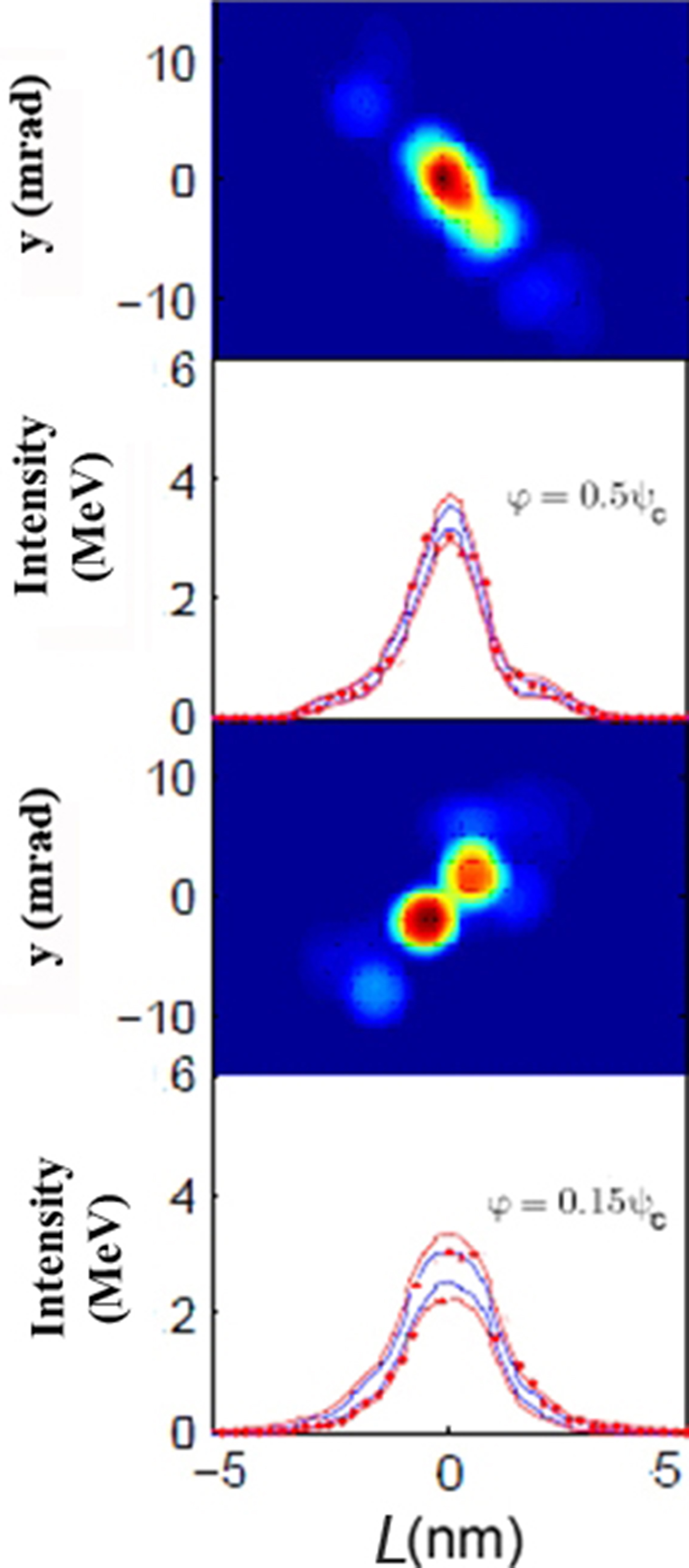
Figure 4 shows the tomographic reconstruction (in velocity phase space) of electron DOS for the highest occupied atomic orbital in the ±5 nm focal region inside the silicon nanocrystal core. The proton beam energies are 3 and 3.5 MeV, the incident angles are 0.05ψc and 0.15ψc, and the nanocrystal thickness is L = 100 nm. φ = 0.05ψc and 0.15ψc are the proton beam incident angles along the x (y) axis in the transverse position plane. At 3 and 3.5 MeV excitation intensity and the proton beam tilt angles (relative to <111> axis): 0.05ψc, the spectrum contains one maximum of a single broad transmission peak FWHM of 0.482 nm.
Proton beam intensity distribution in transverse position plane and the tomographic reconstruction of the highest occupied atomic orbital representing electron DOS in the 5 nm focal region inside the silicon nanocrystal core, obtained by the numerical probe. Here applied Thomas-Fermi-Molière interaction potential includes real data parameters: Debye thermal vibration amplitude (σth = 7.4 pm), exact Young's modulus which is largest along the <111> silicon axis (E = 187.5 GPa) and high mechanical quality factor of silicon (Q > 107). DOS along the x − y axis are obtained in the configuration phase space and velocity phase space for L = 100 nm thick silicon nanocrystal. Two-dimensional representation of channeled proton flux is shown for the proton beam incident angles: φ = 0.05ψc, 0.15ψc (the proton beam energies are 3 and 3.5 MeV) in the transverse position plane. The corresponding Gaussian fits are red colored.

The proton transmission through the silicon nanocrystal channel close to low index axis is accompanied with spontaneous emission of approximately 140 meV below the silicon band gap that is generally assigned to the recombination of the excitons (Liang & Bowers, 2005). The maximal enhancement in proton flux density corresponds to area inside the central equipotential curve, of axial crystal channel.
 $${\rm \gamma} \left({A_{l_0 } \lpar E_ \bot \rpar } \right)\approx \ln \left\vert {\displaystyle{{A_0\, k} \over {{\rm \pi} E{\rm \varphi} ^2 }}} \right\vert \comma \;$$
where γ(A l 0(E ⊥)) denotes effective potential area as a function of the incident proton beam transverse energy (Berec, Reference Berec2012; Lindhard, Reference Lindhard1965).
The results obtained for 3 and 3.5 MeV proton beam energies and tilt angle φ = 0.15ψc show the non-equilibrium DOS across the central part of the channel as a non-uniform flux redistribution. We can clearly see appearing of one central maximum as the sharply focused spot, followed by one asymmetrical pairs of lateral patterns due to strong perturbation of the harmonic potential in the channel. This implies the strong harmonic effect on the reversibility principle for the silicon nanocrystal, in the effective continuum interaction potential, even in vicinity of low index 〈111〉 axis where one would expect the uniform spectrum of transverse energy.
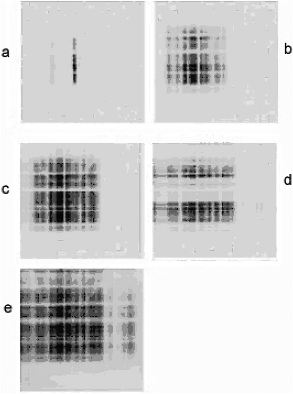
Figure 5 shows proton transmission patterns in the two-dimensional representation on the exit-scattering plane of the nanocrystal, which are obtained by mapping of positions in transversal position plane (Eq. (8)), for incident angles: ϕ = 0, 0.05ψc, 0.10ψc, 0.15ψc, and 0.20ψc, and thickness L = 100 nm. It is evident that for φ = 0, 0.05ψc, 0.10ψc, and 0.15ψc each of the distributions has one strong and narrow maximum, while for φ = 0.20ψc, proton distribution becomes broader, and fairly uniform. As the tilt angles decrease, the transmission pattern becomes narrower because of the preferential amplification of frequencies close to the maximum of the energy spectrum. It is also evident that for the values of the crystal tilt angle equal to φ = 0.15, spatial distribution structure exhibits characteristic splitting in two partitions, along horizontal axis, this is accompanied by a strong rearrangement and decrease in the proton flux. Thus, as the tilt angle decreases, the spatial distributions approach to the center of the channel, accompanied with maximum value of the channeled protons yield, for the zero-degree tilt angle. From the results in Figure 4, one can determine a quantitative correlation between the maximal value of the channeled protons yield (flux) and the super-focusing effect. The increase in crystal tilts magnitude relative to 15%, leads to annihilation of the super-focusing effect, i.e., the patterns become broader, inhomogeneous, with low peak intensity. One can clearly see the resolution precision in measurement of the electron density within the foreign atom as a function of the proton impact parameters. Such scanning probe method of the interior of the foreign atom allows the subatomic microscopy.
Numerically obtained transmission patterns in the exit — scattering-angle plane of 100 nm thick silicon nanocrystal. The ion beam divergence is set to 0.1 mrad. Two-dimensional representation of the hyperchanneled proton trajectories evolution with incident angles: (a) φ = 0, (b) φ = 0.05ψc, (c) φ = 0.10ψc, (d) φ = 0.15ψc, and (e) φ = 0.20ψc, corresponding to nanocrystal thickness of L = 100 nm, are mapped from the transverse position plane (according to Eq. (8)).

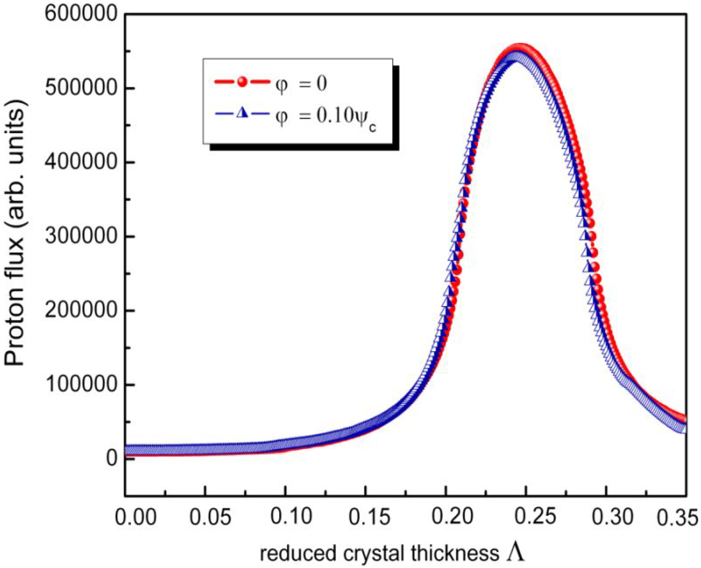
Figure 6 gives the resolution of the proton beam focusing spot. It shows channeled protons flux evolution with the reduced crystal thickness parameter Λ (between 0 and 0.3) in the focusing region inside the Bohr radius, around the centers of their spatial distributions, for φ = 0 and 0.10ψc. A full discussion of the reduced thickness is presented elsewhere (Krause et al., Reference Krause, Barrett, Datz, Dittner, Jones, Gomez and Vane1994; Reference Krause, Datz, Dittner, Gomez, Miller, Moak, Nešković and Pepmiller1986; Motapothula, Reference Motapothula2013). The full-widths of the two maxima are 0.044 and 0.043, respectively, and the corresponding values of ΔL are 27.8 and 27.5 nm, respectively. The small downward shifts from the super-focusing point at φ = 0 are attributed to small perturbation induced via harmonic component of the continuum proton-crystal interaction potential. Taking into account lattice thermal vibration, the crystal should be cooled to a temperature well below room temperature to make the effect more pronounced.
The axial yield (flux) of 2 MeV channeled protons as a function of the reduced nanocrystal thickness in vicinity of the super-focusing point (0.25) for the tilt angles φ = 0 and φ = 0.10ψc along y axis in the transverse position plane, numerical simulation results obtained using the MC FLUX code.

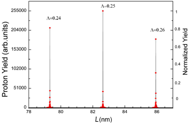
Figure 7 indicates that axial yield (flux) of the channeled protons in the transverse position plane, for the fixed value of the crystal tilt angle φ = 0.10 and different crystal thicknesses: L = 79.32, 83, and 85.93 nm, i.e., corresponding to points: Λ = 0.24, 0.25, and 0.26, presents a strongly damped function of nanocrystal thickness with a periodic behavior. Note that, maxima and minima presented in Figure 7 gradually become less prominent with increase of silicon nanocrystal thickness.
Calculated maximal axial flux intensities for super-focused proton beam in the transverse position plane. The fixed zero tilts parameters, φ = 0, are taken in different positions relative to nanocrystal channel <111> axis corresponding to points: Λ = 0.24, 0.25, and 0.26. The distance between the maxima of the proton yields induced by channeled proton confinement field is calculated via π2ħ2(n + 1/2)/(L2 m e), L = 100 nm, for n-discretized 2-d proton nanocrystal crystal potential.
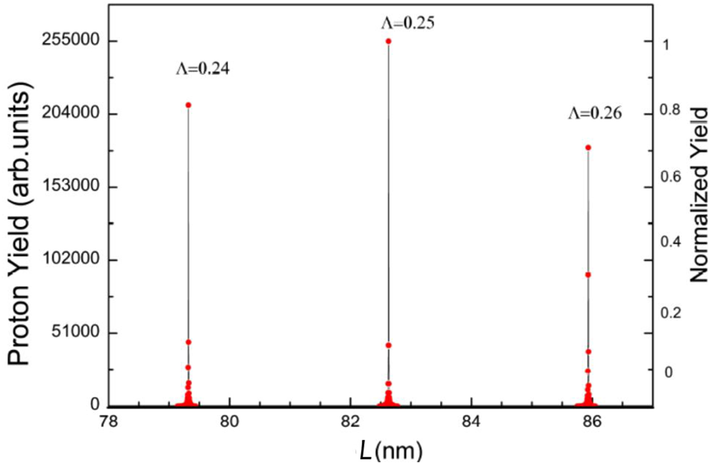
Further analysis inside the region: −a 0 ≤ L point at 83 nm ≤ a 0 shows that only FWHM of the first pronounced maxima coincide with the proton beam super-focusing point, while the second and third maxima appear as a result of passing the rainbow lines (Krause et al., Reference Krause, Barrett, Datz, Dittner, Jones, Gomez and Vane1994; Nye, Reference Nye1999) through the transverse position plane of the nanocrystal. From the point of view of longitudinal spatial resolution, the quantitative analysis shows that proton beam obtained with nanocrystal tilt φ = 0.10, for Λ = 0.24, 0.25, and 0.26, enters into the cylindrical region which corresponds to one-tenth of the Bohr radius 0.1a 0 = 0.0053 nm around the channel axis, i.e., this is the analyzed length of the super-focusing area. The obtained results further confirm the focusing of protons into the region whose dimension is much smaller than the average radius of a hydrogen atom in its ground state.
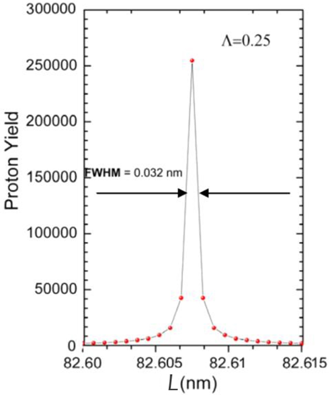
Figures 8 and 9 shows the FWHM and three-dimensional spatial projection of hyperchanneled proton beam flux distribution simulated in the transverse position plane, for zero degree nanocrystal tilt angle. It is important to note that only this flux peak represents singular proton yield, i.e., the flux of channeled protons has absolute maximum for φ = 0.
The proton axial yield projection in the transverse position plane at the super-focusing point (Λ = 0.25), for angle φ = 0, numerical simulation results obtained using the FLUX code.

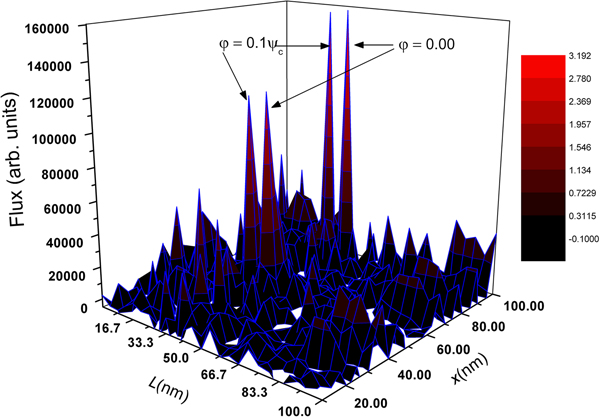
Comparison of the proton beam intensity profiles (different transverse cross-sections) for the tilt angle φ = 0.10ψc that corresponds to 10% of the critical angle for channeling, relative to super-focusing point, obtained for different longitudinal (L) and transversal (x) thickness of the nanocrystal, numerical simulation results obtained using the FLUX code.

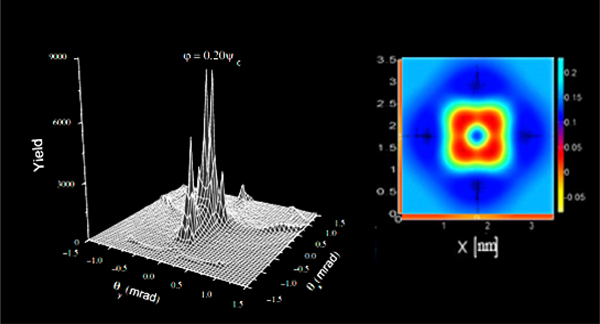
The subatomic scanning resolution (Breese et al., Reference Breese, Jamieson and King1996) obtained via different proton beam intensity profiles, illustrated by Figure 9, is calculated up to crystal tilt 0.10ψc corresponding to different longitudinal (L) and transversal (x) thicknesses. Total resolution is determined by the ratio of the inserted phosphorous atom diameter and the full-width of the proton beam. For this case, the calculated ratio is 20, which well corresponds with Slater (Reference Slater1964). In this case, the sensitivity of the spectroscopy is determined by the way the cross-section depends on the electron waive density. Sampling by angular (ϑ) parameter (Eq. (8)) up to 20% of the critical angle is enough to resolve electron DOS, showing the nodal structures in 〈111〉 silicon nanocrystal channel, as can be seen in Figure 10.
Right: two-dimensional intensity profile of the highest occupied atomic orbital representing electron DOS in 〈111〉 silicon nanocrystal channel obtained for the beam angle 0.20ψc. Left: 3d-surface slices in angular-exit nanocrystal plane obtained for the same angle, 0.20ψc.

CONCLUSIONS
We have demonstrated, theoretically and numerically, the ability of pulse-generated hyperchanneled protons to measure the three-dimensional structure of atomic orbitals. By using the coupled-channel calculation formalism we clarified an intimate connection between the electron DOS and the harmonic component of the proton-crystal interaction potential induced by the channeling relative to silicon nanocrystal <111> axis, and demonstrated the achievable coherent control obtained via super-focused proton beam in the silicon nanocrystal, aimed to produce a single nanolaser capable for scanning the interior of an atom within the region below the Bohr radius for all of considered values of the proton beam incident angles.
ACKNOWLEDGMENT
The Author is thankful to Dr. I. Anicin on fruitful discussions. This work is supported from Ministry of Science and Education under the MPNT project.