
I. INTRODUCTION
Fullerenes are probably the most interesting material having carbon atoms rolled up in spherical configuration. Reference Fowler and Manolopoulos1–Reference Winter and Kuzmany5 The multitudinous approaches have been developed to produce this alien material for the native applications. Reference Stephens, Cox, Lauher, Mihaly, Wiley, Allemand, Hirsch, Holczer, Li, Thompson and Wudl6–Reference Ruoff, Tse, Malhotra and Lorents8 The famous C60 Buckminsterfullerene was first introduced in 1985 Reference Kroto, Heath, O’Brien, Curl and Smalley9 and since then peculiar attempts are being explored to produce its family variants, especially the smaller fullerenes. The smaller fullerenes, usually called the nonclassical ones, are analogous to the number of carbon atoms present in the cage with at least 12 pentagons (as that in the smallest structure, C20). Reference Xu, Zhang, Zhao, Chen, Zhang and Sun10 None of these fullerenes follow the isolated pentagon rule (IPR), but convoy pentagon adjacency penalty rule (PAPR) Reference Kroto11–Reference Albertazzi, Domene, Fowler, Heine, Seifert, Van Alsenoy and Zerbetto13 to determine its stability. In this paper, we consider the first five smallest fullerenes, C20, C24, C26, C28, and C30 with Ih, D6d, D3h, D2, and D5h symmetry and zero, two, three, four, and five hexagons along with 12 pentagons in their cages respectively. These exceptional materials are contemplated in the two probe device junctions with fullerene molecule sandwiched between semi-infinite gold electrodes. The property of this standardized structure depends on the types of molecules and their characteristics. Reference Aradhya and Venkataraman14–Reference Aviram and Ratner16
The smallest member, C20 fullerene was first experimentally produced by H. Prinzbach et al. Reference Prinzbach, Weiler, Landenberger, Wahl, Wörth, Scott, Gelmont, Olevano and Issendorff17 and has been studied as a molecule Reference Sokolova, Lüchow and Anderson18,Reference Spagnolatti, Bernasconi and Benedek19 and as device mode within 1-D Reference An, Yang, Wang, Ma and Wang20 and 3-D gold electrodes. Reference An, Yang, Wang, Ma and Wang21 The next member, C24 fullerene had been scrutinized in molecular model Reference Jensen and Koch22,Reference An, Shao, Bulusu and Zenga23 and in 3-D gold electrodes Reference Zhao, Yang, Zhao, Wang and Ma24 for its orientation angle of 0–90° along with its transmission and current curves. In 2013, M. Kaur et al. Reference Kaur, Sawhney and Engles25 compared the pure C24 and its doped variants in device configurations using semiempirical extended Hückel theory. It was concluded that the pure C24 exhibits superconductive behavior as compared to other doped molecules. The various published works on C26 fullerene had utilized this molecule only for molecular mode Reference Kent, Towler, Needs and Rajagopal26–Reference An, Gan, Zhao and Li30 to search it lowest energy isomer with D3h symmetry. The relative energies, electronic structure, and growth mechanisms were carried out for C28 fullerene in Refs. Reference Martin31–Reference Mishra, Lin and Lee33 for its stable structures. In 2014, the electronic transport properties of pristine C28 fullerene and its doped variants were compared in two probe device configurations by plotting its transmission and current curves. Reference Pahuja and Srivastava34 The energy cut off and k-points were fixed at 400 Rydberg and 3 × 3 × 30 k-points, which themselves seem ambiguous. A study on the electronic and structural properties of C30 fullerene was done and was compared with C18N12 Reference Song, Parker, Schoendorff, Kus and Vaziri35 in molecular mode. A combined density functional study on carbon clusters, including C20, C24, C26, C28, and C30 was done by R.O. Jones in 1999 Reference Jones36 for structural and cohesive properties. Later in 2004, the electronic delocalization and electrical transport of smaller fullerenes namely, C20, C24, C28, C30, C32, and C60 are compared for their charging energies. Reference Zhang, Feng, Lee and Bai37
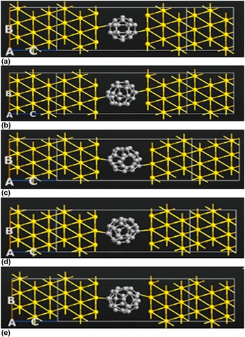
In our prior published work, we scrutinized the C20 fullerene stringed to gold electrodes for the full-fledged understanding of its electronic and electrical parameters. Reference Kaur, Sawhney and Engles38 Later, we investigated C20 fullerene sandwiched to different metallic electrodes for its charge and ballistic transport. Reference Kaur, Sawhney and Engles39 In this current work, we compare the electron transport behavior of C20, C24, C26, C28, and C30 devices formed by stringing these to gold electrodes (Fig. 1) and all the calculations for the comparison of the C20 device have been fetched from our earlier published work. Reference Kaur, Sawhney and Engles38
The nonclassical fullerenes (a) C20, (b) C24, (c) C26, (d) C28, and (e) C30 stringed to semi-infinite gold electrodes to form two probe junctions.

II. THEORY
A molecular junction device can be defined as a device formed when one or more molecules are implanted between a pair of electrodes having an equal magnitude of electrochemical potential. However, when a bias voltage is applied to molecular junctions, the electrochemical potential becomes the function of bias voltage and hence the electrons from one electrode are transferred within the bias window. Some electrons get transmitted while few are reflected Reference Guldi and Martín2 which subsequently results in nano-scale current at the nonequilibrium condition. To make two probe devices computable, we divide these into three subparts: left electrode, central region, and the right electrode. The left and right electrodes are formed of gold electrodes having (111) miller planes. The only criterion for selecting a particular length of the electrodes is to make sure that there are either no or negligible interactions with the second-nearest neighbor cell in the transport direction. In this context, we have calculated the electrode length to be 7 Å. The central scattering region encircles the nonclassical fullerene molecule and three surface layers of the electrodes with 1 × 1 × 100 k-point grid for the sampling in the transverse Brillouin plane. While modeling, we have selected the mechanically controllable break junctions (MCBJ) approach where the single physical contact between gold electrodes and molecule can be adjusted mechanically. The junction is formed by mechanically stretching the gold wire up to its breaking point. This pair of gold electrodes is exposed to the fullerene molecules, thus forming an organic molecular bridge.
The formalism used to obtain the results of the device is the popular density functional theory (DFT)–nonequilibrium green’s function (NEGF) method by their implementation on Atomistic Tool Kit-Virtual Nano Lab (ATK-VNL) software. Reference Stokbro40,41 We used high-level double zeta polarization (DZP) basis set for all atomic species in conjunction with exchange-correlation potential, Perdew–Burke–Ernzerhof-Generalized Gradient Approximation (PBE-GGA) of DFT without making any comprise to precision. Reference Strange, Kristensen, Thygesen and Jacobsen42 The atomic cores are elaborated by norm-conserving Troullier–Martins pseudo-potentials. Reference Troullier and Martins43 The electrostatic potentials are determined on a real-space grid with mesh cut-off energy of 150 Rydberg a.u.
The DFT-NEGF method has become the standard approach for modeling nonequilibrium quantum transport in atomistic nanostructures. This DFT-NEGF approach is explained in following steps: (i) the density matrix (for equilibrium and nonequilibrium states) is computed from the energy integral of Green’s function, (ii) the density of states (DOS) and electron density for devices are obtained, (iii) the transmission function is calculated. After performing these tasks, it becomes imperative to calculate the electrical characteristics of the molecular bridge. The current at nanometer scale is calculated from the transmission coefficient using the relation,
 $$I = {e \over h}\sum\limits_\sigma {\int {{T_\sigma }\left( E \right)\left[ {f\left( {{{E - E_{\rm{F}}^{\rm{L}} + e{V_{\rm{R}}}} \over {{k_{\rm{b}}}{T_{\rm{R}}}}}} \right) - f\left( {{{E - E_{\rm{F}}^{\rm{L}} + e{V_{\rm{L}}}} \over {{k_{\rm{b}}}{T_{\rm{L}}}}}} \right)} \right]} } {\rm{d}}E\quad,$$
where f is the Fermi function,
 $E_{\rm{F}}^{\rm{L}}$
is the Fermi energy, and T
L and T
R are the electron temperatures of the left and right electrodes, respectively. In the above equation, T
σ(E) is the transmission coefficient for spin σ. The differential conductance is calculated from the transmission function by performing numerical differentiation
 $${\rm{d}}G = {{{\rm{d}}I} \mathord{\left/ {\vphantom {{{\rm{d}}I} {{\rm{d}}V}}} \right. \kern-\nulldelimiterspace} {{\rm{d}}V}} = {{I\left( {{V_{\rm{R}}},{T_{\rm{L}}},{T_{\rm{R}}}} \right) - I\left( {{V_{\rm{L}}},{T_{\rm{L}}},{T_{\rm{R}}}} \right)} \over {{V_{\rm{R}}} - {V_{\rm{L}}}}}\quad.$$
The simulation procedure is repeated for all the four devices formed at variable bias voltages of −2 V to +2 V with a step size of ±0.2 V.
III. RESULTS AND DISCUSSIONS
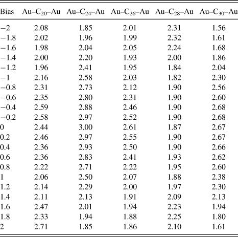
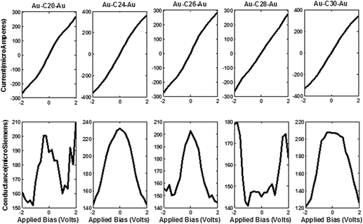
The performed computations result in two vital electrical parameters: current and conductance calculated from Eqs. (1) and (2) and are plotted in Fig. 2. The quantum of conductance (G 0) Reference van Wees, van Houten, Beenakker, Williamson, Kouwenhoven, van der Marel and Foxon44 (Table I) as given by Landauer formula, 2e 2/h is independent of the material properties.
The I–V and G–V curve for Au–C20–Au, Reference Kaur, Sawhney and Engles38 Au–C24–Au, Au–C26–Au, Au–C28–Au, and Au–C30–Au.

Quantum of conductance (G 0) for Au–C20–Au, Reference Kaur, Sawhney and Engles38 Au–C24–Au, Au–C26–Au, Au–C28–Au, and Au–C30–Au.

The physical significance of electrical current is to impart the drift on charges that describe local currents in the molecular device. The sum of the local currents through any surface perpendicular to the z-direction is identical that demonstrates the charge conservation in molecular devices. Reference Solomon, Herrmann, Hansen, Mujica and Ratner45 Hence, the current curves are linear in nature. The highest magnitude of the current is observed for Au–C24–Au along with its asymmetric nature for both the bias polarities. This asymmetry in the current curve is measured by the rectification ratio (+I/−I) that decreases for lower bias up to ±1 V and increases afterward. The current curves for Au–C26–Au and Au–C28–Au device are similar in its linearity nature with higher magnitude for positive voltages giving the rectification ratio greater than unity. However, the current characteristics for Au–C30–Au are similar to Au–C20–Au Reference Kaur, Sawhney and Engles38 with its asymmetry being highest at ±1 V and decreasing otherwise.
Another observable electrical quantity is the differential conductance, which determines the way molecules remain coupled to the electrodes. The differential conductance for Au–C20–Au, Reference Kaur, Sawhney and Engles38 Au–C24–Au, Au–C26–Au, and Au–C30–Au indicate the lifting of Coulomb blockade at the lower bias voltages. Also, these devices exhibit huge disparity in conductance magnitude for both lower and higher biases. The observed conductance for the Au–C24–Au is 3G 0 and 1.85G 0 for 0 V and ±2 V, respectively (Table I). However, in the Au–C28–Au device, there is the least difference normally in conductance values. Moreover, there is absence of Kondo peaks observable at zero bias. Rather a slight dip is visible with 1.87G 0 that indicates the conductance gap between ±1 V. Hence after elucidating current and conductance characteristics, we observe the order of conducting nature as Au–C24–Au followed by Au–C30–Au, Au–C26–Au, Au–C20–Au, and Au–C28–Au respectively.
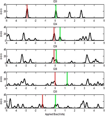
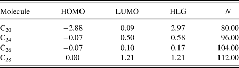
Since this current is the number of available states in the molecule filled per second and the electrons in electrodes are filled up up-to its chemical potential, the electrons cannot jump into higher energy states in the molecule. To check the validity of the electrical parameters discussed above, we analyze the fullerene molecules for both molecular and device mode. The investigative details have been explained in three sections: for isolated molecule, for the device at zero bias and for the device at variable bias voltages. The calculated results are compared with the results predicted for pure C20 fullerene device. Reference Kaur, Sawhney and Engles38 First, the DOS and the molecular orbitals for isolated fullerene molecules are calculated using the PBE-GGA parameterization as presented in Fig. 3 and Table II.
DOS of C20, Reference Kaur, Sawhney and Engles38 C24, C26, C28, and C30 fullerenes in their molecular mode. The vertical red and green lines represent HOMO and LUMO levels. The values for the C20 molecule are interpreted from Ref.Reference Kaur, Sawhney and Engles38.

Various parameters of an isolated fullerene molecule.

These parameters determine the crucial effects which influence the quantum transport in the junction devices. As we all know that the DOS represents the number of accessible states for conduction at energy levels and their magnitude is indicated by the discrete peaks. To calculate the DOS, we assume the isolated molecule as ‘particle in a box’ and approximate it by a homogeneous box with the confinement of electrons within. The number of discrete peaks increases as we increase the number of carbon atoms in the fullerene cage. There are peaks present at the energy levels of two immediate molecular orbitals: highest occupied molecular orbital (HOMO) and lowest unoccupied molecular orbital (LUMO). The isolated C20 and C30 molecules are conducting through LUMO level but the magnitude of its DOS peak is slightly smaller than HOMO level-DOS peak. For the rest of three molecules—C24, C26, and C28, the transport is through HOMO level with Fermi level being exactly on the HOMO level for C30 molecule. Moreover, the HOMO–LUMO gap (HLG) is lowest for C26 and C24 molecules with magnitudes of 0.17 and 0.58 eV (quite near to that calculated in Ref. Reference Zhao, Yang, Zhao, Wang and Ma24). The HLG is highest for C20 with 2.97 eV with this being the most stable isomer in smaller fullerene family. Reference Kaur, Sawhney and Engles38 The electron density (N) is also arranged in Table II and is expressed by N = 4 × n, where n is the number of carbon atoms in fullerene molecule.
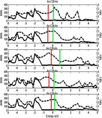
As the methods for obtaining the density matrix in equilibrium and nonequilibrium conditions differ, we have contemplated the devices both at zero as well as varied bias voltages. The aim here is to verify the physical process taking place in the junction devices on the application of zero bias voltages. When an isolated molecule is placed in between the pair of semi-infinite electrodes, its discrete DOS peaks infuses with the continuum states of gold electrodes and results in DOS of the central scattering region broadened by Lorentzian type as shown in Fig. 4. Most of the high magnitude peaks are visible before the HOMO level, that indicates the frozen states which are already filled up within the central region and leaving an only small portion of density actually participating in conduction process.
DOS and T(E) are marked in solid and dashed lines respectively. The vertical red and green lines represent HOMO and LUMO levels. The values for the Au–C20–Au device are interpreted from Ref. Reference Kaur, Sawhney and Engles38.

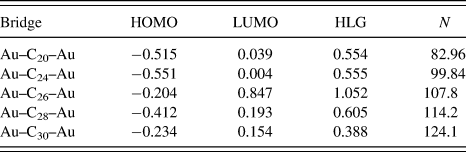
The amplitude of the transmitted wave that passes through the quantum barrier formed at a point when an isolated molecule is placed in between metal electrodes, is given by transmission coefficient, T(E) (Fig. 4). It represents the extent of transfer of charge within the device formed. The broadened and high magnitude of peaks indicates the higher capability of charge transfer as this is the result of strong delocalization of molecular states with those of electrodes over an interface. The transmission spectrum for Au–C24–Au device is similar to that plotted in Ref. Reference Zhao, Yang, Zhao, Wang and Ma24. The comparison of DOS and T(E) anticipate the molecular orbitals as arranged in Table III. The energy levels of conducting orbital (HOMO or LUMO) represents the higher magnitude and broadened peaks in DOS and T(E) for four devices except in Au–C28–Au device. In this device, the magnitude of T(E) is lower and is least broadened at LUMO level that results in absence of Kondo peak at zero bias in its G–V curve (Fig. 2 and Table I). One more interesting fact is visible in the transmission spectra of C24 and C30 devices that the T(E) is highest for both HOMO and LUMO levels, which indicates the higher equilibrium conductance at zero and varied bias voltages (Tables I and III). Thus the differential conductance curves obtained from T(E) are directly proportional to each other.
Various parameters in molecular bridges formed.

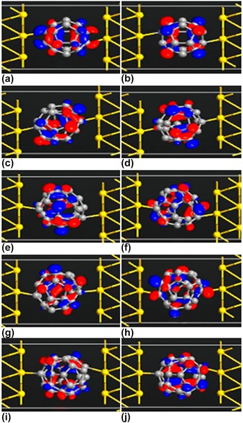
Moreover, the conduction through HOMO in the isolated molecule has changed to LUMO in C24 and a C28 device that indicates the increase in coupling when the molecules are placed within gold electrodes. However, the conducting orbital i.e., HOMO, LUMO, and LUMO remains same in C26, C20, and C30 devices respectively. The molecular projected self-consistent Hamiltonian (MPSH) states at HOMO and LUMO for five devices are presented in Fig. 5. The conducting levels demonstrate the higher extent of delocalization of molecule with gold electrodes.
MPSH states (left column: HOMO and right column: LUMO) for Au–C20–Au (a) and (b), Reference Kaur, Sawhney and Engles38 Au–C24–Au (c) and (d), Au–C26–Au (e) and (f), Au–C28–Au (g) and (h), and Au–C30–Au (i) and (j). The red and blue color of the states represents different orbital phases.

When an isolated molecule forms a two-junction device, there is often a decrease in HLG as depicted in Table III. However, the HLG of Au–C26–Au device has increased from 0.17 eV to 1.052 eV and is conducting through HOMO. The HLG within Au–C24–Au and Au–C20–Au devices are approximately same at zero bias yet there are huge differences in their I–V and G–V curves. This might be an indication of some different phenomena occurring in transport process within the junctions. The N has increased for a stringed molecule from the isolated one as this augmentation is contributed by electron density of the connected interfaces along with delocalized electrons from the fullerene molecule.
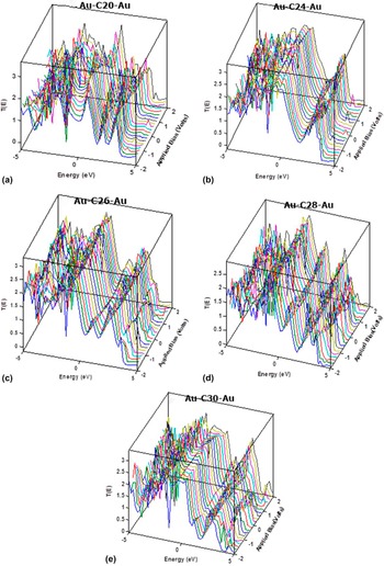
The scrutiny at zero bias reveals the slight picture of stringed molecules in device formation. For greater insights, we contemplate the transmission probability, along with their molecular orbitals and energy levels at a variable bias of −2 V to +2 V. First, the transmission probabilities at different bias for different devices are plotted with respect to energy and voltages in Fig. 6.
Transmission probability for (a) Au–C20–Au, Reference Kaur, Sawhney and Engles38 (b) Au–C24–Au, (c) Au–C26–Au, (d) Au–C28–Au, and (e) Au–C30–Au at bias voltages for energy levels of −5 eV to +5 eV. The Fermi energy is considered as 0 eV. The values for T(E) for C20 is interpreted from Ref. Reference Kaur, Sawhney and Engles38.

As discussed earlier, the T(E) is accountable for the flow of charge in nonequilibrium condition and subject to electrons responsible for conduction at different orbitals. The width and height of peaks indicate the measure of the performance of molecule under the effect of electrodes. In Fig. 6, the shifting of transmission peaks within the bias window illustrates the change of molecular orbitals during the ballistic transport. This phenomenon happens in Au–C20–Au and Au–C26–Au devices with conduction through LUMO Reference Kaur, Sawhney and Engles38 and HOMO orbitals respectively. Another effect is visible in Au–C24–Au and Au–C30–Au devices that they have quite broad and smooth transmission that indicates strong coupling behavior of fullerene molecules with gold electrodes and thus lead to large currents at low bias. However, in the case of Au–C28–Au, there are prominent dips in the transmission at Fermi level with conducting LUMO lying on the tail of its transmission peak. Thus, this is indeed reason that led to lowest current and conductance values as shown in Fig. 1.
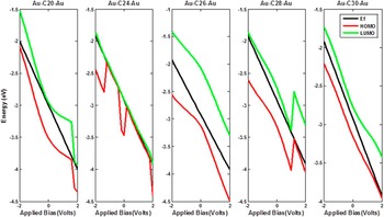
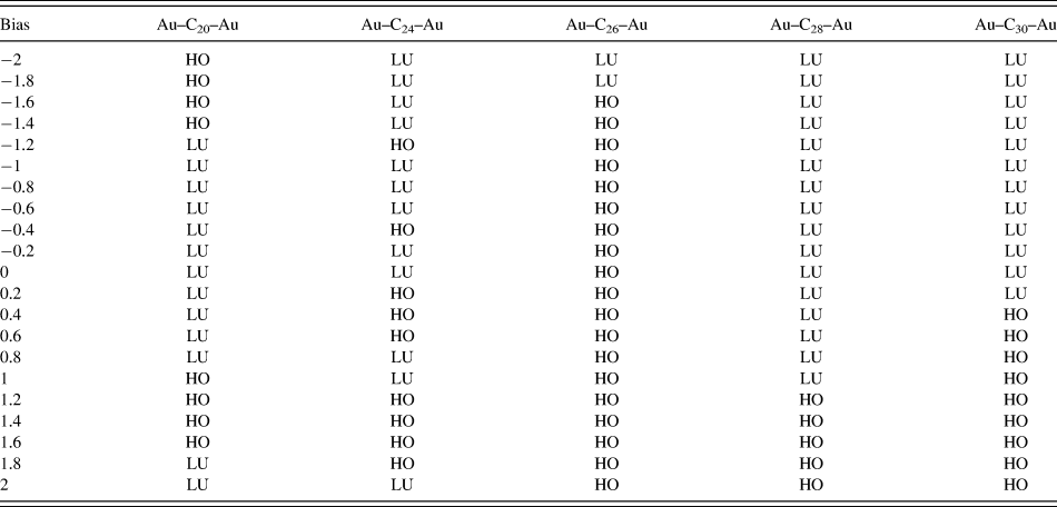
The transmission spectra reveal the position of HOMO and LUMO levels and are plotted with its Fermi level in Fig. 7 as their energy level diagram. In general, transmission peaks closer to the Fermi level dominate the conduction in different bias region as the fullerene molecule is equispaced between the symmetric gold electrodes, i.e., its voltage division factor, ƞ is 0.5. The calculated active molecular orbital accountable for conduction process is arranged in Table IV. The energy level diagram illustrates the change in active molecular orbitals with respect to its Fermi level. For a fullerene device to work in an ideal conducting manner, it works in HOMO–LUMO–HOMO specifications at higher-lower-higher bias voltages. We elucidate that such an ideal behavior is present in an Au–C20–Au device with its breakdown at a higher voltage of +1.8 V. Reference Kaur, Sawhney and Engles38
Energy level diagram for Au–C20–Au, Reference Kaur, Sawhney and Engles38 Au–C24–Au, Au–C26–Au, Au–C28–Au, and Au–C30–Au.

Active molecular orbital levels at different bias voltages.

However, in the case of Au–C24–Au, the device has a number of variations in energy level diagram with two breakdowns. The first breakdown happens at low bias voltages of −0.6 V and +0.8 V, while its second breakdown occurs at −1.4 V and +2 V where the active orbital is LUMO. The ability of Au–C24–Au device to adapt to the change in molecular orbitals has lead to huge current and conductance for this device. Moreover, this unambiguously suggests that the first breakdown condition in the molecular junction is sometimes essential for a nano-device to work in much similar way to the Zener breakdown visible in heavily doped p–n junctions. After the second breakdown condition, the device loses its ability to conduct electrons and finally ruptures indicating the initiation of avalanche breakdown. This indicates that the electrons from left electrode drift with full force toward the right electrode assisted with the progressive role of a fullerene molecule. This phenomenon results in the ballistic transport in C20 and C24 device junctions.
In Au–C26–Au device, the conduction at zero bias and at varied bias voltages (−1.6 V to +2 V) is through HOMO levels and is characterized as ‘hole transport’. This is quite contrasting to the other nonclassical fullerene devices Reference Kaur, Sawhney and Engles39 that demonstrate strong coupling with the gold electrodes. In Au–C28–Au device, there is a visible change in active molecular orbital from LUMO to HOMO at +1.2 V. Similarly in Au–C30–Au device, the active molecular orbital has changed from LUMO to HOMO at comparatively low bias voltage of +0.4 V that predicts the presence of high asymmetry in conjunction of C30 molecule with its electrodes.
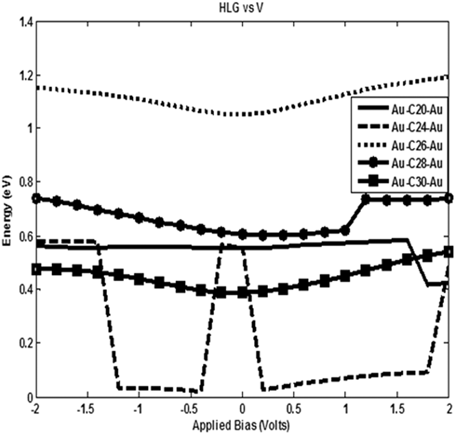
The two devices Au–C28–Au and Au–C30–Au, perform conduction through LUMO level at higher negative voltages but still do not undergo any kind of breakdown. This indicates the weak coupling of C28 and C30 molecules to its electrodes. Alongside, we have calculated HLG from the energy level diagram and are plotted in Fig. 8 for the five devices scrutinized.
HLG for Au–C20–Au, Reference Kaur, Sawhney and Engles38 Au–C24–Au, Au–C26–Au, Au–C28–Au and Au–C30–Au.

The HLG for all five devices are compared and observed to be highest (>1 eV) for Au–C26–Au as the active orbital in the conduction process is HOMO. For rest of four devices, the HLG is found less than 1 eV and least for the C24 device. For zero bias, the HLG of the C24 device is similar to that of C20 device as indicated above in Table III but the real picture is actually depicted at variable bias voltages. In Au–C20–Au device, HLG reduces at its first breakdown point of +1.8 V, where it conducts through LUMO. In Au–C24–Au device, HLG is highest at −0.2 and 0 V, decreases afterward for intermediate range of voltages and then increases at its second breakdown voltages, −1.4 V and +2 V. In Au–C28–Au, the HLG has increased at +1.2 V indicating the change in its active orbital. The HLG for Au–C30–Au device has increasing unexpectedly HLG with an increase of bias voltages without rising explicitly but does not reveal the actual picture according to its molecular orbitals. Thus, the contemplation of transmission probability, molecular orbitals, and energy levels at a variable bias of −2 V to +2 V definitely helps in understanding various phenomena enduring beneath. But we reconcile and supplement this insight by analyzing the N and the charge transfer occurring at zero and varied bias voltages.
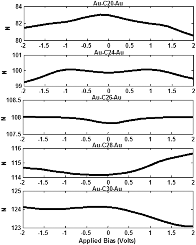
The N is deliberated from the density matrix and is plotted in Fig. 9. The N defines the occupied states of the fullerene molecule in device system and is never an absolute quantity. The electron density decreases with increase in bias voltages for both polarities for Au–C20–Au. Reference Kaur, Sawhney and Engles38 Though a similar effect is visible for Au–C30–Au but the fall is not as prominent for negative voltages. However, N has increased with increase in bias voltages for Au–C26–Au and Au–C28–Au devices. In Au–C24–Au device, N is low for zero bias as well as for higher bias, while has increased for intermediate voltages, indicating its behavior to be inversely proportional to its HLG. One more intersecting conclusion that has delineated from N is about the asymmetry in conjunction of fullerene molecules with respect to their gold electrodes.
N for fullerene molecules in Au–C20–Au, Reference Kaur, Sawhney and Engles38 Au–C24–Au, Au–C26–Au, Au–C28–Au, and Au–C30–Au.

The C20 and C30 are strongly coupled to left gold electrode Reference Kaur, Sawhney and Engles38 as we apply bias voltages to the left electrode and keeping the right electrode at the ground position. This is the result of higher absorption of charges in left electrode when we apply a positive bias to the left electrode. The situation is opposite in the case of C24 and C28 devices where the molecules strongly hinge with the right gold electrode. However, in the case of the C26 device, the molecule is symmetrically aligned with both the gold electrode and is conducting through HOMO level for entire bias range. Hence, there is an observable accumulation of charges at the molecule-electrode interface that leads to asymmetry in the coupling.
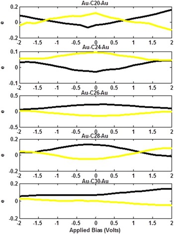
The charge transfer presented in Fig. 10 is the summation of the electronic charge transfer in the molecule (or electrodes) and charge injected or extracted at interfaces. The electron density and participating density in the ballistic transport are different in magnitude as only those charges perform in the conduction process that lies near the Fermi surface or so-called imaginary surface formed within the central region. Reference Kaur, Sawhney and Engles38
Charge transfer for Au–C20–Au, Reference Kaur, Sawhney and Engles38 Au–C24–Au, Au–C26–Au, Au–C28–Au, and Au–C30–Au. The black and yellow lines represent the charge transfer in fullerene molecules and gold electrodes respectively.

In the case of Au–C20–Au and Au–C24–Au, the fullerenes exhibit their strong metallic character with negative charge transfer in lower bias range. Reference Kaur, Sawhney and Engles38 This indicates that C20 and C24 are accounting their attributes without being dominated by the electrodes. However, this domination is minimal at higher bias voltages for the C24 device that concludes it to be very conductive in nature when stringed to gold electrodes, rather better than even C20 device. We can say that gold electrodes are not exhibiting their metallic character when stringed to C24 fullerene, but still, this device is working as a superconductor as indicated in Ref. Reference Kaur, Sawhney and Engles25. In Au–C26–Au and Au–C28–Au device, ones with increasing value of N at an increase of bias voltages, have the most imposing role of electrodes at lower bias. This reduces with increases in bias voltages despite the fact that the former device is conducting through HOMO while later through LUMO. However, in the case of Au–C30–Au device, the asymmetry in molecule-electrode coupling is observed highest with C30 demonstrating its metallic character only for positive voltages. This device exhibits contrasting behavior for negative bias voltages as it is conducting through HOMO and thus is weakly coupled to right electrodes. Such attributes were not visible in the contemplation of current, conductance, and its orbital gap. The deliberation of active molecular orbitals, N and charge transfer are concluded as highly important for the physical understanding and reliability of the device constructed. Hence, we supplemented the investigation of electrical parameters with sufficient and necessary abstraction of the electronic and physical parameters.
IV. SUMMARY
In the present work, we utilize the DFT-NEGF formalism to compare the nonclassical fullerene devices formed by two probe MCBJ devices. The molecular junctions consisting of various variants of fullerenes molecules (C20, C24, C26, C28, and C30) are stringed to the gold electrodes having miller indices of 1:1:1. The smallest fullerene device Au–C20–Au, Reference Kaur, Sawhney and Engles38 has been compared with the other four devices that we developed for further elucidation. First, the two vital electrical parameters, current and conductance are scrutinized. This section concludes about the conducting nature of devices as Au–C24–Au > Au–C30–Au > Au–C26–Au > Au–C20–Au > Au–C28–Au. Then, we contemplate the electronic and physical aspects of the isolated fullerene molecule, fullerene devices at zero, and variable bias voltages. The various parameters namely, DOS, T(E), molecular orbitals, electron density, and charge transfer are investigated as the proof for the electrical measurements. The results conclude that the C24 fullerene molecule exhibits metallic performance with gold electrodes. This device reveals the superconductive behavior of C24 fullerene with an ability to easily adapt under the effect of potential bias by modulating its active molecular orbitals. Also, this device is comparatively similar to Au–C20–Au device, but possessing quite higher currents. In Au–C26–Au device, the conduction at zero bias as well as at varied bias is through HOMO level and is thus characterized as ‘hole transport’. The two devices, Au–C28–Au and Au–C30–Au perform this conduction through LUMO level at higher negative voltages but still do not undergo any kind of breakdown that indicates the weak coupling of C28 and C30 molecules to gold electrodes. We conclude that the deliberation of active molecular orbitals, N and charge transfer are highly important for the physical understanding and reliability of the devices to be constructed.