
I. INTRODUCTION
The synthesis of complex oxides with multiple transition metals has attracted much attention in the past decades as these materials could exhibit emergent properties. Recent advances in controlled growth of thin films have provided unique opportunities to grow novel complex oxides, which are inaccessible in bulk process. Pulsed laser deposition (PLD) is a relatively simple and very versatile technique for thin film growth. Reference Narayan, Biunno, Singh, Holland and Auciello1 Different architectures including heterostructures, Reference Allibe, Infante, Fusil, Bouzehouane, Jacquet, Deranlot, Bibes and Barthelemy2–Reference Su, Cho, Bi, Chen and Wang4 superlattices, Reference Li, You, Yang, Tan, Ren, Chen, Pan, Wang, Wang, Bosman, Zhu and Dong5–Reference Yadav, Nelson, Hsu, Hong, Clarkson, Schlepuetz, Damodaran, Shafer, Arenholz, Dedon, Chen, Vishwanath, Minor, Chen, Scott, Martin and Ramesh7 and vertical heteroepitaxial nanocomposites, Reference Chen, Bi, Tsai, Lee, Su, Zhang, Jia, MacManus-Driscoll and Wang8–Reference Zhang, Chen, Jian, Zhu, Chen, Lu, Jia, MacManus-Driscoll, Zhang and Wang10 have been reported. Recent efforts on vertical heteroepitaxial nanocomposites have been focused on the development of multifunctionalities by combining two immiscible phases. Reference Aimon, Choi, Sun, Kim and Ross11–Reference Chen, Hu, Lu, Yang, Zhang, Li, Ahmed, Enriquez, Weigand, Su, Wang, Zhu, MacManus-Driscoll, Chen, Yarotski and Jia17 Immiscibility is one of the key factors for nanocomposite formation. Reference MacManus-Driscoll18 On the other hand, the co-growth of two miscible or partially miscible phases can lead to unexpected phases. Reference Chen, Zhou, Bi, Zhu, Luo, Bayraktaroglu, Phillips, Choi, MacManus-Driscoll, Pennycook, Narayan, Jia, Zhang and Wang19–Reference Li, Zhang, Khatkhatay, Jian, Fan, Su, Zhu, Chen, Lu, Zhang and Wang21 A representative system is ferroelectric BiFeO3 (BFO) in combination with ferromagnetic BiMnO3 (BMO) where double perovskites can be produced to achieve ferromagnetism and multiferroicity. Reference Choi, Patnaik, Weal, Sahonta, Wang, Bi, Xiong, Blamire, Jia and MacManus-Driscoll22–Reference Zhao, Kimura, Cheng, Wang and Nishida26 For example, Chio et al. reported room temperature multiferroic properties in strained BiFe0.5Mn0.5O3 thin films, Reference Choi, Fix, Kursumovic, Kinane, Arena, Sahonta, Bi, Xiong, Yan, Lee, Wang, Langridge, Kim, Borisevich, MacLaren, Ramasse, Blamire, Jia and MacManus-Driscoll27 and increased ferromagnetic Curie temperature in BFO/BMO superlattices. Reference Choi, Kleibeuker, Fix, Xiong, Kinane, Arena, Langridge, Chen, Bi, Lee, Wang, Jia, Blamire and MacManus-Driscoll28 Similarly, other materials with double perovskite structure such as Bi2NiMnO6 and Bi2FeCrO6 can be synthesized using the same scheme. Reference Azuma, Takata, Saito, Ishiwata, Shimakawa and Takano29–Reference Li, AlOtaibi, Huang, Mi, Serpone, Nechache and Rosei32
The microstructure (and thus the functionality) of a given material grown by PLD is influenced by many factors including substrate, gas pressure, temperature, laser frequency, and laser energy density. Substrate plays a critical role in epitaxial growth of thin film as the lattice mismatch between the film and the substrate determines the critical thickness. More importantly, substrate can be used to stabilize the phase if multiple phases co-exist for a given chemical composition. For example, LaAlO3 substrate was used to stabilize the anatase TiO2 phase while r- and m-sapphire substrates were selected for the growth of rutile TiO2 phase. Reference Lotnyk, Senz and Hesse33,Reference Park, Huang, Li and Jia34 VO2 (B) phase was found prone to grown on SrTiO3 substrate, whereas, VO2 (M) phase often found grown on c-sapphire by domain matching epitaxy. Reference Chen, Bi, Zhang, Jian, Jia and Wang35–Reference Gupta, Aggarwal, Gupta, Dutta, Narayan and Narayan38 Oxygen pressure during film growth is usually associated to the oxygen content in the metal oxide films. Reference Chen, Long, Li, Li, Yang and Lu39 Another important but often ignored effect induced by oxygen pressure is cation stoichiometry, Reference Chen, Khatkhatay, Zhang, Jacob, Jiao and Wang3,Reference Li, You, Yang, Tan, Ren, Chen, Pan, Wang, Wang, Bosman, Zhu and Dong5,Reference Golalikhani, Lei, Chen, Spanier, Ghassemi, Johnson, Taheri and Xi40–Reference You, Chua, Yao, Chen and Wang42 which is one of the key factors determining functional properties. Reference Warusawithana, Richter, Mundy, Roy, Ludwig, Paetel, Heeg, Pawlicki, Kourkoutis, Zheng, Lee, Mulcahy, Zander, Zhu, Schubert, Eckstein, Muller, Hellberg, Mannhart and Schlom43 In the case of growth temperature, it not only influences the film crystallinity and feature size, but also affects the phase structure. Reference Long, Yang, Chen, Li and Lu44 Regarding materials with high volatility such as bismuth, vanadium, and lithium, lower growth temperature below 700 °C is usually used. Reference Srivastava, Rotella, Saha, Pal, Kalon, Mathew, Motapothula, Dykas, Yang, Okunishi, Sarma and Venkatesan45–Reference Lu, Howard, Chen, Zhu, Li, Wu, Dowden, Xu, Zhao and Jia47 Laser repetition rate is found to alter the material structure. For example, it was reported that 5 Hz repetition rate results in VO2 (A) phase while 2 Hz results in VO2 (B) phase. Reference Srivastava, Rotella, Saha, Pal, Kalon, Mathew, Motapothula, Dykas, Yang, Okunishi, Sarma and Venkatesan45 In vertical nanocomposites, laser repetition rate can affect the feature size. Reference Chen, Bi, Jia, MacManus-Driscoll and Wang48 The laser energy density of the excimer lasers for the growth of metal oxide films typically ranges from 1 to 3 J/cm2. Laser energy density is often found to affect cation stoichiometry. Reference Golalikhani, Lei, Chen, Spanier, Ghassemi, Johnson, Taheri and Xi40,Reference Liu, Lei and Xi41,Reference Kan and Shimakawa49,Reference Kobayashi, Tokuda, Ohnishi, Mizoguchi, Shibata, Sato, Ikuhara and Yamamoto50 Hence, it is critical to maintain a uniform and stable laser energy density to reproducibly grow high quality films. Reference Dowden, Bi and Jia51
Bismuth compounds have different structures and are sensitive to growth conditions and substrate. Reference You, Chua, Yao, Chen and Wang42,Reference Bea, Bibes, Barthelemy, Bouzehouane, Jacquet, Khodan, Contour, Fusil, Wyczisk, Forget, Lebeugle, Colson and Viret46 Hence, studying the growth window for new phases in thin film form is critical. Alternatively, it is equally important to develop new and versatile strategies to broaden the growth window for desired thin film materials. In this work, we explored the growth of different phases of materials by using BiFeO3:BiMnO3 and BiFeO3:BiCrO3 composite systems. By varying the substrate, deposition temperature, laser repetition rate, and oxygen pressure, we have found the growth of several new phases which have not been reported in the literature. More importantly, we found that the CeO2 buffer layer, serving as a universal template, is capable of broadening the thin film growth window for new phases.
II. EXPERIMENTAL
PLD was used to grow epitaxial films on STO (001) and LAO (001) substrates. Composite targets, with a 1:1 molar ratio of Bi1.05FeO3 and Bi1.05MnO3, were obtained by conventional ceramic sintering process. The substrate temperature ranged from 650 to 725 °C and oxygen pressure of 15–200 mTorr were maintained during depositions. After deposition, films were in situ annealed for 1 h at 400 °C in an oxygen pressure of 300 Torr before cooling down to room temperature at 5 °C/min. Films with thickness from 10 nm to 300 nm were deposited. A set of thin films were deposited by systematically varying the deposition temperature, laser repetition frequency, deposition duration, oxygen pressure, and different buffer layers. Buffer layer CeO2 with a thickness of 25 nm was deposited at 700 °C between the film and the substrate. The microstructure was examined by X-ray diffraction (XRD; Bruker D8 powder X-ray diffractometer, Bruker Corporation, Karlsruhe, Germany; and PANalytical MRD PRO X-ray diffractometer, PANalytical, Almelo, The Netherlands) and transmission electron microscopy (TEM; JEOL JEM-2010, JEOL Ltd., Tokyo, Japan; and FEI Tecnai G2 F20, FEI Company, Hillsboro, Oregon). The high-angle annular dark-field scanning transmission electron microscopy (HAADF-STEM) images were taken by using a VG Microscopes HB603U STEM equipped with Nion aberration corrector operating at 300 kV at Oak Ridge National Laboratory (Oak Ridge, Tennessee).
III. RESULTS AND DISCUSSIONS
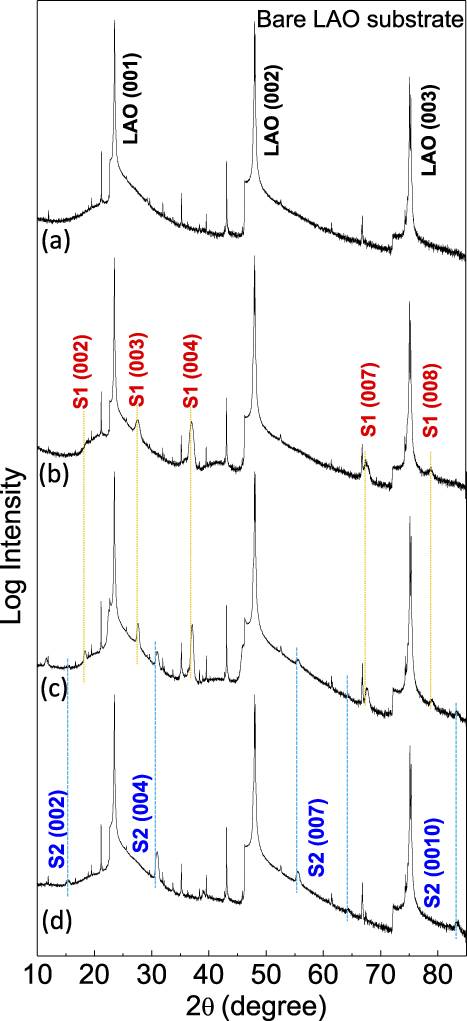
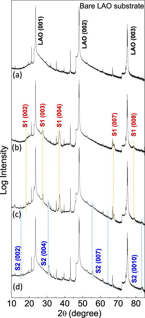
Figure 1 shows the effect of growth temperature and laser frequency on the films deposited using a BFO:BMO composite target. It can be seen that the phase of films is very sensitive to the growth parameters and the growth window for pure phase is narrow. Figure 1(a) shows a typical XRD θ–2θ scan of a bare LAO substrate from a powder X-ray diffractometer. Figure 1(b) shows the XRD of the film grown at 700 °C and 2 Hz. It can be seen that a single set of diffraction peaks (2θ = 18.28°, 27.57°, 36.96°, …), can be observed, indicating the growth of a single phase material. Reference Chen, Zhou, Bi, Zhu, Luo, Bayraktaroglu, Phillips, Choi, MacManus-Driscoll, Pennycook, Narayan, Jia, Zhang and Wang19 This phase is defined as S1 phase. The out-of-plane d-spacing of S1 phase is determined to be 4.85 Å. Increasing the laser repetition rate above 4 Hz and tuning the growth temperature either below 670 °C or above 700 °C, as shown in Fig. 1(c), result in mixed phases. Interestingly, when keeping the growth temperature at 725 °C and laser repetition rate at 1 Hz, the film shows a single set of diffraction peaks (2θ = 15.42°, 30.96°, 39.03°, …), indicating the growth of another pure phase (labeled as S2 phase). The out-of-plane d-spacing of S2 phase is determined to be 5.74 Å. The cation ratio for S1 phase is Bi:Fe:Mn = 3:2:2. We expect there are less Bi in S2 phase as it was grown at higher growth temperature and lower laser repetition rate. Thus, the thin film growth in BFO:BMO system is sensitive to the growth condition. The sensitivity of the growth likely stems from the volatilization of the bismuth at different growth conditions.
The XRD patterns of (a) bare LAO substrate, (b) film deposited at 700 °C, 2 Hz, (c) film grown at 700 °C, 4 Hz, (d) film grown at 725 °C and 1 Hz.
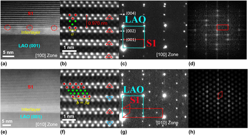
To study the microstructure of these materials, high resolution STEM has been used. Figure 2(a) shows a typical cross-sectional HAADF-STEM image for S1 phase grown on LAO (001) substrate. Interestingly, a highly strained interlayer is formed on top of LAO substrate before the growth of S1 phase. This interlayer is fully strained on LAO substrate with c/a = 1.15 and the formation of misfit dislocations are clearly seen between the interlayer and S1 phase. Figure 2(b) shows a HR-STEM image of S1 phase. Both Bi2O2 slab with brighter contrast and Fe–Mn–O slab with darker contrast show zig-zag arrangements. The spacing between the neighboring Bi2O2 layer is 9.70 Å, which is twice of the d-spacing corresponding to the peak at 2θ = 18.28°. The Bi atoms in Bi2O2 layer show the same atomic arrangement at the same column, as shown by red triangles in Fig. 2(b). The alternative stacking of Bi2O2 and Fe–Mn–O slabs shows a highly epitaxial manner with a commensurate interface. Figure 2(c) shows the SAED pattern for S1 phase in the [100]LAO zone axis. The SAED show that the out-of-plane lattice parameter of S1 is 9.70 Å. Analysis shows that this is half of the c lattice parameter of S1 unit cell. The microstructure of S1 phase has also been investigated along [010]LAO zone axis. The highly strained interlayer between S1 phase and LAO substrate is clearly visible. However, no misfit dislocations can be seen along this zone axis [Fig. 2(e)]. As shown in the HR-STEM image in Fig. 2(f), the interface between Fe–Mn–O layer and Bi2O2 layer is incommensurated. A detailed discussion on the formation of this new phase can be found elsewhere. Reference Zhu, Chen, Zhou, Zhang, Narayan, MacManus-Driscoll, Jia and Wang20 The SAED pattern in Fig. 2(g) and FFT image in Fig. 2(h) show a diamond shape with b = 3a = 11.80 Å. The SAED patterns in Figs. 2(c)–2(g) are consistent with FFT images in Figs. 2(d)–2(h). Detailed structure of S1 phase has been identified. Reference Zhang, Li, Chen, Li, Zhu, Xia, Lu, Boullay, Wu, Zhu, MacManus-Driscoll, Jia, Zhou, Narayan, Zhang and Wang52 The BFMO SC structure with S1 phase shows an optical band gap of 3.27 eV and the coexistence of room temperature ferromagnetism and ferroelectricity. Reference Zhang, Li, Chen, Li, Zhu, Xia, Lu, Boullay, Wu, Zhu, MacManus-Driscoll, Jia, Zhou, Narayan, Zhang and Wang52
(a) A cross-sectional STEM overview of S1 phase on LAO substrate in the [100] zone axis with a highly strained interlayer. (b) A representative Cs-corrected HR-STEM image of S1 phase in the [100] zone axis. (c) The corresponding SAED of S1 phase and LAO substrate. (d) The corresponding FFT image. (e) A cross-sectional STEM overview of S1 phase in the [010] zone axis with a highly strained interlayer. (f) A representative Cs-corrected HR-STEM image of S1 phase. (g) The corresponding SAED of S1 phase and LAO substrate in the [010] zone axis. (h) The corresponding FFT image.

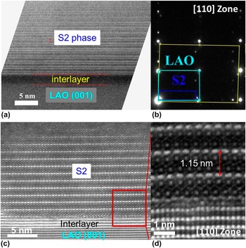
Slightly increasing the growth temperature, pure S2 phase can be obtained, as evidenced by XRD results. Figure 3(a) shows a typical cross-sectional TEM image of S2 phase. An interlayer of ∼2 nm was also observed between S2 phase and LAO substrate. It can be seen that S2 phase has layered structure with a spacing of ∼12 Å. The SAED pattern shows the out-of-plane lattice parameter is 11.5 Å [Fig. 3(b)]. The microstructure of S2 phase has also been investigated by HR-STEM [Fig. 3(c)]. Different from S1 phase, S2 phase exhibits alternative stacking of single Bi layer and Fe–Mn–O triangle slab. It is reasonable that Bi composition in S2 is less than S1 phase as S2 phase is grown at higher growth temperature and lower laser repetition rate. It should be noted that the diffraction data of S2 phase does not fit any of the well-known BFMO phases. Figure 3(d) shows a zoomed portion of the interface. The highly strained interlayer (with c/a = 1.28), is only 3–4 unit cells in thickness. It was reported that tetragonal-like (T-like) BiFeO3 phase grown on LAO and LaSrAlO4 substrates also exhibit a huge c/a ratio (1.2–1.3). Reference Chen, Luo, Huang, Qi, Yang, You, Hu, Wu, Wang, Gao, Sritharan and Chen53–Reference Bea, Dupe, Fusil, Mattana, Jacquet, Warot-Fonrose, Wilhelm, Rogalev, Petit, Cros, Anane, Petroff, Bouzehouane, Geneste, Dkhil, Lisenkov, Ponomareva, Bellaiche, Bibes and Barthelemy55 The T-like BiFeO3 phase with a giant c/a ratio exhibits enhanced room-temperature multiferroicity. Reference Bea, Dupe, Fusil, Mattana, Jacquet, Warot-Fonrose, Wilhelm, Rogalev, Petit, Cros, Anane, Petroff, Bouzehouane, Geneste, Dkhil, Lisenkov, Ponomareva, Bellaiche, Bibes and Barthelemy55 The BFMO interlayer grown on LAO with a high c/a ratio could be a Mn doped T-like BiFeO3 phase. Both theoretical and experimental explorations on this new material are needed.
(a) A cross-sectional TEM overview of the S2 phase on LAO substrate with an interlayer. (b) The corresponding SAED of S2 phase and LAO substrate in the [110] zone axis. (c) A HR-STEM image of S2 phase in the [110] zone axis. (d) The zoomed in HR-STEM image showing the interlayer and S2 phase.

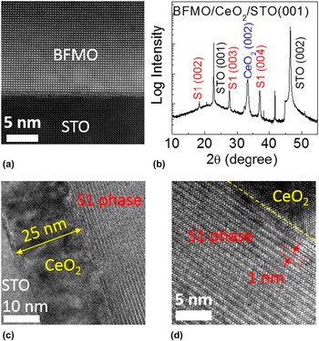
It is interesting to note that films directly grown on STO substrates exhibit a conventional tetragonal Bi2FeMnO6 with double perovskite structure, as reported previously. The out-of-plane lattice parameter of BFMO is determined to be 3.99 Å. The HAADF-STEM image in Fig. 4(a) shows that the BFMO is completely strained to STO substrate. The c/a for BFMO on STO is ∼1.02. Interestingly, as shown in Fig. 4(b), inserting a thin CeO2 buffer layer produces a pure supercell structure with the same diffraction peaks as S1. Figure 4(c) shows the formation of this phase on STO substrate with a 25 nm CeO2 buffer layer. Microstructure analysis shows that this material is the S1 phase grown on LAO substrate [Fig. 4(d)]. The triangle structure of Ce layer provides a template for the growth of S1 phase. Reference Li, Zhang, Khatkhatay, Jian, Fan, Su, Zhu, Chen, Lu, Zhang and Wang21 It was found that S1 phase has much larger growth window on CeO2 buffer layer than the direct growth of S1 phase on LAO. The CeO2 buffer layer provides a broad processing window to grow pure S1 phase. We also found S1 and S2 phases are much resistive than double perovskite BFMO films on STO substrate.
(a) A typical cross-sectional STEM overview of the tetragonal BFMO phase directly grown on STO. (b) The XRD pattern of S1 phase deposited on CeO2 buffered STO substrate. (c) A typical cross-sectional TEM overview showing the overview of S1 phase/CeO2/STO heterostructures. (d) The interface between S1 phase and the CeO2 buffer layer.

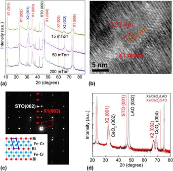
We further explored the film growth by using BiFeO3:BiCrO3 composite targets. Figure 5(a) shows XRD results of films grown at different oxygen pressure, varying from 15 mTorr to 200 mTorr. There are two sets of diffraction peaks. The peaks at 11.53°, 35.06°, 60.28° are defined as X1 phase and peaks at 31.42°, 65.49° are assigned as X2 phase. The out-of-plane lattice parameter is 7.7 Å for X1 phase and 2.84 Å for X2 phase. Mixed phases of X1 and X2 are determined in samples deposited at 15 and 50 mTorr oxygen. Pure X1 phase can be obtained when increasing the oxygen pressure to 200 mTorr. Figure 5(b) shows a typical HRTEM image of X1 phase. The layered structure can be clearly seen. The out-of-plane d-spacing is ∼7.7 Å, agreeing with XRD results. It is interesting that X1 phase shows alternative stacking of Fe–Cr–O triangle slabs and single Bi layer. The diamond diffraction pattern in Fig. 5(c) is stemmed from the neighboring Bi layer, as shown in the inset of Fig. 5(c). The CeO2 buffer layer has been used to explore the growth of BiFeO3:BiCrO3 composite films. Figure 5(d) shows that pure X2 phase can be obtained on both STO and LAO substrate with a thin CeO2 buffer layer. It was found that the growth of pure X2 phase can be obtained in different oxygen pressure, indicating CeO2 buffer layer broadens the growth window for this phase. The triangle template in CeO2 buffer layer can also be the reason for the growth of this X2 phase, similar to the phenomena of S1 phase on CeO2 buffer layer. This result indicates that different materials with potential multiferroicity can be grown by using a composite target composed of two perovskite bismuth compounds. In addition, CeO2 buffer layer can be used as a general template for the growth of materials in BiRO3 (R = Cr, Mn, Fe, Co, Ni). Identifying the detailed crystal structure and compositions of these new materials will be critical for their applications and further studies.
(a) The XRD pattern of X1 and X2 phases deposited directly on STO substrate at different oxygen pressure. (b) A typical cross-sectional TEM image of X1 phase on STO. (c) The corresponding SAED of X1 phase and STO substrate in the [100] zone axis. The inset shows the atomic arrangement of X1 phase. (d) The XRD pattern of pure X1 phase on CeO2 buffered STO and LAO substrates.

IV. CONCLUSION
We explored the thin films with unexpected phases grown using composite BiFeO3:BiMnO3 and BiFeO3:BiCrO3 targets. Bi2FeMnO6 tetragonal phase can often be grown directly on STO substrates, while other phases can be obtained on LAO substrates. A thin layer of CeO2 buffer layer promotes the growth of S1 phase and broadens the growth window for such a phase. The growth of new materials has also been studied using a BiFeO3:BiCrO3 target. The X1 and X2 phases have been grown on STO substrates. Pure X2 phase can be obtained on CeO2 buffered STO and LAO substrates. This work not only demonstrates that unexpected materials can be synthesized by using a composite perovskite BiRO3 (R = Cr, Mn, Fe, Co, Ni) target, but also demonstrate that CeO2 buffer layer can serve as a template for the growth of these materials.
ACKNOWLEDGMENTS
The work at Los Alamos National Laboratory was supported by the NNSA's Laboratory Directed Research and Development Program and was performed, in part, at the Center for Integrated Nanotechnologies, an Office of Science User Facility operated for the U.S. Department of Energy (DOE) Office of Science. Los Alamos National Laboratory, an affirmative action equal opportunity employer, is operated by Los Alamos National Security, LLC, for the National Nuclear Security Administration of the U.S. Department of Energy under contract DE-AC52-06NA25396. The work at Texas A&M and Purdue University is funded by the Office of Naval Research N00014-15-1-2362 (Texas A&M) and N00014-16-1-2465 (Purdue). The TEM work is funded by the U.S. National Science Foundation (DMR-1565822).