










Introduction
An earlier version of this work was presented at the 55th European Microwave Conference (EuMW, 2025) and published in its Proceedings [Reference Faliero, Quint, Valenziano, Bekker, Zwick and Bhutani1]. That paper introduced the preliminary analysis and design and electromagnetic analysis of a borosilicate glass pyramidal inverted dielectric resonator antenna (PIGRA) for sub-terahertz (sub-THz) applications (Figure 1). The present paper significantly extends the preliminary work by presenting the complete design, fabrication, and experimental validation of a  $4\times4$ PIGRA array operating across the entire D-band (Figure 2).
The limited availability of radio frequency (RF) spectrum and the increasing demand for higher data rates have driven research toward frequencies beyond  $100\,\mathrm{GHz}$. The 110–170 GHz frequency range (D-band) is considered a promising candidate for future wireless communications (6G and beyond), as well as for autonomous driving, radar, and sensing applications, due to its large available bandwidth and high level of technology readiness [Reference Jung, Park, Kwon, Seo, Ahn, Wi and Na2]. At millimeter-wave (mmWave) frequencies, enabling capabilities such as high data rates, massive MIMO (Multi Input Multi Output), high resolution, and high integration density become feasible [Reference Lee, Lee, Zhang, Hong and Ghalichechian3].
Semiconductor technologies have demonstrated transistors with maximum oscillation frequencies exceeding  $600\,\mathrm{GHz}$ [Reference Maiwald, Li, Hotopan, Kolb, Disch, Potschka, Haag, Dietz, Debaillie, Zwick, Aufinger, Ferling, Weigel and Visweswaran4]. However, as the operating frequency increases, conductor ohmic losses rise significantly, fabrication tolerances become more stringent, and system integration becomes more challenging. Consequently, the losses associated with transceiver–antenna interconnect increase, while the radiation efficiency of metallic antennas degrades rapidly.
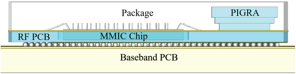
As discussed in [Reference Faliero, Quint, Valenziano, Bekker, Zwick and Bhutani1], the antenna-in-package (AiP) concept aims to mitigate interconnection losses by reducing the distance between the transceiver chip and the antenna (Figure 3), while facilitating system integration and mass-production manufacturability [Reference Hyltin5–Reference Zhang and Liu7].
Dielectric resonator antennas (DRAs) do not suffer from ohmic losses and offer compact size, low thermal expansion, and high radiation efficiency due to the absence of metallic radiating elements, although they typically provide low-to-moderate gain [Reference Petosa and Ittipiboon8]. Employing DRAs in array configurations increases the effective isotropic radiated power by enhancing antenna gain, thereby compensating for the significant path loss encountered at mmWave frequencies [Reference Koch, Schönecker, Kohl, Breun, Weigel and Franchi9]. Dielectric resonators [Reference Richtmyer10] made of low-loss ( $\tan\delta\approx10^{-3}$) and high-permittivity (
 $ \epsilon_r \gt 30$ [Reference Nomura11]) dielectric material have been used in microwave circuitry for decades as high-Q filter components [Reference Cohn12]. Conversely, DRAs require a relatively low Q-factor to achieve wider impedance bandwidths [Reference Van Bladel13–Reference Guillon15]. Typical DRAs provide impedance bandwidths of approximately 30%, which are insufficient to cover the entire D-band, while the realized gain of single resonator operating in its fundamental mode is generally below
 $6\,\mathrm{dBi}$, with a small resonator operating around the lowest mode [Reference Petosa and Ittipiboon8, Reference Keyrouz and Caratelli24]. Different techniques have been reported to enhance the operating bandwidth [Reference Petosa, Ittipiboon, Antar, Roscoe and Cuhaci16], including stacking multiple resonators [Reference Smith and Mayes17–Reference Luk, Leung and Chow19], reducing the dielectric permittivity, employing different resonator geometries [Reference Petosa, Ittipiboon, Antar, Roscoe and Cuhaci16, Reference Lapierre, Antar, Ittipiboon and Petosa20], introducing parasitic radiators [Reference Simons and Lee21], using frequency selective surface superstrates [Reference Kakhki, Mousavirazi and Denidni22], and incorporating surface-mounted horn [Reference Nasimuddin and Esselle23].
Pyramidal inverted glass resonator on glass PCB.

Pyramidal inverted glass resonator on glass PCB.

PIGRA MMIC package concept.

In this paper, a wideband glass-based pyramidal inverted resonator antenna is proposed as the radiating element of a D-band planar antenna array, as shown in Figure 2. The proposed radiating element is intended for integration into a monolithic microwave integrated circuit (MMIC) package for mmWave applications (Figure 3). The PIGRA exhibits an intrinsic impedance bandwidth exceeding 40% (for  $|S_{11}|\leq-10\,\mathrm{dB}$) covering the entire D-band. The wide bandwidth is achieved mainly by the tapered vertical cross-section, which enables the excitation of multiple resonant modes over the operating frequency range.
For this design, Schott Borofloat 33 (BF33) borosilicate glass was selected as the material for manufacturing the PIGRA due to its suitable electromagnetic properties. BF33 exhibits a relative permittivity ( $\epsilon_r$) of 4.4 and a loss tangent tan
 $\delta$ = 0.018 at D-band frequencies. The PIGRA was designed and optimized on a glass-based PCB substrate with a relative permittivity of
 $\epsilon_r=6.5$. The proposed concept is demonstrated through two implementations. The single-radiator design was implemented as a glass-on-glass (GoG) solution to demonstrate the feasibility of integrating the proposed PIGRA into an MMIC package, as illustrated in Figure 3. The PIGRA was fabricated using laser-induced deep etching (LIDE) technology, and the glass PCB substrate was metallized using physical vapor deposition (PVD) followed by an electroplating process.
The PIGRA is fed by a coplanar waveguide (CPW) and excited through a slot-coupling technique at the PIGRA–PCB interface on the base side (Figure 7). The dimensions of the CPW feed line and the coupling slot were optimized to minimize insertion loss while maximizing the antenna impedance matching performance. The second implementation is a  $4\times4$ planar array fabricated on a two-layer Rogers CLTE substrate. The 16 PIGRA elements are excited in phase through a slot-coupled feeding technique, using a microstrip line structure (Figures 8 and 9). To facilitate integration with other front-end components, such as amplifiers, phase shifters, filters, transceivers, and RF test probes, which typically employ ground-signal-ground (GSG) pads with 100 or 150 µm pitch, a low-loss wideband CPW-to-microstrip transition was designed (Figure 8, label ①). The microstrip feed network distributes the input signal through 15 Wilkinson power dividers, providing a 1-to-16 equal-power split, with minimized loss. The resulting array achieves a peak realized gain of
 $15\,\mathrm{dBi}$ while maintaining a
 $-10\,\mathrm{dB}$ impedance bandwidth across the D-band under a
 $50\,{\Omega}$ system impedance.
A probe-based antenna measurement (Figure 14) at Karlsruhe Institute of Technology (KIT) was used to evaluate the RF performance of both designs. The antenna measurement system is a far-field single-probe antenna measurement system, capable of measurements up to  $325\,\mathrm{GHz}$ [Reference Beer and Zwick25].
The main contributions of this work are summarized as follows:
• A novel glass-based pyramidal inverted DRA enabling ultra-wideband D-band operation.
• A GoG single-element demonstrator suitable for AiP integration.
• A low-loss
 $4\times4$ array incorporating an integrated CPW-to-microstrip transition and Wilkinson feed network.
• Experimental validation of both implementations, demonstrating more than 40% impedance bandwidth and a peak realized gain of
$15\,\mathrm{dBi}$.


The paper is organized as follows. The second section details the design of the PIGRA, starting with the single-element analysis and extending it to a  $4\times4$ array configuration. The third section presents the manufacturing and assembly procedures. The fourth section reports the simulated and measured performance of both implementations, namely the single-element GoG and the array configuration. The fifth section concludes the paper.
Design
PIGRA on glass PCB
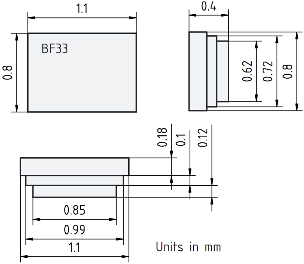
The PIGRA is a single-piece BF33 glass DRA consisting of three stacked rectangular cuboids that form an inverted pyramidal geometry (Figure 4). The smaller base is attached to the PCB, as illustrated in Figures 1 and 2(a).
Proposed PIGRA geometry and dimensions.

Figure 4 Long description
Three views of a BF33 glass dielectric resonator antenna with dimensions in millimeters are presented. The top left view shows a rectangle labeled BF33 with a width of 1.1 millimeters and a height of 0.8 millimeters. The top right view is a side view with a total length of 0.4 millimeters, showing three stacked sections with heights of 0.62 millimeters, 0.72 millimeters and 0.8 millimeters. The bottom view is a cross-section with a total width of 1.1 millimeters, showing three layers with widths of 0.85 millimeters, 0.99 millimeters and 1.1 millimeters. Additional measurements include 0.18 millimeters, 0.1 millimeters and 0.12 millimeters for specific sections. The text ′Units in mm′ is displayed at the bottom right of the diagram.
To determine the dimensions of the PIGRA, the design begins with the analysis of an equivalent rectangular dielectric resonator antenna (RDRA). The resonator height is constrained by the available glass slab thickness of  $0.5\,\mathrm{mm}$, which is subsequently reduced to
 $0.4\,\mathrm{mm}$ through the LIDE process.
The RDRA is a well-studied structure [Reference Petosa and Ittipiboon8] whose resonant characteristics can be estimated using the dielectric waveguide model (DWM) [Reference Marcatili27] or through the transverse resonance technique [Reference Felsen and Marcuvitz29, Reference Sorrentino and Mongiardo30], and subsequently verified through full-wave eigenmode analysis [Reference Pozar28]. According to DWM, an RDRA is typically designed such that its first three or four resonant modes lie within the desired operating frequency band [Reference Mongia and Ittipiboon26]. The inverted pyramidal geometry of the PIGRA is then derived from the equivalent RDRA to support the excitation of multiple resonant modes over the frequency range, thereby enhancing the impedance bandwidth without increasing the antenna footprint.
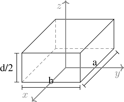
Illustration of the RDRA on a metal ground plane.

The DWM is applied to the geometry illustrated in (Figure 5). In this model, the resonator has dimensions  ${a}$,
 ${b}$, and
 ${d/2}$, which represent the width, length, and height of the dielectric resonator on a metal ground, respectively. The equivalent isolated dielectric resonator [Reference Mongia and Ittipiboon26] has the dimensions
 ${a}$,
 ${b}$, and
 ${d}$. To determine the resonant modes, the analysis assumes perfect magnetic wall (PMW) boundary conditions on the vertical faces (
 ${x} = \pm a/2$,
 ${y} = \pm b/2$) of the resonator, while a perfect electric wall, representing the metal ground, and open boundary conditions are applied to the remaining faces (
 ${z}$ = 0 and
 ${z = d/2}$, respectively). Under the PMW assumption, the boundary conditions for the vertical faces are given by
 \begin{equation}
PMW:
\begin{cases}
\mathbf{E}\cdot\mathbf{u}=0, \\
\mathbf{H}\times\mathbf{u}=0,
\end{cases}
\end{equation}
where  $\mathbf{E}$,
 $\mathbf{H}$, and
 $\mathbf{u}$ denote the electric field, magnetic field, and the normal vector to the corresponding faces, respectively. Consequently, the eigenvalues problem yields the transverse wavenumbers
 \begin{equation}
k_x=m\pi/a, k_y=n\pi/b,
\end{equation}
where  ${m}$ and
 ${n}$ are the modal indices. By considering an equivalent transmission line (ETL) along
 ${z}$, the transverse admittance resonance condition (
 $Y_t=\overleftarrow{Y_t}+\overrightarrow{Y_t} =0$), together with the dispersion equation (
 $\mathbf{k}\cdot\mathbf{k}=~\omega^2\epsilon\mu$), results in the following transcendental equation [Reference Felsen and Marcuvitz29, Reference Sorrentino and Mongiardo30]:
 \begin{equation}
k_z \tan(k_z d/2) = \sqrt{(\epsilon_r-1)k_0^2-k_z^2}
\end{equation}
The solutions of (3) correspond to the resonance conditions of the ETL and, consequently, to the resonant frequencies associated with the mode  $TE^z_{mn\delta}$ family. However, the electric field can be decomposed along three orthogonal directions (
 ${\textstyle x,y,z}$), giving rise to transverse modes along each of the three dimensions (
 $TE^x$,
 $TE^y$,
 $TE^z$) [Reference Mongia and Ittipiboon26]. The estimated resonance frequency of the fundamental (
 $TE^z_{11\delta}$) mode is approximately
 $129\,\mathrm{GHz}$, using a relative permittivity
 $\epsilon_r = 4.5$ and dimensions
 ${\textstyle a = 1.25}$ mm,
 ${\textstyle b = 0.8}$ mm, and
 ${\textstyle d/2 = 0.5}$ mm. Since the isolated resonator [Reference Mongia and Ittipiboon26] satisfies
 ${\textstyle a \gt d \gt b}$, rather than the
 ${\textstyle a \gt b \gt d}$ condition considered by Marcatili [Reference Marcatili27], the classical modal ordering is not directly applicable. Therefore, the resonant modes are identified using the DWM and subsequently confirmed by full-wave eigenmode analysis in CST Microwave Studio.
PIGRA electric- and magnetic-field distributions.

Figure 6 Long description
Two vector field plots display electric and magnetic field distributions over a stepped rectangular cross-sectional geometry. Both plots share a common magnitude color scale ranging from 0 to minus 30 decibels. A small axis triad is visible in the lower right of each plot for spatial orientation. The electric field distribution corresponds to the TE superscript y subscript 1 delta 1 mode. Field vectors are distributed across the entire stepped rectangular region. Stronger magnitudes, shown near 0 decibels, are concentrated along the lateral sidewalls and the stepped corners of the structure. Weaker magnitudes, approaching minus 30 decibels, appear in the central interior region. The vectors near the top surface point predominantly in one direction, while those near the base and step regions show curling or diverging orientations. The magnetic field distribution corresponds to the TM superscript y subscript 2 delta 1 mode. Field vectors show a noticeably different spatial arrangement compared to the electric field plot. Higher magnitudes are observed along the top surface and outer lateral edges. The central cavity region shows reduced magnitude. Vectors near the stepped shoulders and lower corners exhibit a more pronounced rotational pattern. The two plots differ in the spatial location of their peak magnitude regions and in the directional orientation of their vectors, with the electric field plot showing stronger edge concentrations at the lateral sidewalls and the magnetic field plot showing stronger concentrations along the top surface and upper corners.
According to Stevenson [Reference Stevenson31] and Van Bladel [Reference Van Bladel32], not all resonant modes of an electrically small dielectric resonator contribute to radiation. For resonators characterized by high relative permittivity and a geometry of revolution, only specific resonant modes are capable of radiating efficiently, whereas other modes remain predominantly confined within the dielectric material. As the dielectric permittivity decreases, resonant modes become less well defined, and hybrid modes may appear [Reference Chen and Zaki33]. Therefore, resonators made of low-permittivity materials are preferable for antenna applications.
Since the PIGRA utilizes a low-permittivity glass with  $\epsilon_r = 4.5$, and its geometry is not a solid of revolution, fully confined modes are not supported. Finite element method eigenmode analysis indicates that a conventional rectangular DRA of equivalent volume supports only three to four modes within the operating band, as illustrated in Table 1. The first RDRA mode is approximately
 $7\,\mathrm{GHz}$ higher than the analytical prediction. The first five resonant modes of the PIGRA, listed in Table 1, are distributed across the operating bandwidth and exhibit quasi-transverse field characteristics. This demonstrates that the PIGRA mode distribution across the operating band was optimized by tuning its cross-sectional profile. The electric field distribution of the first and second modes is shown in Figure 6, and the properties of the first five modes are summarized in Table 1. The fundamental
 $TE^y_{1\delta1}$ mode can be modeled as a set of in-phase y-directed magnetic dipoles on the lateral faces (
 ${x} = \pm a/2$), together with a y-directed electric dipole near the PIGRA base (
 ${\textstyle z} = 0$). However, only the magnetic dipole associated to
 $TE^y_{1\delta1}$ mode contributes to radiation, while the electric dipole is suppressed due to cancellation by its ideal image in the conducting ground plane. The second mode (
 $TE_{2\delta 1}^{y}$) can be represented by a magnetic current ribbon flowing around the lateral faces of the PIGRA. This distribution corresponds to a combination of a
 $z$-directed magnetic dipole and a
 $z$-directed electric dipole.
The slot-aperture coupling technique (Figure 7) is utilized to excite the PIGRA through a  $50\,{\Omega}$ CPW line on a single-layer glass PCB. The slot geometry is optimized to match the input impedance of the PIGRA to the characteristic impedance of the CPW line. The slot length is approximately a half-wavelength in glass at
 $120\,\mathrm{GHz}$. All geometric measured parameters are summarized in Figure 4, Figure 7, and Table 2. At the PCB edge, the CPW line is tapered to match the GSG probe pitch of 100 µm. The PCB thickness
 ${h}$ was selected to be
 $0.1\,\mathrm{mm}$ to suppress the excitation of surface-wave modes [Reference Pozar28] within the operating band. For a grounded dielectric substrate, the cutoff condition for the first surface mode is given by
 \begin{equation}
h \lt \lambda_0/(4\sqrt{\epsilon_r-1}), \quad for \quad TE_1
\end{equation}
where  $\lambda_{0}$ is the free-space wavelength and
 $\epsilon_r = 6.5$ is the substrate relative permittivity, with a measured relative permittivity of
 $\epsilon_r = 6.5$ and a
 $\tan \delta$ of 0.02. With the fixed CPW height, the CPW width-to-gap ratio was optimized to match
 $50\,{\Omega}$ subject to the constraint that the minimum gap is set by the laser beam width of the manufacturing machine, which is around 20 µm at the focal point. The PCB metallized layer was modeled with a conductivity of
 $\sigma=4\times10^{7}\ \mathrm{S/m}$, which corresponds to approximately
 $70\,\mathrm{\%}$ of the conductivity of annealed copper.
Another parameter affecting the antenna impedance and, consequently, the gain is the adhesive layer thickness at the PIGRA–PCB interface, together with the CPW gap. The glue thickness was simulated in the range of 5–10 µm, and the best S-parameter performance is observed at around 7 µm. This is attributed to the adhesive shrinkage during assembly and curing, which requires process optimization by adjusting the initial glue thickness, the applied assembly force during the resonator placement, and the thermal shrinkage during curing. Such optimization is compatible with mass-production processes.
Eigenmodes of R-DRA and PIGRA

Table 1 Long description
Mode numbers 1 through 6 list frequencies in gigahertz for two columns labeled RDRA and PIGRA, plus a Type label for each mode. Mode 1 reports RDRA 136.0 gigahertz and PIGRA 126.2 gigahertz, Type TE with superscript y and subscript 1 delta 1. Mode 2 reports RDRA 145.0 gigahertz and PIGRA 127.6 gigahertz, Type TE with superscript y and subscript 2 delta 1. Mode 3 reports RDRA 170.4 gigahertz and PIGRA 133.3 gigahertz, Type TM with superscript y and subscript 2 delta 1. Mode 4 reports RDRA 194.5 gigahertz and PIGRA 166.2 gigahertz, Type TE with superscript y and subscript 1 delta 2. Mode 5 has no RDRA value and lists PIGRA 167.2 gigahertz, Type TM with superscript y and subscript 3 delta 1. Mode 6 has no RDRA value and lists PIGRA 178.5 gigahertz, Type HEM with superscript y.
Single-radiator BF33 PCB dimensions.

Figure 7 Long description
A dimensioned geometry drawing specifies a glass layer and a copper pattern with a central feed shape and a labeled slot, with the note, Units in mm. At the top, a rectangular strip is labeled, Glass dash epsilon subscript r equals 6.5, with a horizontal dimension marked 2.8 and a vertical thickness marked 0.1. Below that, a square copper region is shown with the word, Copper, near the upper middle and the outer boundary is dimensioned 2.8 by 2.8. Inside the copper region, the text, Slot, appears inside a circular outline near the left side and a narrow vertical feature runs downward near the center, starting from a short horizontal bar at the top of the feature. That top bar is dimensioned 0.5 across. To the right of the top bar, a vertical dimension marked 0.09 is shown. Farther down on the right side of the central feature, a vertical dimension marked 0.25 is shown and near the lower right edge of the copper region a vertical dimension marked 0.12 is shown. Near the bottom of the central feature, a short horizontal dimension marked 0.025 is shown at the narrowest section. Along the bottom edge, a horizontal dimension marked 0.09 is shown near the center and another horizontal dimension marked 0.025 is shown near the bottom center aligned with the narrow section of the central feature.
Measured dimensions in mm

Table 2 Long description
Dimensions are listed in millimeters for parts with columns for length, width, and height, followed by a second set of rows with columns for length, width, and gap. For pigra, length is 1.10, width is 0.80, and height is 0.41. For pcb, length is 2.80, width is 2.80, and height is 0.10. In the section with a gap column, cpw has length 1.38, width 0.30, and gap 0.025. Cpw at probe has length 0.125, width 0.08, and gap 0.025. Slot has length 0.50, width 0.09, and the gap entry is a hyphen.
$4\times4$ planar array on Rogers CLTE PCB

The array implementation is based on the previously designed single radiating element (PIGRA). The array design begins with the selection of the array topology. A planar square array is adopted because it provides high directivity and aperture efficiency while maintaining a compact and symmetric layout (Figures 8 and 9). The symmetric configuration facilitates the design of a low-loss, equal-path feed network for all 16 radiating elements, ensuring uniform amplitude and phase excitation. In addition, the regular element spacing provides stable radiation characteristics and low side-lobe levels across the operating frequency band. A  $4\times4$ rectangular array configuration is selected with an element spacing of
 $1.30\,\mathrm{mm}$, which corresponds to 0.61
 $\textstyle{\lambda_{0}}$ spacing at the center frequency band (
 $140\,\mathrm{GHz}$). Under uniform amplitude and phase excitation, this configuration theoretically provides an array gain (array gain factor) increase of
 $12\,\mathrm{dB}$ compared with a single PIGRA element. The element spacing was selected as a trade-off between aperture efficiency, mutual coupling, and the requirement of keeping the inter-element spacing below one free-space wavelength (
 $\lambda_0$) to suppress grating lobes. This corresponds to an inter-element spacing of 0.61
 $\textstyle{\lambda_{0}}$, which allows a potential scanning angle of approximately
 $\pm40^\circ$, according to
 \begin{equation}
\theta_{\max}=\arcsin\left(\frac{\lambda_0}{d}-1\right).
\end{equation}
The feed network was designed on a Rogers CLTE substrate with a thickness of 76.2 µm, a relative permittivity of 2.98, and a loss tangent ( $\tan\delta$) of 0.0021. The CLTE substrate incorporates two copper layers, each with a thickness of 17.5 µm. The overall board dimensions are
 $7\,\mathrm{mm}$ by
 $8\,\mathrm{mm}$. The radiating elements are coupled to the microstrip feed network through slot apertures (Figures 8 and 9). The objective of the feed network illustrated in Figure 8 is to distribute the RF signal from the GSG probe pads with a pitch of 100 µm to the 16 coupling slots, while minimizing the network loss over the operating bandwidth and maintaining equal electrical path lengths. The microstrip feed network begins with a novel broadband via-less CPW-to-microstrip transition (Figure 8, label ①), designed to match the GSG probe pitch. This transition was optimized using a back-to-back configuration over the operating band with a reference impedance of
 $50\,{\Omega}$. The RF signal is equally divided into 16 lines using 15 broadband Wilkinson power dividers. The impedance matching within the feed network is achieved using quarter-wave (
 $\lambda$/4) impedance transformers (labels ② and ④), multi-section matching transformers (label ③), and tapered transmission-line sections (labels ④ and ⑥) to minimize feed-network loss. No higher-order modes or mode conversion associated with the CPW-to-microstrip transition were observed, due to the tight coupling between the ground pads and the signal line. The ground-to-signal gap is 18 µm. The coupling slots are 20 µm wider than the single-element design (0.52 vs
 $0.5\,\mathrm{mm}$).
PCB bottom-layer feed network of the  $4\times4$ array.

Figure 8 Long description
A four by four planar array on a Rogers CLTE substrate. The array consists of 16 elements arranged in a grid pattern. At the bottom center, a feed line labeled ′1′ connects to a central junction labeled ′2′. From this junction, lines extend upwards and branch out to connect to additional junctions labeled ′3′, ′4′ and ′5′. Each of these junctions further branches out to connect to the individual elements of the array. The elements are connected in a symmetrical pattern, with lines labeled ′6′ extending to the topmost elements. The entire structure is made of copper and dimensions are provided in millimeters. The overall width is labeled as ′8′ and the height is ′7′. The schematic includes detailed measurements for various sections, such as ′3.9′, ′1.3′ and ′2.6′, indicating specific distances between components.
PIGRA element arrangement on the PCB top-layer of the  $4\times4$ array.

Figure 9 Long description
A four by four PIGRA array on a printed circuit board. Each element in the array is represented by a rectangle with internal lines, indicating the layout of the PIGRA elements. The elements are arranged in a grid with equal spacing. The dimensions are marked as 1.3 millimeters between elements horizontally and vertically, with a smaller spacing of 0.15 millimeters indicated on the right side. The entire array is labeled as being made of copper. A slot is marked at the bottom left and the term PIGRA is labeled on the right side. The units are specified as millimeters.
Manufacturing and assembly
The BF33 PIGRA is manufactured using the LID process developed by LPKF. The BF33 glass sheet has an initial thickness of  $0.5\,\mathrm{mm}$ and is reduced to
 $0.4\,\mathrm{mm}$ after the chemical etching, laser ablation, and polishing process. PIGRA measured height was
 $0.41\,\mathrm{mm}$, with a top surface measuring
 $1.10\,\mathrm{mm}$
 $\times$
 $0.80\,\mathrm{mm}$. The glass dielectric resonator manufacturing process is shown in Figure 10(a). The steps are: material preparation, laser ablation and wet etching, and final cleaning.
PIGRA manufacturing process (a), glass PCB fabrication (b), and assembly process (c).

Figure 10 Long description
Three diagrams labeled (a), (b) and (c). (a) The PIGRA manufacturing process includes: - Material preparation (cleaning) - Laser (LIDE from LPKF) - Wet Etching (LIDE from LPKF) (b) The glass PCB fabrication process includes: - Material preparation (cleaning) - First Metallization/Sputtering (50/50 nm Nickel/Copper) - Second Metallization/EP Developing (~2 micrometers Copper) - Cutting (c) The assembly process includes: - DAF Cutting (Prepreg/Panel) - Placing DAF (Prepreg/Panel) - Placing DRA (Prepreg/Panel) - Curing.
PIGRA assembled on a PVD-metallized and patterned 100 µm glass substrate.

The single radiator GoG (Figure 11) implementation employs a glass substrate with a permittivity of 6.5 ( $tan\delta$ = 0.003), a roughness of approximately
 $1\,\mathrm{nm}$, and a thickness of
 $0.1\,\mathrm{mm}$. The glass substrate is coated through a two-step metallization process. The first step utilizes PVD of copper on a nickel adhesion layer of approximately
 $10\,\mathrm{nm}$, with a final total thickness of approximately
 $100\,\mathrm{nm}$. Since the skin depth at D-band frequency is approximately of
 $190\,\mathrm{nm}$, a second metallization step is required to increase the conductor thickness and consequently to reduce conductor loss. Electroplating is subsequently performed, where an electric current reduces the dissolved copper ions to build a uniform metal coating on the previously sputtered glass substrate, which acts as the electrode in the copper bath. The metallized glass substrate is structured with a CPW transmission line ending with the PIGRA feeding slot, and laser-cut with a conventional laser machine. The laser machine has a laser spot diameter of 20 µm at the focal point. The glass substrate manufacturing process at KIT is shown in Figure 10(b). The PCB and PIGRA are assembled at KIT using a die attach foil, AFN303, from Furukawa, with a pre-cured thickness of 10 µm and a permittivity in the range of 2.0–2.2. The Finetech Fineplacer Pico is utilized for this operation. The assembled sample is cured for one hour at
 $120^\circ\mathrm{C}$ (Figure 10(c)).
Fabricated  $4\times4$ array sample on a Rogers CLTE 76 µm PCB.

The  $4\times4$ PIGRA array (Figure 12) on a Rogers CLTE PCB follows a similar manufacturing and assembly process. Unlike the GoG implementation, the Rogers CLTE PCB is supplied with two pre-metallized copper layers, eliminating the need for the PVD and electroplating processes. Small alignment errors were observed during the assembly of the PIGRA onto the PCB.
Simulation and measurements results
The GoG PIGRA concept and the  $4\times4$ array were simulated using CST Microwave Studio. The finite-difference time-domain solver with a hexahedral mesh was used. The simulation models consisted of approximately 1.2 and 68 million mesh cells for the single radiator and array, respectively. The radiation characteristics were measured at the KIT mmWave laboratory using a spherical single-probe-based antenna measurement system (Figure 14) [Reference Beer and Zwick25]. The system is based on a Keysight PNA-X N5242B vector network analyzer with a N5261A mmWave controller, a VDI WR6.5-VNAX D-band frequency extender, and a GGB Industries 170-GSG-100-BT-M probe. Measurements were performed under far-field conditions. For the antenna under test (AUT) dimensions of
 $7\,\mathrm{mm}$
 $\times$
 $8\,\mathrm{mm}$ (maximum dimension
 $D\,=\,8\,\mathrm{mm}$, neglecting the GSG probe influence), the Fraunhofer distance at
 $140\,\mathrm{GHz}$ (
 $\lambda_0=2.14\,\mathrm{mm}$) is
 \begin{equation}
R_{\mathrm{FF}} \geq \frac{2D^2}{\lambda_0},
\end{equation}
 \begin{equation}
R_{\mathrm{FF}}
\geq
\frac{2(8\,\mathrm{mm})^2}
{2.14\,\mathrm{mm}}
\approx
59.8\,\mathrm{mm}
\approx
60\,\mathrm{mm}.
\end{equation}
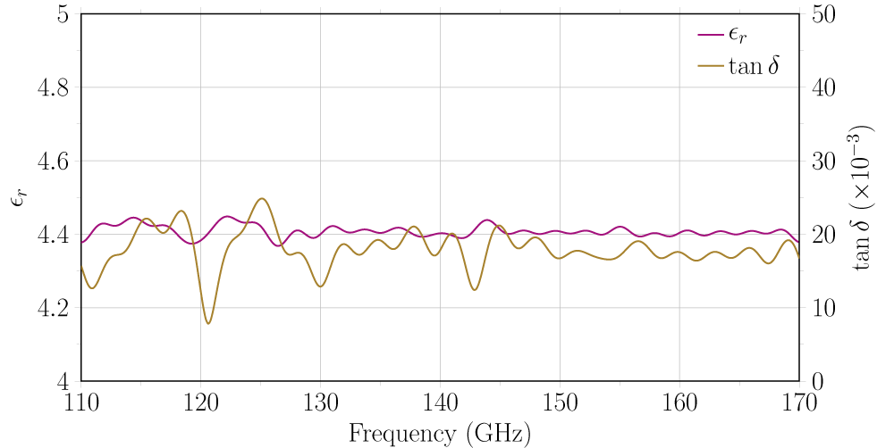
Measured dielectric properties of a  $0.5\,\mathrm{mm}$ BF33 glass sample.

mmWave antenna measurement setup at KIT.

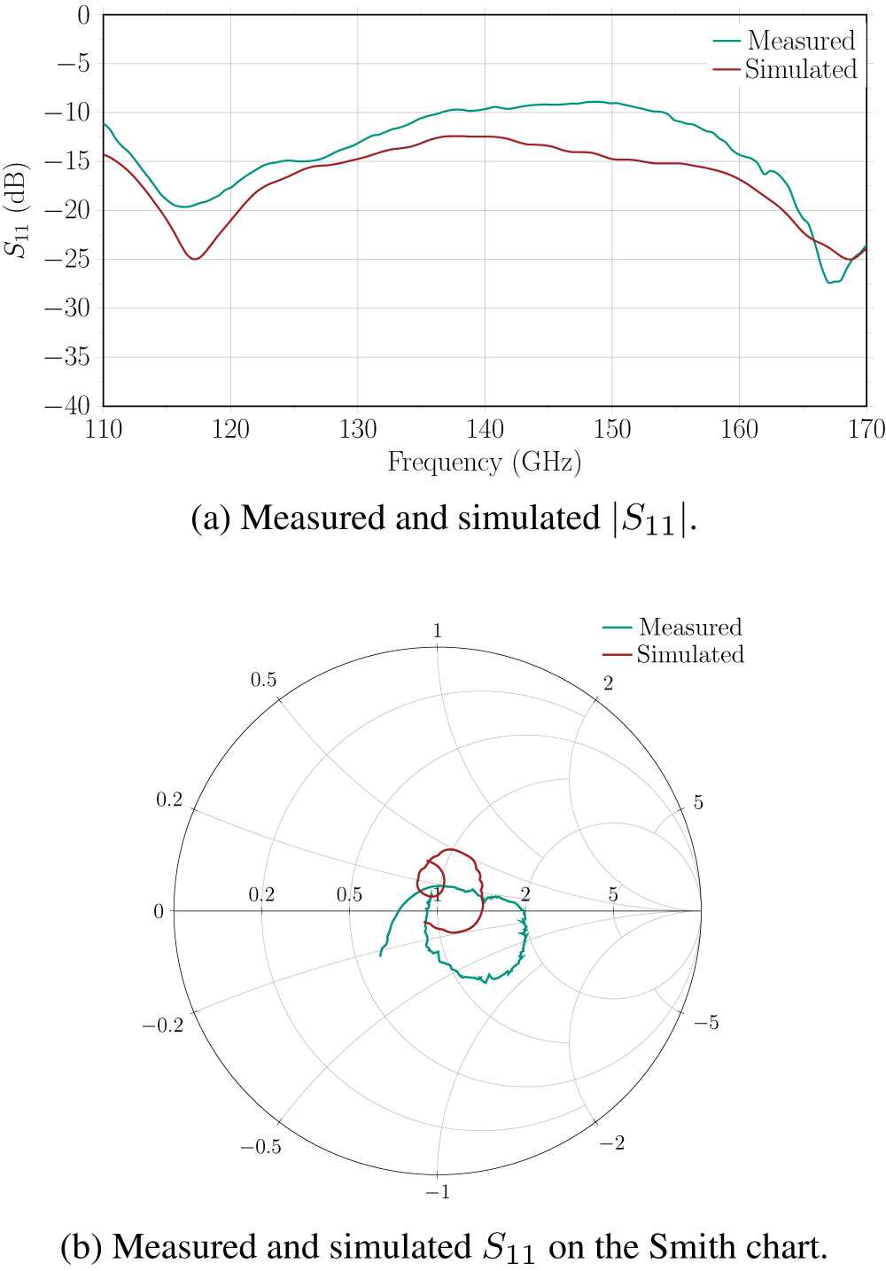
Comparison between measured and simulated reflection coefficient of the single PIGRA radiator.

Figure 15 Long description
The line graph in image A has two curves and a legend listing, Measured and, Simulated. The x-axis label is, Frequency, with unit, gigahertz, ranging from 110 to 170 with ticks at 110, 120, 130, 140, 150, 160 and 170. The y-axis label is, S subscript 11, with unit, decibel, ranging from 0 to minus 40 with ticks at 0, minus 5, minus 10, minus 15, minus 20, minus 25, minus 30, minus 35 and minus 40. The Measured curve starts near minus 12 decibel at 110 gigahertz, drops to about minus 20 decibel near 115 gigahertz, rises to about minus 15 decibel near 122 gigahertz, rises further to about minus 10 decibel near 138 to 140 gigahertz, stays near minus 10 decibel through about 150 gigahertz, then decreases to about minus 15 decibel near 160 gigahertz, drops to about minus 27 decibel near 166 to 167 gigahertz and ends near minus 24 decibel at 170 gigahertz. The Simulated curve starts near minus 15 decibel at 110 gigahertz, drops to about minus 25 decibel near 116 to 117 gigahertz, rises to about minus 16 decibel near 125 gigahertz, rises to about minus 13 decibel near 138 to 140 gigahertz, then gradually decreases to about minus 15 decibel near 150 gigahertz, to about minus 17 decibel near 160 gigahertz and ends near minus 24 decibel at 170 gigahertz. The Smith chart in image B has two traces and a legend listing, Measured and, Simulated. The chart has a circular boundary with internal arcs and radial lines. Numeric labels visible on the chart include 0, 0.2, 0.5, 1, 2 and 5 and negative labels including minus 0.2, minus 0.5, minus 1, minus 2 and minus 5. The Measured trace forms a larger loop below the horizontal centerline, crossing near the center and extending toward the lower right region before returning toward the center. The Simulated trace forms a smaller loop above the horizontal centerline, centered near the middle of the chart and returns to a point near where it started.
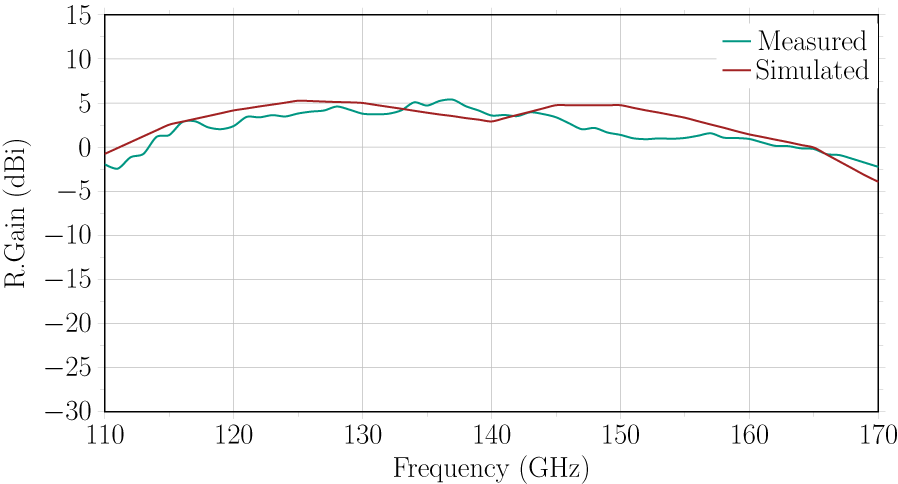
Measured and simulated realized gain of the single PIGRA.

Since the distance between the probe antenna and the AUT is  $700\,\mathrm{mm}$, the far-field criterion was satisfied. Gain calibration was performed using the gain substitution method [Reference Kanda35] with two standard WR6 horn antennas from Mi-Wave. A one-port on-wafer SOL calibration was carried out using a GGB Industries CS-15 calibration substrate. The AUT was supported by a low-permittivity polymethacrylimide (ROHACELL 51) foam sheet to minimize its influence on the radiation performance.
During the design phase, it was necessary to characterize the BF33 material for an accurate design. The material’s dielectric characterization was performed using the Swissto12 Material Characterization Kit, which uses a circular waveguide technique. The material samples were placed between the circular tapered waveguide sections. The measured BF33 relative permittivity and loss tangent ( $tan\delta$) are approximately 4.4 and 0.02, respectively (Figure 13).
The measured and simulated S-parameters and Smith chart are shown in Figure 15. The  $-10\,\mathrm{dB}$ impedance bandwidth clearly covers the whole D-band, with minor deterioration at the center of the frequency band. The two return-loss minima are around 118 and
 $167\,\mathrm{GHz}$. The simulated and measured
 $S_{11}$ show good agreement, with a slightly worse impedance matching level around
 $150\,\mathrm{GHz}$. The measured Smith chart (Figure 15(b)) shows two under-coupled resonances around 167 and at
 $135\,\mathrm{GHz}$, which are linked to the first and the third resonant mode. The resonance coupling depends on the relative PIGRA positioning over the feeding slot and the feeding slot size due to the mechanical tolerances. The measured and simulated vertically polarized far-field radiation patterns at
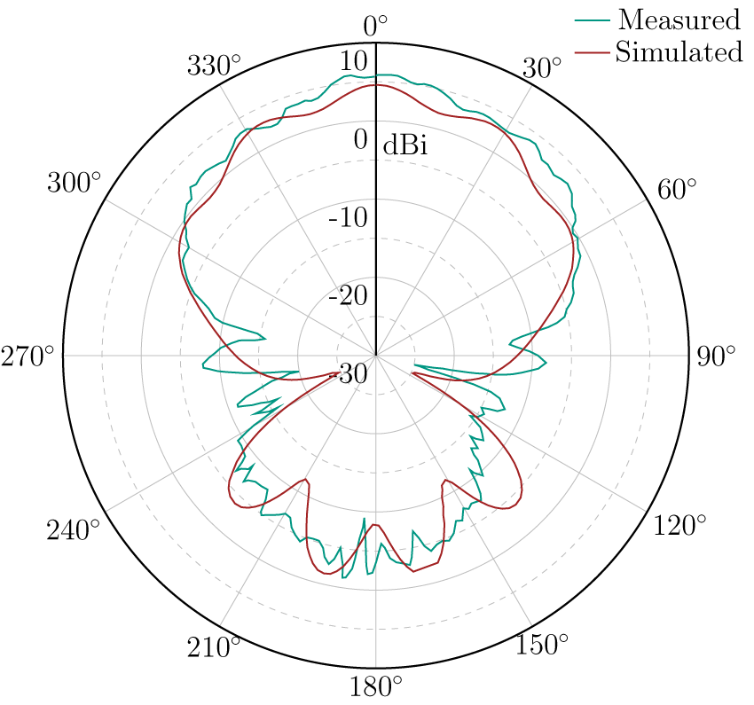
 $138\,\mathrm{GHz}$ are shown in Figure 17. The main beam is directed towards broadside (zenith
 ${\textstyle +z}$) with a half-power beamwidth of approximately
 $60^\circ$. Minor ripples in the main lobe are primarily attributed to scattering from the PCB edges. The simulated efficiency exceeds
 $-0.8\,\mathrm{dB}$ (
 $83\,\mathrm{\%}$) throughout the operating band. In Figure 16, the PIGRA realized gain in the zenith direction (+Z axis) is shown. The peak gain is approximately
 $5.8\,\mathrm{dBi}$ at
 $135\,\mathrm{GHz}$, including GSG-to-CPWG and CPWG line losses. The gain decreases toward the D-band edges due to the frequency-dependent shift of the radiation-pattern peak. The measured and simulated performance of the
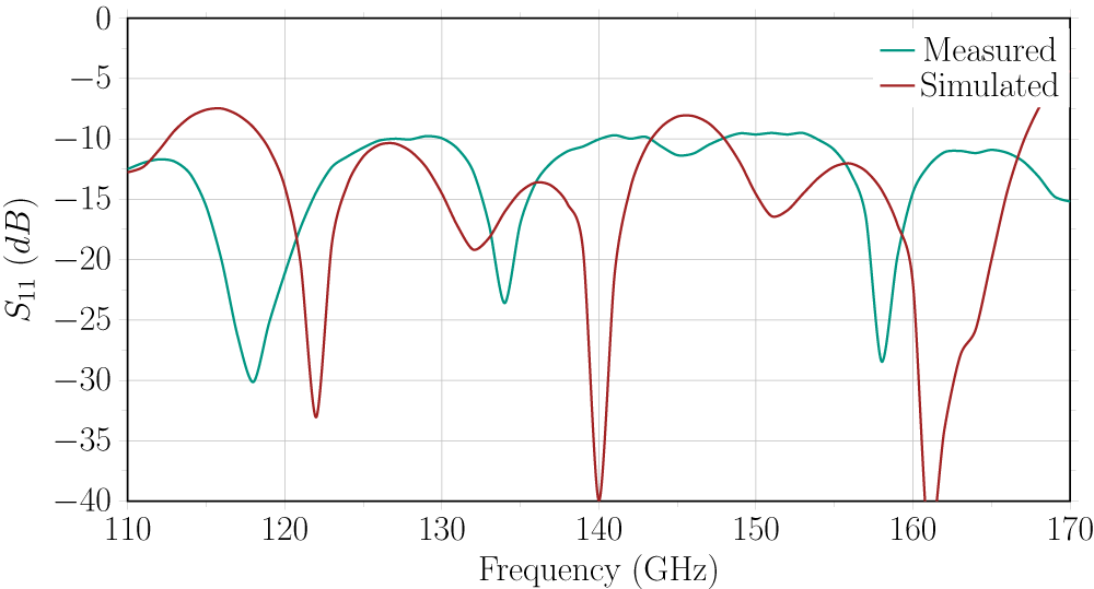
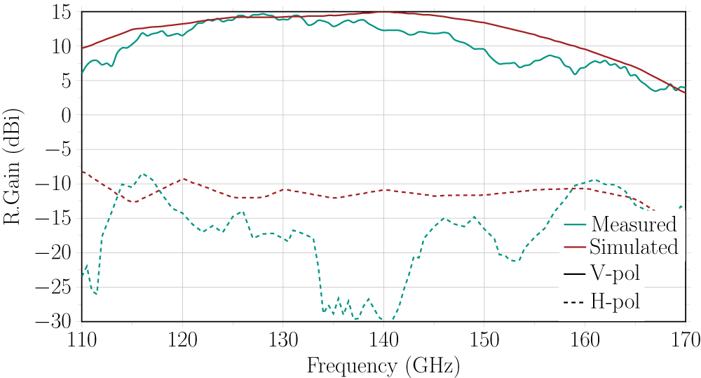
 $4\times4$ PIGRA array is presented in Figures 18 and 19. The
 $S_{11}$ curves shown in Figure 18 are below
 $-10\,\mathrm{dB}$ across almost the whole D-band frequency range. The measured broadside realized gain of the vertically polarized (V-pol.) component reaches a peak of
 $15\,\mathrm{dBi}$ in Figure 19 at
 $128\,\mathrm{GHz}$. The cross-polarized (H-pol.) component remains
 $20$–
 $40\,\mathrm{dB}$ below the co-polarized (V-pol.) component across the operating band. The measured radiation patterns at peak-gain frequency are in good agreement with the simulation (Figure 20). The main beam is directed towards broadside, with a measured front-to-back ratio of approximately
 $7$–
 $8\,\mathrm{dB}$. The small deviations between simulation and measurement are mainly attributed to the influence of the GSG probe. A slight asymmetry is observed in the transverse-plane radiation patterns (Figure 20(a) and (c)), primarily caused by the feed network and the probe influence. The influence of the assembly tolerances was also investigated. The measured positioning error of the glass radiator was below 130 µm, with angular misalignment below
 $4^\circ$ (Figure 21).
PIGRA radiation pattern at  $138\,\mathrm{GHz}$, transversal cut, V-pol.

 $|S_{11}|$ of the
 $4\times4$ PIGRA array.

Realized gain of the  $4\times4$ PIGRA array.

 $4\times4$ PIGRA array radiation pattern at
 $128\,\mathrm{GHz}$.

Figure 20 Long description
A polar line plot labeled, Transversal plane, V pol. A legend lists, Measured, Simulated and Sim. EP. The angular axis is marked in degrees from 0 degree to 360 degree. The radial axis label is dBi, with labeled rings at 15, 5, minus 5, minus 15, minus 25 and minus 35. The three curves form a main lobe near 0 degree close to the 15 ring. Additional lobes appear around about 60 degree, about 180 degree and about 300 degree. The Measured curve shows multiple small ripples between about 90 degree and 150 degree and between about 210 degree and 270 degree. The image B showing a polar line plot labeled, Longitudinal plane, V pol. A legend lists, Measured, Simulated and Sim. EP. The angular axis is marked in degrees from 0 degree to 360 degree. The radial axis label is dBi, with labeled rings at 15, 5, minus 5, minus 15, minus 25 and minus 35. The three curves show a dominant lobe near 0 degree close to the 15 ring. A deep notch appears near about 30 degree to 40 degree, reaching toward the minus 35 ring. A broad lobe appears near about 180 degree. Smaller lobes appear near about 300 degree and near about 90 degree to 120 degree. The Measured curve shows jagged variations near about 120 degree to 160 degree. The image C showing a polar line plot labeled, Transversal plane, H pol. A legend lists, Measured, Simulated and Sim. EP. The angular axis is marked in degrees from 0 degree to 360 degree. The radial axis label is dBi, with labeled rings at 15, 5, minus 5, minus 15, minus 25 and minus 35. The curves lie mostly between the minus 5 and minus 35 rings. The Measured curve has many narrow spikes between about 240 degree and 300 degree and also around about 180 degree. The Simulated and Sim. EP curves are smoother, with a broader bulge near about 90 degree and another near about 210 degree. The image D showing a polar line plot labeled, Longitudinal plane, H pol. A legend lists, Measured, Simulated and Sim. EP. The angular axis is marked in degrees from 0 degree to 360 degree. The radial axis label is dBi, with labeled rings at 15, 5, minus 5, minus 15, minus 25 and minus 35. The curves form a rounded multi lobe shape mostly between the minus 5 and minus 25 rings. A dip reaches toward the minus 35 ring near about 30 degree to 40 degree. The Measured curve shows a sharper inward dip near about 150 degree to 180 degree than the other two curves.
Radiator positioning error.

Conclusion
A new wideband glass-based antenna concept for D-band applications has been presented. To the best of the authors’ knowledge, this work demonstrates for the first time a wideband glass-based GoG antenna concept in the D-band, covering a wide frequency range from 110 to  $170\,\mathrm{GHz}$, with a peak realized gain of
 $5.8\,\mathrm{dBi}$ for the single radiator and
 $15\,\mathrm{dBi}$ for the
 $4\times4$ array implemented on a 76
 $\mu$m-thick CLTE substrate.
State-of-the-art of D-band DRAs as single element and in array configuration

Table 3 Long description
Columns list number of DRAs, DRA shape, material and permittivity, frequency in GHz, relative bandwidth percent, realized peak gain in dBi, and reference. Single rectangular alumina with permittivity 10 covers 123 to 137 GHz with 11 percent relative bandwidth and 2.7 dBi realized peak gain, reference 34. Two stacked rectangular alumina with permittivity 10 covers 123 to 137 GHz with 11 percent relative bandwidth and 4.7 dBi realized peak gain, reference 34. Single rectangular alumina with permittivity 9.8 covers 115 to 162 GHz with 34 percent relative bandwidth and 5 dBi realized peak gain, reference 36. Single pyramidal glass BF33 with permittivity 4.4 covers 110 to 170 GHz with 43 percent relative bandwidth and 5.8 dBi realized peak gain, reference, This work. Array 4 by 4 rectangular glass BF33 with permittivity 4.4 covers 135 to 146 GHz with 8 percent relative bandwidth and 13.2 dBi realized peak gain, reference 37. Array 4 by 4 pyramidal glass BF33 with permittivity 4.4 covers 118 to 168 GHz with 35 percent relative bandwidth and 15 dBi realized peak gain, reference, This work.
The proposed approach is compared with recently reported dielectric resonators operating in D-band (Table 3). This work, compared to the work done by [Reference Hou, Xiong, Goh, Hu, Hong and Madihian34, Reference Li, Disch, Haag, Visweswaran, Bhutani and Zwick36, Reference Bekker, Yin, Valenziano, Lootze, Schulz-Ruhtenberg, Zwick and Bhutani37], shows that the proposed pyramidal inverted glass resonator antenna achieves the widest bandwidth and the highest peak gain, both as a single radiator and in an array configuration. This is due to the multimode excitation in the operating D-band.
The glass resonator radiator was fabricated using LIDE technology, while the glass-based PCB was metallized using a two-step process consisting of PVD and electroplating. These fabrication processes are based on mature semiconductor-compatible technologies.
This work demonstrates, for the first time, a wideband glass-based D-band antenna integrated on a glass substrate metallized through PVD and electroplating processes. In particular, it validates the feasibility of 2.5D glass micromachining beyond  $100\,\mathrm{GHz}$. The presented results represent a significant advancement toward GoG AiP solutions for sub-THz applications, enabling potential applications in 6G communication systems, beyond-6G technologies, and radar sensing.
Funding statement
This work is supported financially by the Federal Ministry of Education and Research of Germany, through the projects ESSENCE (grant number 16KISK173) and X-TREME 6G (grant number 101192681).
Competing interests
None declared.

Mario Faliero received the M.Sc. degree in telecommunication engineering from the University of Siena, Siena, Italy. Following a career in industry where he held several engineering and management roles within the European telecommunication and automotive sectors, he joined the Karlsruhe Institute of Technology (KIT), Karlsruhe, Germany, where he is currently a research assistant. His research activities focus on analytical and applied electromagnetics, antenna theory, and antenna design, with specific interests in artificial electromagnetic structures, wideband impedance layered structures, and soft and hard boundary materials.

Thomas Zwick (Fellow, IEEE) received the Dipl.-Ing. (M.S.E.E.) and the Dr.-Ing. (Ph.D.E.E.) degrees from the University Karlsruhe (TH), Germany, in 1994 and 1999, respectively. From 1994 to 2001, he was a research assistant at the Institut für Hochfrequenztechnik und Elektronik (IHE) at the University Karlsruhe (TH), Germany. In February 2001, he joined IBM as a research staff member at the IBM T. J. Watson Research Center, Yorktown Heights, NY, USA. From October 2004 to September 2007, Thomas Zwick was with Siemens AG, Lindau, Germany. During this period, he managed the RF development team for automotive radars. In October 2007, he became a full professor at the Karlsruhe Institute of Technology (KIT), Germany. He is the director of the Institut für Hochfrequenztechnik und Elektronik (IHE) at the KIT.

Akanksha Bhutani received the M.Sc. and Ph.D. degrees in electrical engineering and information technology from the Karlsruhe Institute of Technology (KIT), Karlsruhe, Germany, in 2012 and 2019, respectively. Since 2019, she has been leading the Antennas and Packaging research group at the Institute of Radio Frequency Engineering and Electronics, KIT. Her research work focuses on THz antennas and packaging for radar and wireless communication systems.











 Open access

