Introduction
In microelectronic products and systems, solder joints (interconnects) have been extensively used to act as physical, mechanical, and electrical connections [Reference Kang and Sarkhel1]. Recently, there is an increasing trend to use Sn–Bi-based alloys as solders or as the important elements in Sn–Bi–X composition mixed solders to improve the microstructure and mechanical properties of solder joints [Reference Wang, Huang and Du2, Reference Huang, Zhou and Zhang3]. Sn–Bi-based alloys have salient features [Reference Hua, Mei and Glazer4, Reference Kotadia, Howes and Mannan5, Reference Mokhtari and Nishikawa6], such as lower melting temperature and lower coefficient of thermal expansion, in addition to the merits of lead-free and low cost. Moreover, owing to the relatively high processing temperature of mainstream lead-free solders (such as Sn–Ag–Cu and Sn–Ag-based solders) and increasing demand for multistep reflow soldering assemblies, in recent years there has been an increase in use of Sn–Bi-based solders in microelectronic packaging [Reference Kotadia, Howes and Mannan5, Reference Cheng, Huang and Pecht7]. In general, the eutectic alloys have features of low melting temperature and good liquidity; among binary Sn–Bi alloys, the eutectic Sn–Bi (i.e., Sn58Bi) alloy solder has become a popular choice. Further, it is worth noting that when the microelectronic products or devices are in service condition, the solder joints are subjected to the complicated loading of multiphysical fields, in which the electric current can induce the mass migration in the joints, i.e., electromigration, and it has become a critical reliability issue for electronic packaging. Owing to small dimensions of solder joints, usually at micro- and submicro-scale, the electric current density in the solder joints can reach a high level of 104 A/cm2 and even higher [Reference Tu8], which may lead to microvoid nucleation and propagation [Reference Yeh, Choi, Tu, Elenius and Balkan9], hillock formation [Reference Liu, Chih, Liao and Tu10], polarity effect of intermetallic compound (IMC) formation [Reference Gan and Tu11], phase segregation [Reference Yang and Shang12], and local melting [Reference Tsai, Lin, Tsai, Lai and Kao13]. For joints fabricated by reflow soldering using Sn58Bi solder on Cu substrate (or under bump metallization, UBM), i.e., Sn58Bi/Cu joints, the lower melting point may render the solder more susceptible to electromigration [Reference Yang and Shang12], then the electromigration reliability issue becomes more serious. Moreover, the migration of Bi atoms results in the formation of Bi monolayer segregated to the interface between Cu and Cu–Sn IMC, which can greatly reduce the reliability of solder interconnects caused by the decrease in the interface fracture resistance [Reference Liu and Shang14]. Many previous studies [Reference Chen, Chen and Lin15, Reference Chen and Huang16, Reference Xu, Guo, Wang, Xia, Lei, Shi and Li17] showed that the high-density electric current can promote the directional migration of Bi atoms and segregation of the Bi-rich phase, resulting in the inhomogeneous distribution of solder microstructure and even the separation of the Cu–Sn IMC and solder microstructures. In addition, the segregation of Bi atoms to the interface between Cu and IMC can induce the void formation [Reference Liu and Shang18, Reference Shang, Liu, Li and Shang19], while the Sn-rich phase layer and the Bi-rich phase layer formed at the cathode and anode sides, respectively, due to electromigration of Bi atoms may lead to the change in fracture position from the interface between the solder and IMC to the Bi-rich phase layer [Reference Liu and Shang20, Reference Gu and Chan21]. Furthermore, the effect of high-density electric current on the coarsening of microstructure of Sn58Bi solder is another reliability concern because the microstructure coarsening can lead to severe phase separation and consequently a significant decrease in the solder strength [Reference Zou, Zhang and Zhang22, Reference Zou, Zhang and Zhang23]. Although previous studies demonstrated that high-density electric current can promote the microstructure coarsening of Sn58Bi solder joint [Reference Gu and Chan21, Reference Chen and Chen24, Reference Chen, Huang, Liao and Liou25], the effect has only been studied qualitatively, some key issues need to be understood quantitatively and comprehensively, which include, for instance, the interaction between electromigration and segregation of the microstructures of Sn58Bi solder and the underlying mechanism, and the mutual influence of current density distribution and microstructure evolution.
When a high-density electric current flows through the Sn58Bi/Cu solder joint, the heat energy is generated due to Joule heating effect, which inevitably brings about thermal expansion and thermal mismatch of different materials, such as chips and substrates, and consequently leads to severe thermal stress in the packaged structure. Moreover, the Joule heating effect in the Bi-rich phase and the Sn-rich phase is different due to the difference in the resistivity of Bi-rich and Sn-rich phases, which definitely induces the thermal mismatch, at a microstructural level, between the Bi-rich phase and the Sn-rich phase. It has been shown that the external stress and high thermal stress induced by the thermal mismatch can significantly influence the microstructure evolution [Reference He, Xu and Guo26, Reference Zuo, Ma, Liu, Shu and Guo27]. In turn, the mechanical and physical response characteristics of the solder joint can also be greatly affected by the microstructure change through the underlying mechanisms of the migration of Bi atoms and segregation of the Bi-rich phase in Sn58Bi/Cu solder joints under electric current stressing, which have not been noticed and understood yet. Additionally, it should be indicated that the Bi-rich phase is very brittle in Sn58Bi solder, and cracking is more likely to initiate in the phase or at its interface, then the effect of stresses on initiation and propagation of cracks cannot be ignored, especially under the coupled loads of electric current stressing and thermal–mechanical stress.
However, the dynamic evolution of microstructure in Sn58Bi solder cannot be captured easily, there are only few studies [Reference Zuo, Ma, Liu, Shu and Guo27, Reference Ma, Zuo, Liu, Guo and Wang28] trying to describe the microstructure characteristics of Sn58Bi/Cu solder joints with considering the coupling effect of electric current stressing and elastic stress, despite a limited extent in understanding the combined effect as presented in the work. The computer simulation has shown the great potential for characterizing the microstructural evolution with high efficiency and low cost. In particular, the phase field method, which does not require explicit tracking of the constantly changing phase interfaces and can take into account the thermodynamic and physical properties of alloys, has been effectively used to investigate the dynamic evolution of the microstructure in Sn–Pb and Ag–Cu alloys [Reference Ubachs, Schreurs and Geers29, Reference Anders, Hesch and Weinberg30]. In our latest study [Reference Liang, Ke, Huang, Zhou and Zhang31], the microstructure evolution of the Sn58Bi solder in a line-type solder interconnect under the condition of isothermal aging and temperature gradient was effectively simulated and investigated by a developed phase field model. Heretofore, the coupling effect of electric current stressing and elastic stress on the microstructure evolution of the solder has not been considered in most of the existing phase field models; thus, it is highly necessary for us to characterize and understand the microstructure evolution of Sn58Bi/Cu solder joints because the electrical and mechanical properties of the solder joints are closely related to characteristics and dynamic evolution of the joints’ microstructure, especially when the degree of integration of microelectronic packages is continuously increasing and the dimension of solder joints is successively scaling down.
In this study, a two-dimensional phase field model is developed to investigate the microstructural evolution and predict the change in macroscopic physical properties of a flip chip Cu/Sn58Bi/Cu joint under the conditions of isothermal aging and the coupling effect of electric current stressing and elastic stress. The migration of Bi atoms and the segregation of the Bi-rich phase in the solder joint are dynamically simulated by incorporating the interaction effects among atom diffusion, electric field, and the elastic field caused by the electric current stressing as well as the thermal mismatch between chip and substrate materials. Furthermore, the effects of electromigration and segregation of the Bi-rich phase on the current density distribution and voltage of Sn58Bi solder have been investigated, and the interaction effect between the current density distribution and the microstructure characteristics is clarified. In addition, the redistribution of von Mises stress in the solder joint due to the microstructural evolution of Sn58Bi solder is studied deeply, and the effects of the electric current stressing on the coarsening kinetics of the Bi-rich phase in the Cu/Sn58Bi/Cu joint are discussed comprehensively.
Simulation results
Microstructural evolution of Sn58Bi solder during isothermal aging
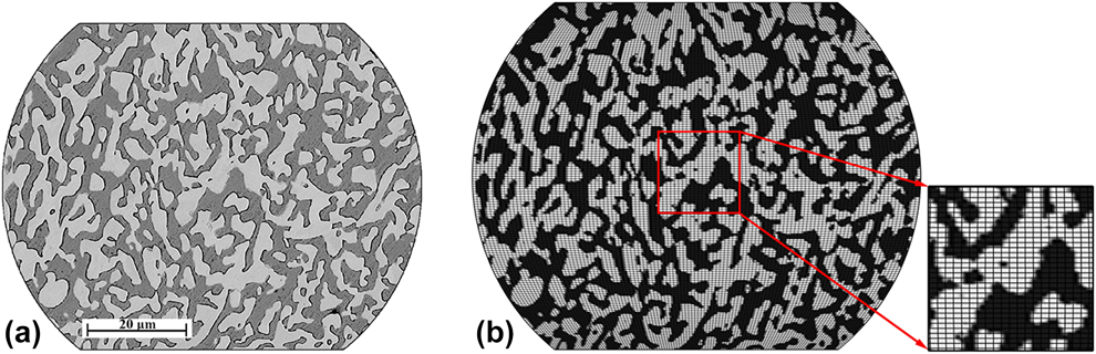
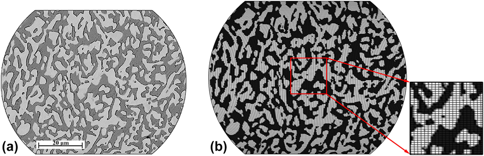
The microstructure of Sn58Bi solder after reflow process from our experimental study is shown in Fig. 1(a), in which the Sn-rich phase (dark areas) and the Bi-rich phase (bright areas) are mutually related. In the experiment, a reflow profile with peak temperature of 186 °C and duration of 70 s above the melting point of Sn58Bi solder (i.e., 139 °C) was used. Based on the experimental observation, i.e., scanning electron microscopy (SEM) image shown in Fig. 1(a), a finite element model is constructed, as shown in Fig. 1(b). The model is discretized by 17,854 quadrilateral elements, and the value distribution of concentration C in the two-dimensional domain is assigned on the basis of the RGB matrix of the image. Therefore, the bright regions with C = 1 shown in Fig. 1(b) correspond to the Bi-rich phase, while the dark regions with C = 0 correspond to the Sn-rich phase shown in Fig. 1(a). Moreover, the value of C in the interfacial layer between the Sn-rich phase and the Bi-rich phase is assumed to vary smoothly between 0 and 1.
Scanning electron microscopy image of microstructure of the as-reflowed Sn58Bi solder obtained from experimental study (a) and (b) the constructed microstructure finite element model based on (a).
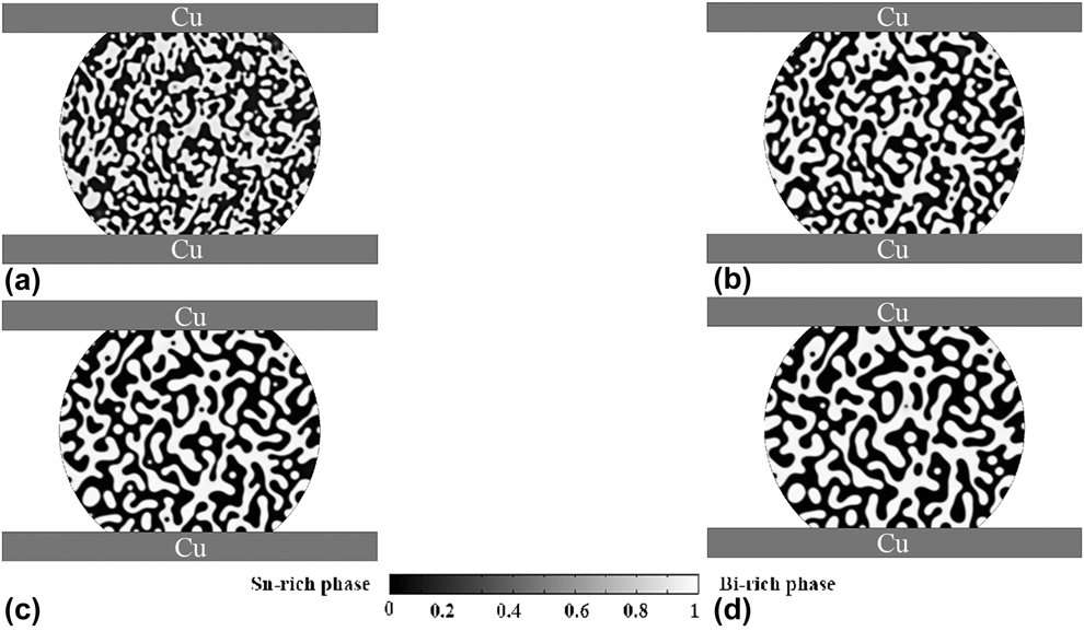
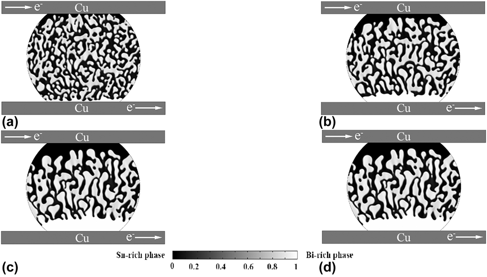
After setting the initial distribution of concentration C as discussed above, and taking no account of the driving forces related to electrical energy and elastic energy, then the microstructure evolution of Sn58Bi in the joint during isothermal aging can be investigated by using the phase field model described in the “Introduction” section. It should be pointed out that assigning the initial distribution of concentration C based on the experimental image can make simulation results be more reasonable and convincing. The simulation result of the morphological evolution of the microstructure of Sn58Bi solder in the joint for different times is presented in Fig. 2, where the distribution of concentration C in the solder domain is indicated by a white to black grayscale bar at the bottom. Clearly, the Bi-rich phase and the Sn-rich phase are separated in the solder matrix during the isothermal aging process. Meanwhile, the microstructure coarsening occurs obviously, in which the large-sized phase particles grow at the expense of the small-sized ones, as exhibited comparatively in Figs. 2(a) and 2(d). Comparing the present results with that reported in the latest study [Reference Liang, Ke, Huang, Zhou and Zhang31], the microstructure characteristics are somewhat different due to different simulation conditions, but significant coarsening of the microstructure can be found in both studies. It is worth indicating that the stark microstructure coarsening behavior of Sn58Bi solder was also observed more often in experimental studies [Reference Jin and McCormack32, Reference Chen, Ho, Lin, Luo and Kao33, Reference Miao and Duh34], which may lead to performance degradation of the solder joints.
Morphological evolution of the microstructure of Sn58Bi solder in a flip chip Cu/Sn58Bi/Cu joint during isothermal aging for different nondimensional times: (a) τ = 10, (b) τ = 50, (c) τ = 150, and (d) τ = 300.

Microstructural evolution of Sn58Bi solder under electric current stressing and elastic field
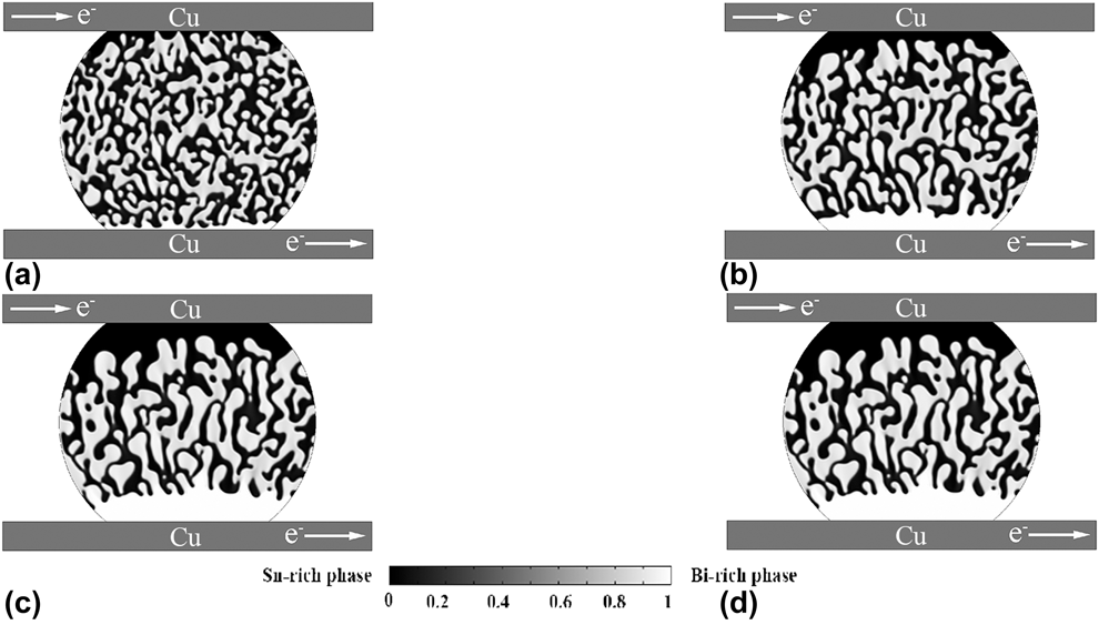
When electric current with a current density of 1.5 × 10⁸ A/m2 is applied to the flip chip Cu/Sn58Bi/Cu joint, the electric current stressing, together with the driving force induced by chemical gradient, can drive the directional migration of atoms. Meantime, during the operation process of electronic products or devices, the temperature of solder joints increases due to the Joule heating effect. Assuming that the thermal mismatch of materials between the chip and substrate leads to the upper Cu pad having a displacement relative to the lower Cu pad along the direction of the bottom end of the simulation domain. Generally, the shear displacement closely depends on the solder joint size, thermal loading mode, and the distribution of solder joints in microelectronics. In the widely used flip chip Sn–Pb solder joints, the shear strain of solder bumps can vary from 0.1 to 1.0% [Reference Gu and Nakamura35]. With taking into account the lower fatigue life of SnBi solder than that of SnPb solder, i.e., the latter is about three times of the former [Reference Mei and Morris36], thus, it is reasonable to assume a relatively small shear strain applied to the SnBi solder joint in this study, and the shear displacement is set as s = 0.02 μm, then the shear strain of the solder bump is about 0.033%. Considering that there is a coupling effect of electric current stressing and elastic stress induced by the above thermal mismatch, then the microstructural evolution of Sn58Bi solder in the joint, with the initial microstructure corresponding to Fig. 1, is simulated, and the results are exhibited in Fig. 3. Obviously, there is a redistribution of both Bi-rich and Sn-rich phases. Bi-rich phase particles migrate along the direction of electron flow, and the thickness of the Bi-rich phase layer formed at the anode side increases with the nondimensional time, which was also observed in previous experimental studies [Reference Chen, Huang, Liao and Liou25, Reference He, Zhao, Guo and Xu37]. Meanwhile, Sn atoms migrate in the opposite direction to that of Bi atoms migration (i.e., electron flow direction) and a segregated layer of the Sn-rich phase forms at the cathode side. The above simulation results are consistent with the results of experimental characterization [Reference Yang and Shang12, Reference Chen and Huang16, Reference Xu, He and Guo38]. When τ = 100, it can be seen that Sn-rich and Bi-rich phases are severely separated, and the direct interconnection between Sn58Bi solder and Cu pads is also separated due to the formation of Bi-rich and Sn-rich phase layers, which results in severe microstructural inhomogeneity and deteriorates the structural integrity of the solder joint. Notably, Bi-rich phase particles shown in Figs. 3(c) and 3(d) align almost parallel to the direction of electron flow, which are very different from the initial microstructure at current-free state shown in Fig. 2. It is worth mentioning that the similar phenomenon was also observed in SnPb solder stripes in an experimental study [Reference Chou, Chen, Liang and Chen39], which showed that Pb-rich grains align parallel to the electron flow direction, as a consequence of the high-density current stressing. In addition, a detailed comparison of the microstructure characteristics between Figs. 3(d) and 2(c), both for τ = 150, indicates that obvious coarsening of microstructure has occurred. This means the current stressing has significant influence not only on segregation of the Bi-rich phase and the Sn-rich phase but also on microstructure coarsening of Sn58Bi solder.
Morphological evolution of the microstructure of Sn58Bi solder in a flip chip Cu/Sn58Bi/Cu joint under electric current stressing for different nondimensional times: (a) τ = 10, (b) τ = 50, (c) τ = 100, and (d) τ = 150.
It is noteworthy that the effect of elastic field induced by the thermal mismatch on microstructural evolution of the joint is not obvious in the present study. The reason behind this is probably that the stress concentration is mainly located at the four vertex positions of the solder near the interface between the pad and Sn58Bi solder, and the magnitude of the average stress is so small that the influence is slight and nearly neglectable. Actually, this phenomenon had also been seen in studies of coarsening process of SnPb solders, in which a tensile stress with level of 5–10 GPa only leads to a slight acceleration of microstructure coarsening in SnPb solder [Reference Dreyer and Müller40, Reference Li and Müller41], and the stress is much higher than the yield strength of the solder (∼43.0 MPa) and may have caused fracture or other types of failure of solder joints. Considering the fact that the thermal stress induced by the thermal mismatch in the present study is only about 4 MPa (much lower than 5 GPa), the simulation results that have not shown the visible effect of elastic stress field on microstructural evolution are reasonable.
Discussion
Correlation between the current density distribution and the microstructure characteristics
The above simulation results have shown that the current stressing can induce the microstructure segregation and obvious coarsening of the microstructure, as shown in Figs. 2 and 3. Due to the differences in electrical conductivity and Young’s modulus between Sn-rich and Bi-rich phases, the electric current carrying capacity and the mechanical response characteristics of solder joints will be greatly affected by the microstructural evolution in the Sn58Bi/Cu solder joints, which can lead to the electrical resistance change in the solder joint and the crack initiation in embrittlement along the solder/Cu interface, as observed in the previous studies [Reference Sun, Xu, Guo, Xia, Lei, Shi, Li and Wang42, Reference Zhang, Zou and Zhang43]. Moreover, the segregation of the Bi-rich phase near the Cu3Sn/Cu interface of the Sn58Bi/Cu solder joints can induce the void formation near the Cu side [Reference Shang, Liu, Li and Shang19]. In particular, it is worth pointing out that the separation of the Bi-rich phase and the Sn-rich phase shown in Fig. 3(d) can result in composition deviation in partial solder regions away from the eutectic component of Sn–Bi alloys, thus melting characteristics of the solder may change. For instance, the solder’s melting point temperature (solidus temperature) remains unchanged (139 °C), while the liquidus temperature is increased, which may be higher than the eutectic melting temperature of Sn58Bi solder (139 °C). In the case of complete separation of the two phases, i.e., the “solder” consists of two separated Sn-rich and Bi-rich phases, the melting temperature of the “solder” joint is actually the melting point temperature of Sn (232 °C), rather than 139 °C. It is especially worth pointing out that for SnBi-based alloys (including Sn58Bi) used as fuse wire in electronic and electrical devices/systems for overcurrent protection, the increase in melting temperature of SnBi alloys due to severe phase separation can postpone the occurrence of melting and thus delay interruption of the current, and this will pose a serious challenge to safety and reliability of the devices and systems using SnBi alloys.
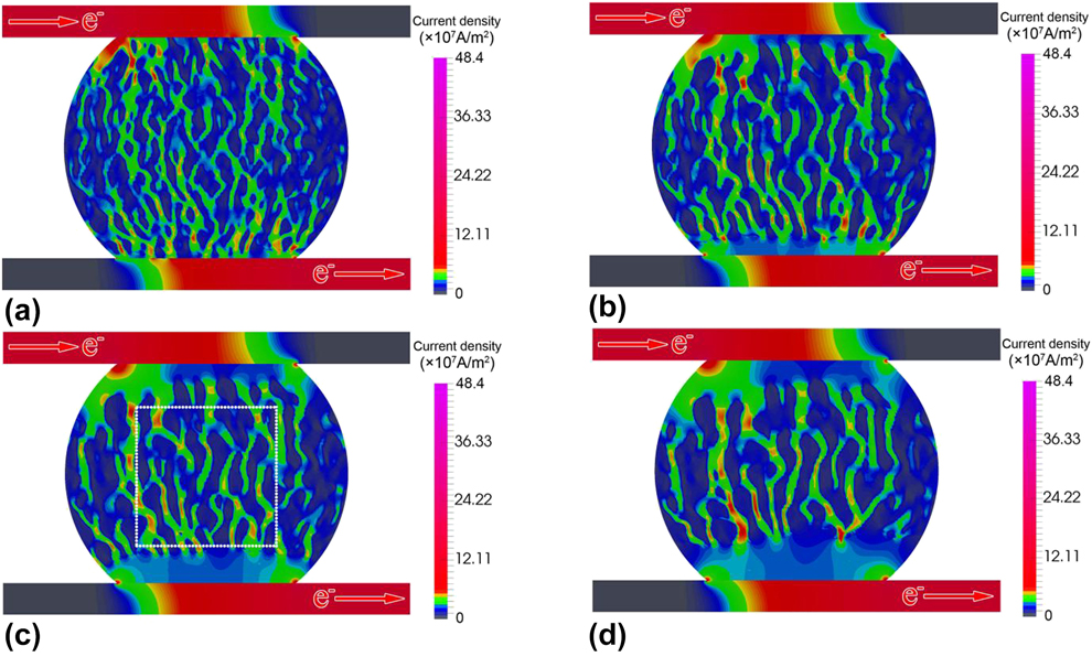
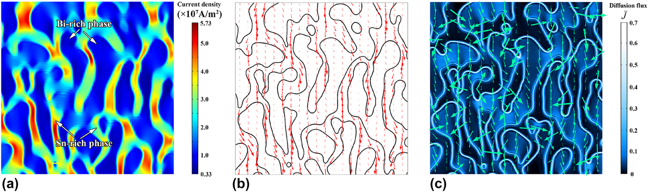
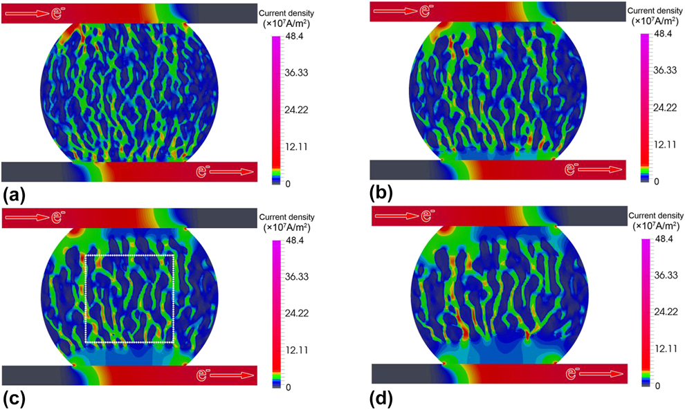
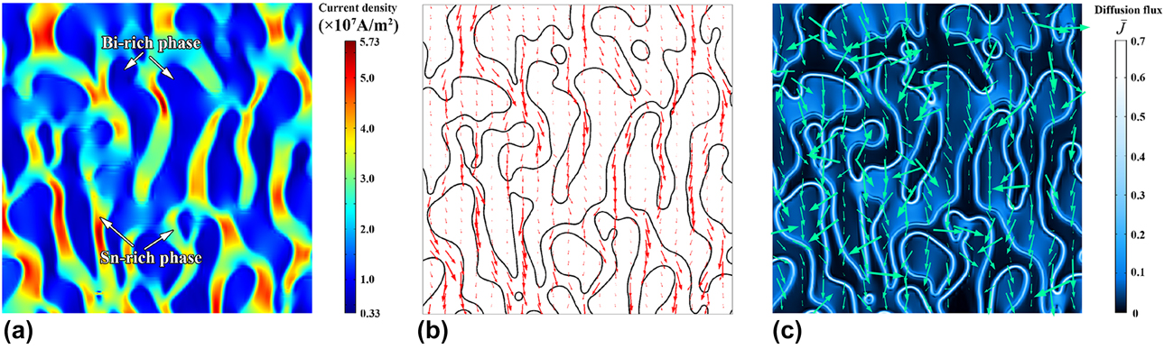
As demonstrated above, electric current stressing has significant influence on segregation and coarsening of the microstructure, and vice versa; the microstructural evolution and phase segregation also have obvious effect on distribution of current density. Figure 4 shows the current density distribution in the solder joint under electric current stressing with a current density of 1.5 × 10⁸ A/m2. Clearly, the current density distribution in the solder directly relates to microstructure characteristics of Sn58Bi solder shown in Fig. 3, which shows that the Sn-rich phase carries more current and the current density in the Sn-rich phase is higher than that in the Bi-rich phase. Figure 5(a) shows the current density distribution in a localized region of Sn58Bi solder, marked by the white dotted line box in Fig. 4(c). Apparently, the current density in the Sn-rich phase is higher than that in the Bi-rich phase. This is because of higher electrical conductivity of the Sn-rich phase than the Bi-rich phase, and more electron carriers drift with higher velocity in the Sn-rich phase. Figure 5(b) presents the distribution of electron flow vectors, where the thickness of red arrows is proportional to the corresponding electric current magnitude shown in Fig. 5(a), and it is seen clearly that the current mainly passes through the Sn-rich phase and bypasses the Bi-rich phase. Then, according to the relationship between electric current density j e and electric potential U, which can be written as j e = −k(C)∇U, the inhomogeneous distribution of j e can affect the distribution of U. Note that the diffusion flux of Bi atoms can be defined as follows:
 $$\bar{J} = - \bar{M}\left( C \right)\nabla \left( {\bar{\mu } - \bar{U}} \right)\quad ,$$
and the distribution of  $\bar{J}$ in the microdomain indicated by the dotted-line box in Fig. 4(c) is shown in Fig. 5(c). Definitely, the diffusion flux in the Bi-rich phase is higher than that in the Sn-rich phase, and the diffusion flux near the interfaces between Bi-rich and Sn-rich phases is large. Besides, the diffusion fluxes mainly flow toward the anode side due to electric current stressing, and the flow direction is somewhat related to the interface curvature. In addition, it should be understandable that the aggregating electric current in the Sn-rich phase can affect the distribution of Joule heat in the domain shown in Fig. 5(a), then the temperature distribution is uneven, which may lead to the local melting or recrystallization of the solder in Sn58Bi/Cu solder joints under electric current stressing [Reference Xu, He and Guo38], and a similar phenomenon had been observed in eutectic SnPb flip chip solder joints [Reference Choi, Yeh and Tu44, Reference Ouyang, Tu and Lai45]. For the Bi-rich phase layer formed at the anode side, more Joule heat is generated in the solder part near the lower Cu pad, as shown in Fig. 4(d), which is caused by higher resistivity of the Bi-rich phase. Consequently, the temperature of Sn58Bi solder is increased because the Joule heating effect near the anode side is stronger than that near the cathode side where a Sn monolayer has formed, which can further promote Bi atoms to migrate to the anode side of the solder joint.
Current density distribution in a flip chip Cu/Sn58Bi/Cu joint under electric current stressing for different nondimensional times: (a) τ = 10, (b) τ = 50, (c) τ = 100, and (d) τ = 150.
Distributions of (a) current density and (b) electron flow vectors as well as (c) diffusion flux in a localized region marked by the dotted line box in Fig. 4(c).
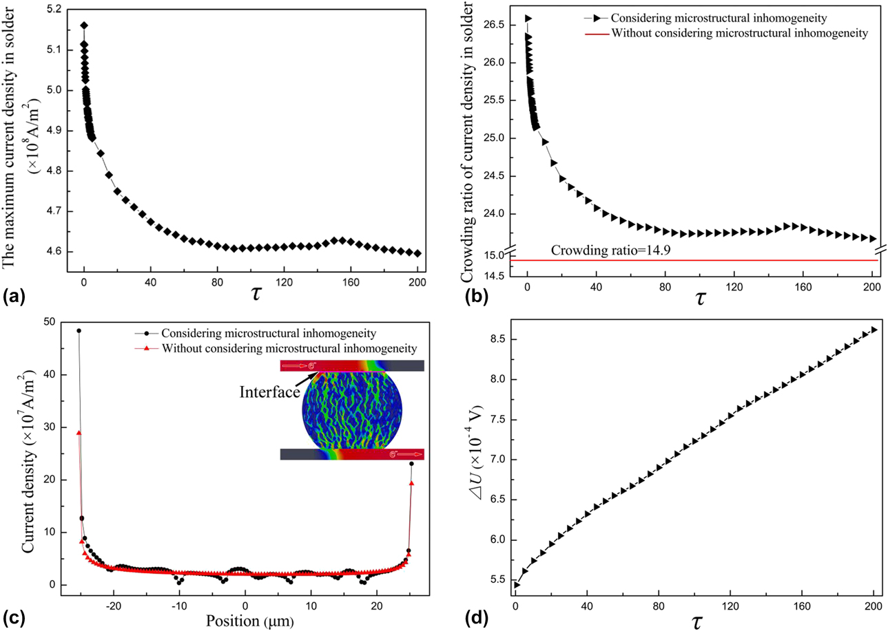
To further clarify the effect of microstructure evolution of Sn58Bi solder on the electric current density distribution, the maximum current density and the current crowding ratio of the maximum current density to the average current density in solder as a function of the nondimensional time (τ) are calculated, and the results are shown in Figs. 6(a) and 6(b). Clearly, at initial stage the maximum current density decreases sharply and then fluctuates slightly with time, as depicted in Fig. 6(a). Notably, the slight change in the maximum current density is due to increase in electromigration resistance of the Bi-rich phase, which is caused by migration of Bi atoms to the anode side of the solder joint. Similarly, the current crowding ratio first shows a rapid decrease and then changes slowly with time when considering the effect of inhomogeneous microstructure, as presented in Fig. 6(b). In addition, the current crowding ratio is calculated as 14.9 in the Cu/Sn58Bi/Cu joint without considering the inhomogeneous microstructure of the solder, which is much smaller than the current crowding ratio corresponding to the solder joint with considering the inhomogeneous microstructure. This indicates that the current crowding effect can be more obvious in the flip chip solder joint due to the inhomogeneous microstructure of Sn58Bi solder, which may promote the formation and growth of voids and hillocks as observed in the experimental studies [Reference Gu and Chan21, Reference Xu, He and Guo38, Reference Gu and Chan46, Reference Yue, Qin, Zhou, Ma and Zhang47]. Yet, despite the decrease of current crowding ratio with time, the possibility of reliability degeneration of Cu/Sn58Bi/Cu joints may not be reduced because the phase segregation can usually decrease the reliability along the interface between Sn-rich and Bi-rich phases and the solder/Cu interface.
(a) Changes of the maximum current density and (b) the crowding ratio of current density in Sn58Bi solder as a function of the nondimensional time. (c) Current density distribution along the interface between the Cu pad and the solder of the joint with the microstructural inhomogeneity corresponding to Fig. 3(a) for τ = 10 (the position 0 locates at the center of the interface). (d) Change of the voltage across the flip chip Cu/Sn58Bi/Cu joint as a function of the nondimensional time τ.
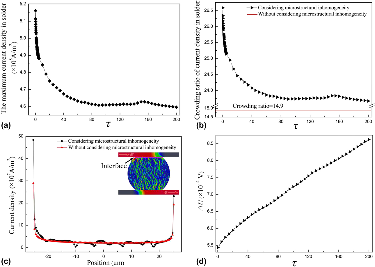
The current density distribution in Sn58Bi solder along the interface between the upper Cu pad and the solder is obtained, as shown in Fig. 6(c). Obviously, the current density distributes unevenly along the interface, which is caused by the combined effect of both the geometrical inhomogeneity of the flip chip solder joint at the macroscale and the microstructural inhomogeneity of Sn-rich and Bi-rich phases at the microscale. In particular for the microstructural inhomogeneity, it induces the localized nonuniform distribution of electric current density in Sn-rich and Bi-rich phases due to the big difference in electrical resistivity between Sn and Bi (i.e., 1.15 × 10⁻⁷ and 1.15 × 10⁻⁶ Ω m, respectively). Remarkably, the current density is highest at the entrance corner of electron flow from the Cu pad to the solder, which is due to the severe current crowding effect near the corner of the solder joint. It is clearly seen in Fig. 6(c) that the current densities at the corners of the Cu/Sn58Bi/Cu joint with considering the microstructural inhomogeneity are higher than those of the Cu/Sn58Bi/Cu joint without considering the microstructural inhomogeneity. In general, the high density current at the corner of flip chip solder joints can lead to the formation of voids and promote their propagation at the cathode side [Reference Yamanaka, Tsukada and Suganuma48, Reference Jen, Liu and Lai49, Reference Chang, Cheng, Xu, Helfen, Tian, Di Michiel, Chen, Tu and Baumbach50], and even cause open circuit failure of the solder joints. Moreover, the temperature rise induced by current crowding and Joule heating can drive the atoms to migrate rapidly, which may further promote the void formation and exacerbate microstructural inhomogeneity at the corners of solder joints.
The above results and analyses demonstrate clearly that the microstructure evolution of Sn58Bi solder has significant influence on the current density distribution of the joint. Accordingly, the voltage (∆U) change in the joint is also dependent on microstructure evolution, as shown in Fig. 6(d). Apparently, the electromigration and segregation of the Bi-rich phase result in rapid increase in voltage, for instance, the voltage has increased by 55% when τ = 200. Furthermore, the resistance R of the solder joint can be derived by the following equation:
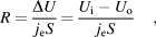 $$R = {{\Delta U} \over {{j_{\rm{e}}}S}} = {{{U_{\rm{i}}} - {U_{\rm{o}}}} \over {{j_{\rm{e}}}S}}\quad ,$$
where S is the cross-section area of the entrance of the electron flow and U i and U o denote the electric potential at current input side and current output side, respectively. Because both S and j e (i.e., electric current density) are constant, the resistance change can be reflected by the voltage variation. Obviously, the microstructure segregation and the Bi-rich phase layer formed at the anode side can lead to an increase in resistance of the flip chip Cu/Sn58Bi/Cu joint, which is similar to the observation and demonstration presented in the previous experimental studies [Reference Sun, Xu, Guo, Xia, Lei, Shi, Li and Wang42, Reference Guo, Xu, Sun, Xia, Lei, Shi and Li51]. Undoubtedly, the increased resistance will produce more Joule heat, which is more likely to accelerate the failure of solder joints.
Correlation between the elastic stress distribution and the microstructure characteristics
In the present simulation, the effect of elastic stress on the microstructure evolution is not obvious. This can be explained by much lower elastic strain energy density than the chemical energy density in the solder matrix. The high elastic strain energy density occurs at the four corners of the joint due to the geometrical inhomogeneity of the flip chip solder joint. In Sn58Bi solder, the maximum elastic strain energy density is 2.46 × 10⁵ J/m3, and the average elastic energy density is about 2.68 × 10² J/m3. It is worth mentioning that the chemical energy density is usually in the order of magnitude of 109 J/m3 [Reference Anders, Hesch and Weinberg30, Reference Ohtani and Ishida52, Reference Park and Arróyave53], which is much higher than the elastic strain energy density of Sn58Bi solder. This means that the stress induced by thermal mismatch between chips and substrates has no obvious influence on the microstructure evolution in the solder of the flip chip Cu/Sn58Bi/Cu joint under electric current stressing.
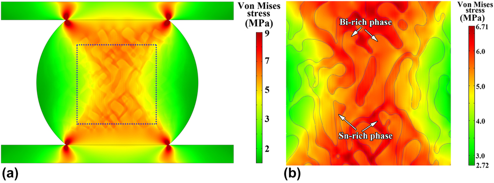
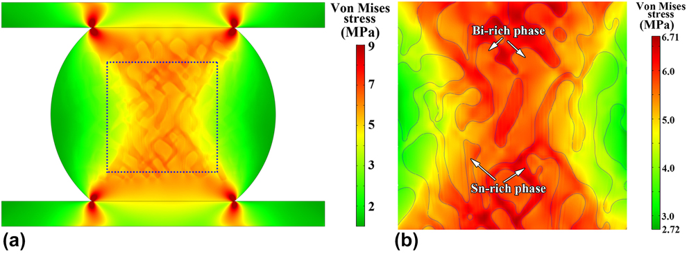
Furthermore, it is understandable that the evolution and segregation of the Bi-rich phase in the solder can affect the stress distribution in the flip chip Cu/Sn58Bi/Cu joint because Sn-rich and Bi-rich phases have different elastic modulus values, which are 41.0 and 31.9 GPa, respectively. Figure 7 exhibits the inhomogeneous distribution of von Mises stress in the solder joint and in two different phases (i.e., Sn-rich and Bi-rich phases). Evidently, the stress concentration occurs at the four corners of the solder joint, as shown in Fig. 7(a), and the stress is higher in the Sn-rich phase than in the Bi-rich phase, as presented in Fig. 7(b), which is resulted from the lower elastic modulus of the Bi-rich phase compared with the Sn-rich phase. It should be indicated that usually the Bi-rich phase in Sn58Bi solder is very brittle [Reference Felton, Raeder and Knorr54, Reference Raeder, Felton, Tanzi and Knorr55, Reference Mostofizadeh, Pippola and Frisk56], while the Sn-rich phase is relatively soft; thus, when an Sn58Bi solder joint is subjected to high stress, cracks are more likely to initiate and propagate at the interface between Bi-rich and Sn-rich phases.
Distribution of von Mises stress in (a) the flip chip Cu/Sn58Bi/Cu joint with the microstructure corresponding to Fig. 3(c), and (b) Sn58Bi solder region marked by the dotted line box in (a).
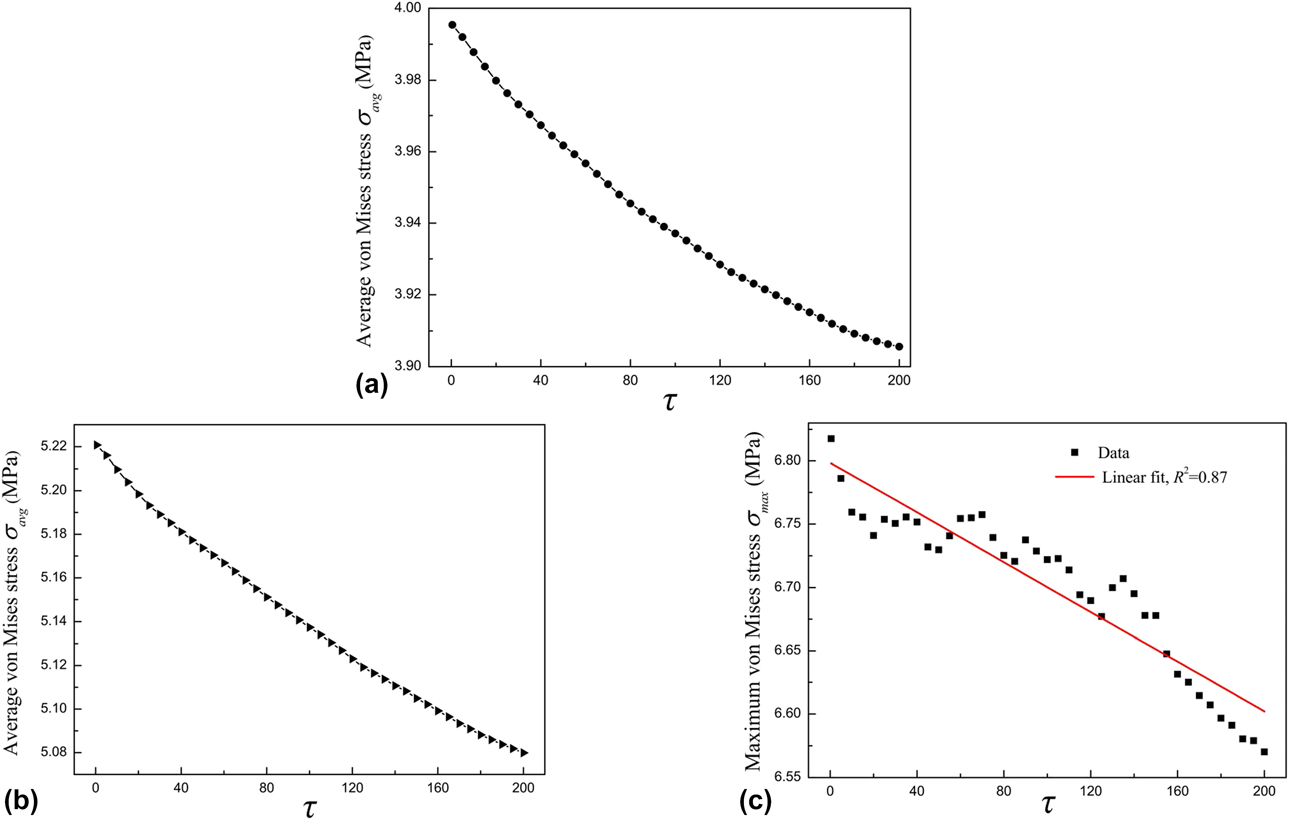
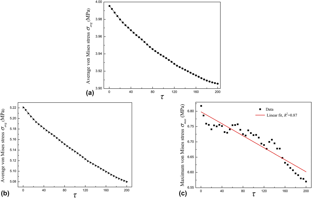
To depict quantitatively the variation of stress distribution affected by the directional migration and evolution of Sn-rich and Bi-rich phases in the solder, Fig. 8(a) presents the average von Mises stress in Sn58Bi solder as a function of the nondimensional time τ under electric current stressing. Apparently, the average stress decreases with the migration of the Bi-rich phase to the anode side. This is readily understandable in the way that migration and segregation of the Bi-rich phase can lead to decrease of the equivalent elastic modulus of Sn58Bi solder. To verify this point, Bi-rich and Sn-rich phases can be idealized as two springs with Young’s modulus E 1 and E 2, respectively, then Sn58Bi solder can be taken as a “spring model” consisted of the above two types of springs. The migration of Bi-rich and Sn-rich phases and their distribution along the electron flow direction can result in decrease in the equivalent elastic modulus, and the equivalent elastic modulus is E 1E 2/(E 1 + E 2) when the microstructure of Sn58Bi solder is completely separated into a Bi-rich phase layer and a Sn-rich phase layer. Clearly, the equivalent elastic modulus E 1E 2/(E 1 + E 2) is lower than either E 1 or E 2; thus, the average stress decreases. For the local region of the solder marked by the dotted line box in Fig. 7(a), both the average and maximum von Mises stresses also decrease with the time, as shown in Figs. 8(b) and 8(c). However, it should be pointed out that the coarsening of Sn-rich and Bi-rich phases can lead to the decrease in tensile strength of Sn58Bi solder [Reference Zou, Zhang and Zhang22, Reference Zou, Zhang and Zhang23]; therefore, the decrease in the von Mises stress due to migration and segregation of the Bi-rich phase does not mean the likelihood of failure of the solder joint is decreased, while implying that the load-bearing capacity of Sn58Bi solder is reduced because of the decrease in equivalent elastic modulus of the solder. Moreover, segregation of the Bi-rich phase and the formation of the Bi-rich phase layer at the anode side are most likely to initiate the interfacial crack, which had been frequently observed in previous studies [Reference Gu and Chan21, Reference Zuo, Ma, Liu, Shu and Guo27].
(a) The average von Mises stress in Sn58Bi solder as a function of the nondimensional time τ under electric current stressing, and changes of the (b) average and (c) maximum von Mises stresses in the partial solder region marked by the dotted line box in Fig. 7(a).
Effects of electric current stressing on coarsening of the Bi-rich phase
Based on the above results and analyses, it is evident that the coarsening of Sn58Bi solder is dependent on time. To depict the kinetics of the coarsening process of the Bi-rich phase, we can characterize the variation in the mean equivalent radius  $\bar{r}$ of Bi-rich phase particles, which is determined by the following equation:
 $$\bar{r} = \sqrt {{{\sum\limits_{i = 1}^N {{A_i}} } \over {\pi N}}} \quad ,$$
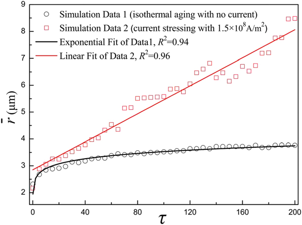
where A i is the area of each particle and N is the total number of Bi-rich phase particles, which are obtained by measurements using the Image-Pro Plus software, Media Cybernetics Inc., Maryland. Figure 9 shows the variation in the mean equivalent radius  $\bar{r}$ of Bi-rich phase particles versus the nondimensional time τ in Sn58Bi solder subjected to isothermal aging and electric current stressing, respectively. Clearly,
 $\bar{r}$ increases with time under both conditions, and the phase coarsening rate is higher under electric current stressing than under isothermal aging. The results of regression analysis manifest that there is an approximate linear relationship between
 $\bar{r}$ and τ under electric current stressing, while
 $\bar{r}$ is shown to be an exponential function of τ during the isothermal aging. Apparently, the coarsening of the Bi-rich phase is promoted by electric current stressing to proceed with a higher rate, and this phenomenon was also noticed in previous studies [Reference Gu and Chan21, Reference Chen and Chen24, Reference Chen, Huang, Liao and Liou25]. In particular, a recent experimental study [Reference Wang, Liu, Li and Wu57] reported that the higher density electric current induces faster grain growth of the Bi-rich phase, accordingly the diffusion mechanism of the Bi-rich phase is directly affected by the applied electric current. Moreover, it is worth mentioning that the similar phenomenon was observed in microstructure evolution of flip chip joint using eutectic Sn–Pb solder under current density [Reference Ye, Basaran and Hopkins58], which demonstrated that the higher density current leads to faster grain coarsening. In addition, it should be indicated that the Joule heating can be enhanced by electric current stressing, which may further lead to increase in temperature and then accelerate migration of atoms and finally cause faster coarsening of Sn58Bi solder. Similar results had been reported in previous studies about phase coarsening in Sn37Pb and Sn3.5Ag0.5Cu solder joints under current stressing [Reference Wu, Alam, Chan and Zhong59, Reference Wu, Zhong, Chan and Alam60]. Actually, the accelerated coarsening of the microstructure in the solder joints under temperature gradient was also observed [Reference Liang, Ke, Huang, Zhou and Zhang31], and there is a linear relationship between
 $\bar{r}$ and τ, meaning that electric current stressing has similar effect on the microstructure coarsening to temperature gradient.
Comparison of variation in the mean equivalent radius  $\bar{r}$ of Bi-rich phase particles versus the nondimensional time τ in Sn58Bi solder between isothermal aging and electric current stressing.
Conclusions
In this study, a phase field model is developed to simulate and characterize the microstructural evolution and the change in macroscopic physical properties of the flip chip Cu/Sn58Bi/Cu joint under conditions of isothermal aging and the coupled loads of electric current stressing and elastic stress. The following conclusions can be drawn:
(1) Under the coupled loads of electric current stressing and elastic stress, Bi atoms in Sn58Bi solder migrate along the electron flow direction, resulting in severe segregation of Bi-rich and Sn-rich phases in terms of formation of a Bi-rich phase layer on the anode side and a Sn-rich phase layer on the cathode side of the solder joint.
(2) There is an inhomogeneous current density distribution in Sn58Bi solder in microstructural level. The electric current density is higher in the Sn-rich phase than in the Bi-rich phase, and there is a tendency for electric current to transfer through the Sn-rich phase and detour the Bi-rich phase. The resistance of the solder joint increases and the average electric current density in Sn58Bi solder decreases with electromigration and segregation of the Bi-rich phase.
(3) Microstructural heterogeneity of Sn58Bi solder aggravates the current crowding effect near the entrance corner of electron flow from the Cu pad to the solder. The current crowding ratio in the solder matrix decreases rapidly at first and then fluctuates slightly with time, which is caused by migration behavior of Bi atoms to the anode side of the joint.
(4) Inhomogeneous microstructure of Sn58Bi solder leads to nonuniform von Mises stress distribution at the microstructural scale; the stress is higher in the Sn-rich phase than in the Bi-rich phase. The average von Mises stress in the solder joint decreases with time, which is induced by redistribution of Bi-rich and Sn-rich phases under the coupling effect of electric current stressing and elastic stress.
(5) The Bi-rich phase exhibits much faster coarsening rate under the coupled loads of electric current stressing and elastic stress than under isothermal aging. The coarsening kinetics can be described by an approximate linear relationship between the mean equivalent radius of the Bi-rich phase and the nondimensional time, showing similarity with microstructure coarsening characteristics under high temperature gradient.
Modeling methodology
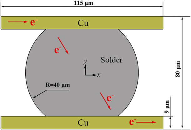
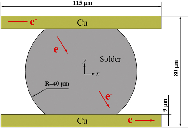
A phase field model is developed and then used to investigate the microstructural evolution and predict the change in macroscopic physical properties of a flip chip Cu/Sn58Bi/Cu joint under the conditions of isothermal aging and the coupling effect of electric current stressing and elastic stress. Figure 10 shows the geometrical model of a flip chip Cu/Sn58Bi/Cu joint, which consists of Sn58Bi solder and upper and lower Cu pads (substrates). The electron flow goes from the upper Cu pad to the lower Cu pad. When the electronic components are in service, a relative displacement between the upper and lower Cu pads can be established due to the thermal mismatch between chips and substrates. We assume the bottom boundary of the lower Cu pad is fixed, while the top boundary of the upper Cu pad is sheared by a horizontal displacement. It is known that the microstructure of Sn58Bi solder is usually composed of Sn-rich and Bi-rich phases [Reference Tu8], and IMC is formed between the Cu pad and the solder. For simplicity, in the simulation the IMC in the solder joint is ignored, a parameter C is introduced to represent the volume fraction of the Bi-rich phase in Sn58Bi solder, and C transits from 0 inside the Sn-rich phase to 1 inside the Bi-rich phase and varies smoothly across the interfacial layer. Then, the volume concentration distribution reflecting the microstructure characteristics of the solder can be described by the spatial and time-dependent variable C(x, y, t). The microstructural evolution in Cu pads is not taken into account in the present study.
Illustration of the geometrical model of a flip chip solder joint.
The free energy of the solder system (i.e., the gray region in Fig. 10) can be given by referring to a general expression for an inhomogeneous microstructure system [Reference Chen61]:
 $$F\left( {C,\varepsilon } \right) = \int_V {\left\{ {f\left( C \right) + {1 \over 2}{\varepsilon ^2}{{\left| {\nabla C} \right|}^2} + {E_{{\rm{el}}}}} \right\}} {\rm{d}}V\quad ,$$
where f(C) is the chemical free energy density of the system, the term  $\left( {{1 / 2}} \right){\varepsilon ^2}{\left| {\nabla C} \right|^2}$ accounts for the surface energy and ε is a material constant, and E el = 1/2σε is the elastic energy density, in which σ is the stress tensor and ε is the strain tensor. For a two-phase (i.e., Sn-rich and Bi-rich phases) solder system, the chemical free energy density of the system can be written as follows:
 $$f\left( C \right) = W{C^2}{\left( {1 - C} \right)^2}\quad ,$$
where W is a positive constant that characterizes the height of the double well.
When an electric current flows through the solder joint, the electric potential U is governed by:
 $$\nabla \cdot \left( {k\left( C \right)\nabla U} \right) = 0\quad .$$
When the above equation is applied in the solder region, the electrical conductivity function k(C) is assumed to be a linear combination of the electrical conductivities of the Sn-rich phase and the Bi-rich phase weighted by the concentration C, i.e.,
 $$k\left( C \right) = {k_{{\rm{Sn}}}}\left( {1 - C} \right) + {k_{{\rm{Bi}}}}C\quad .$$
The electrical conductivity function k(C) is considered equal to the electrical conductivity of copper, k Cu, when the equation is applied in Cu pads.
Considering the shear displacement of the upper Cu pad, the elastic stress field can be computed by the following equation:
 $$\nabla \cdot \sigma = 0\quad .$$
When the above equation is applied in the solder region, the elastic modulus and Poisson’s ratio are, respectively, assumed to be the corresponding linear combinations of the elastic moduli and Poisson’s ratios of the Sn-rich phase and the Bi-rich phase weighted by the concentration (C) according to Eqs. (9) and (10):
 $$E\left( C \right) = {E_{{\rm{Sn}}}}\left( {1 - C} \right) + {E_{{\rm{Bi}}}}C\quad ,$$
 $$\nu \left( C \right) = {\nu _{{\rm{Sn}}}}\left( {1 - C} \right) + {\nu _{{\rm{Bi}}}}C\quad .$$
When the equations are applied in Cu pads, the elastic modulus function E(C) and the Poisson’s ratio function ν(C) are considered equal to the elastic modulus of copper (i.e., E Cu) and the Poisson’s ratio of copper (i.e., νCu).
The driving force related to the free energy of the solder system can be given by:
 $${F_{\rm{c}}} = - \nabla \mu \quad ,$$
where μ = δF/δC. Moreover, when the solder joint is applied with electric current stressing, the net force due to the momentum exchange between electrons and atoms induced by electric field can be given by [Reference Wang, Suo and Hao62] the following equation:
 $${F_{\rm{e}}} = - {N_{\rm{a}}}{Z^*}\left| e \right|E = {N_{\rm{a}}}{Z^*}\left| e \right|\nabla U\quad ,$$
in which N a is the number of atoms per unit volume, Z* is the effective valence of the atom, and e is the charge of an electron.
Combining the driving force relating free energy for atom diffusion with the net force under electric field, a modified Cahn–Hilliard equation can be obtained as follows:
 $${{\partial C} \over {\partial t}} = \nabla \cdot \left[ {M\left( C \right)\nabla \left( {\mu - {N_{\rm{a}}}\left| e \right|{Z^*}U} \right)} \right]\quad ,$$
where the mobility M(C) = M 0C(1 − C), in which M 0 is the mobility for the concentration field and is assumed as a material constant.
By using a characteristic time  ${t_{\rm{c}}} = {{l_{\rm{c}}^2} / {{M_0}W}}$ and a characteristic length l c, the normalized form of Eq. (13) reads as follows:
 $${{\partial C} \over {\partial \tau }} = \bar{\nabla } \cdot \left[ {\bar{M}\left( C \right)\bar{\nabla }\left( {\bar{\mu } - \bar{U}} \right)} \right]\quad ,$$
where  $\bar{\mu } = 4{C^3} - 6{C^2} + 2C - {\bar{\varepsilon }^2}{\bar{\nabla }^2}C + {\bar{\mu }_{{\rm{el}}}}$, in which
 $\bar{\varepsilon } = {\varepsilon \over {\sqrt W }}{l_{\rm{c}}}$,
 ${\bar{\mu }_{{\rm{el}}}} = {{{E_{{\rm{el}}}}} / W}$, and
 $\bar{U}$ is normalized by
 ${W / {{N_{\rm{a}}}}}\left| e \right|{Z^*}$, and the nondimensional time in the above equation is defined as τ = t/t c.
It should be noted that the phase field equation, i.e., Eq. (14), is only applied in the solder region shown in Fig. 10, and Eqs. (6) and (8) are applied in the solder joint consisting of the solder and Cu pads. In the present study, Eqs. (6), (8), and (14) are solved by the finite element method based on MATLAB (The MathWorks Inc., Massachusetts) and the package COMSOL Multiphysics (COMSOL Inc., Stockholm, Sweden) [63]. Neumann type boundary conditions are employed for all the boundaries when solving Eq. (14). When the electron flow goes from the left side of the upper Cu pad to the right side of the lower Cu pad, as shown in Fig. 10, the net flux of the current density is assumed to be zero at other boundaries. For Eq. (8), the bottom boundary of the lower Cu pad is fixed, the top boundary of the upper Cu pad is sheared by a displacement, and other boundaries can be deformed freely. The simulation domain is discretized by 28,134 quadrilateral elements, then the domain has 143,918 degrees of freedom; an adaptive time-step algorithm is adopted to implement time iteration. The maximum time step is set as 7.0 × 10⁻⁴ to guarantee the convergence of solutions. During simulation, the parameter  $\bar{\varepsilon }$ is assigned as
 $\bar{\varepsilon } = 0.2$, the normalized mobility
 $\bar{M}\left( C \right)$ satisfies
 $\bar{M}\left( C \right) = C\left( {1 - C} \right)$, and other material properties used in this work are set as [Reference Siewert, Liu, Smith and Madeni64] k Sn = 8.7 × 10⁶ Ω−1/m, k Bi = 8.7 × 10⁵ Ω−1/m, k Cu = 6 × 10⁷ Ω−1/m, E Sn = 41.0 GPa, E Bi = 31.9 GPa, E Cu = 117 GPa, νSn = 0.33, νBi = 0.33, and νCu = 0.3.
Acknowledgments
This research was supported by the National Natural Science Foundation of China under Grant Nos. 51775195, 51275178, and 51405162; the Research Fund for the Science and Technology Planning Project of Guangdong Province under Grant No. 2016A010103010; and the Key Project of Guangzhou City Science and Technology Plan under Grant No. 201807010028.